
 Open Access Article
 This Open Access Article is licensed under a Creative Commons Attribution-Non Commercial 3.0 Unported Licence
Improvement of the performance in Cr-doped ZnO memory devices via control of oxygen defects
Sih-Sian Li a and
Yan-Kuin Su*abc
a and
Yan-Kuin Su*abc
aDepartment of Photonics, National Cheng Kung University, Tainan 701, Taiwan
bInstitute of Microelectronics, Department of Electrical Engineering, Advanced Optoelectronic Technology Center, National Cheng Kung University, Tainan 701, Taiwan
cDepartment of Electrical Engineering, Green Energy Technology Research Center, Kun Shan University, Tainan 710, Taiwan. E-mail: yksu@mail.ncku.edu.tw
First published on 22nd January 2019
Abstract
The defect-enhanced resistive switching behavior of Cr-doped ZnO films was investigated in this study, and evidence that the switching effect can be attributed to defects was found. X-ray photoelectron spectroscopy demonstrated the existence of oxygen vacancies in the ZnO-based films, and the concentration of oxygen vacancies in the Cr-doped ZnO film was larger than that in the undoped ZnO film, which can be attributed to Cr doping. We concluded that the defects in Cr-doped ZnO were due to the Cr dopant, leading to excellent performance of Cr-doped ZnO films. In particular, depth-profiling analysis of the X-ray photoelectron spectra demonstrated that the resistive switching effects corresponded to variations in the concentration of the defects. The results confirmed that oxygen vacancies are crucial for the entire class of resistive switching effects in Cr-doped ZnO films. In particular, the Cr-doped ZnO films not only show bipolar resistive switching behavior but also excellent reliability and stability, which should be beneficial for next-generation memory device applications.
Introduction
Resistive random access memory (RRAM) devices have been investigated for next-generation nonvolatile memory applications.1–6 The simple electrode/insulator/electrode structure is a basic component of a RRAM device. Among various metal oxide materials, ZnO exhibits superior properties, such as a wide direct band gap, low cost, and its physical properties can be modified by doping different elements into it. Therefore, progress in the development of ZnO as an insulation layer has been followed closely by many researchers owing to its potential for nonvolatile RRAM applications. Over the past decade, ZnO doped with metal elements has been comprehensively reported as the multifunctional semiconductor materials in which a spontaneous resistive switching (RS) effect can be utilized for next-generation memory devices.The role of defects in a ZnO RS memory device has been investigated.7–15 According to the literature,16–18 the resistive switching effect could be related to the conductive filaments (CFs) model and an interface-type mechanism. For the CFs model, the defects within the oxide layer are aligned to form CFs. The formation of CFs due to the arrangement of defects between the top and bottom electrodes enables current conduction. On the other hand, for the interface-type mechanism,3,19,20 the formation/rupture of the conductive area occurs due to the combination of defects near the electrode, leading to switching of the device. Even though the CFs model and interface-type mechanism are generally valid for ZnO, there is still some uncertainty concerning the type of defect responsible for triggering the RS effect. The defects associated with ZnO include oxygen vacancies (VO),21 zinc vacancies (VZn),22 and zinc interstitial (Zni).23 Overall, much evidence demonstrated that the defects enhanced RS effect was common characteristic of metal oxides.24 Accordingly, to develop a RS memory device, the role of defects must be considered. Furthermore, the effect of the size of the device cell was intensively investigated in the resistive switching memory.25,26 Larger device cells may cause some issues. For example: (i) the strain effect of a metal/insulator interface leads to the reduction of device performance, and (ii) difficulty controlling the device switching. Therefore, consideration of the device cell size is necessary for future commercial applications. However, the physical properties of oxide thin films must be preferentially understood. Consequently, we focus on the effect of defects on ZnO thin films in this report.
The sputter deposition method is a commonly utilized technique for thin film growth. The characteristic of ZnO thin films could be simply controlled via modulation of reactive gas flow ratios and different temperature during the film deposition. Nevertheless, some researchers reported that the elements doping was an effective method to completely adjust the defects concentration in the ZnO thin films.27–30 Thus far, there are very few reports mention the improvement of performance in Cr-doped ZnO RS films via control of VO concentration. Moreover, the effect of defects in ZnO RS devices achieved by using depth-profiling XPS spectra has been rarely studied. In this study, the effect of defects concentration controlled bipolar RS behavior on Cr-doped ZnO thin films was presented and discussed. In order to fabricate ZnO-based thin films that possess RS behavior, and also to study the possible mechanism of such behavior, we have prepared undoped and Cr-doped ZnO thin films for comparison. The structural, chemical, and electrical characteristics of all the samples were measured via employing rigorous and comprehensive analysis methods. Our data show that the defects enhanced RS behavior in ZnO-based thin films. In particular, the XPS depth-profiling analysis demonstrated that the VO controlled RS effect in Cr-doped ZnO thin films. The results observed help to explain the effect of defects on RS behavior in ZnO-based films.
Experimental
The undoped and Cr-doped ZnO (Cr: 2%) thin films (∼100 nm) were deposited on In-doped ZnO (IZO, In: 3%)/sapphire substrates at 800 °C via utilizing the magnetron co-sputtering system in an ultra-high vacuum chamber (∼2.2 × 10⁻⁹ torr). The reactive gases of ultrapure (5 N) argon and oxygen have been introduced. The working pressure and Ar/O2 gas flow ratios were about 12 mTorr and 52/3, respectively. The RF sputtering power for the ZnO (99.999%) ceramic target has been set at 110 W. The direct-current sputtering power for the Cr (99.999%) metal target was adjusted to 9 W. The Pt top electrode with a film thickness of about 100 nm was deposited by electron beam evaporation. The device cell area (100 μm × 100 μm) was defined by photolithography, and etching process was performed using inductively coupled plasma etcher. The crystalline structures of thin films were measured via the X-ray eight-circle diffractometer using the synchrotron radiation light source. The chemical compositions and element bonding states of the thin films have been examined via the X-ray photoelectron spectroscopy (XPS, PHI 5000 VersaProbe II) utilizing an X-ray source of Al Kα radiation. The electrical characteristics have been analyzed by utilizing Agilent B1500A semiconductors devices analyzer.Results and discussion
Fig. 1 presents the θ–2θ scans of grazing incidence X-ray diffraction (GIXRD) of undoped and Cr-doped ZnO films. Evidently, all of the thin films had c-axis orientation hexagonal wurtzite crystalline structure, as demonstrated from the ZnO (0002) peak. Additionally, the c-axis lattice constants (Lc) of undoped and Cr-doped ZnO films were 5.219 Å and 5.266 Å, respectively. Compared with ZnO thin film, Cr-doped ZnO thin film has larger Lc. The expansion of Lc value may be due to a few superfluous Cr ions unoccupied or entered the interstitial sites in the Cr-doped ZnO thin film.31,32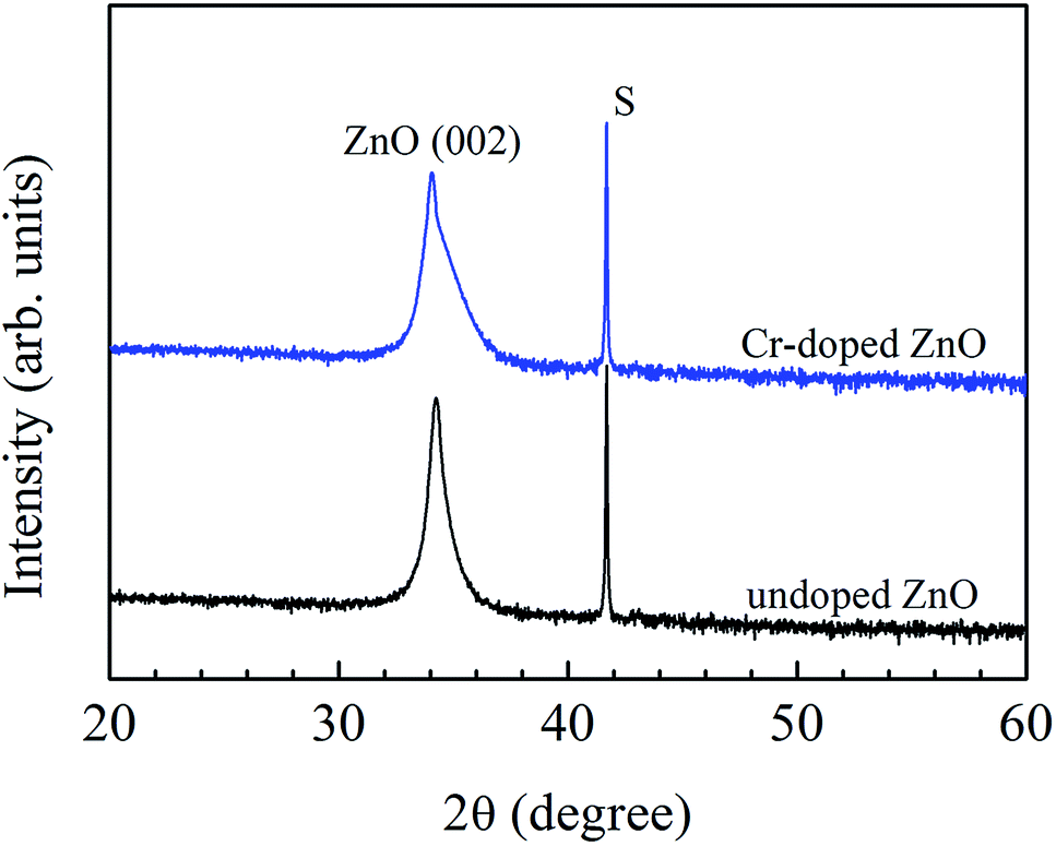 | ||
| Fig. 1 The θ–2θ scans of GIXRD of undoped and Cr-doped ZnO films. “S” indicates the peak originating from the c-sapphire substrates. | ||
Fig. 2 presents the XPS spectra of the O 1s, Zn 2p, and Cr 2p states in the undoped and Cr-doped ZnO films. In Fig. 2(a), the Gaussian fitting results of O 1s state illustrate that the asymmetric peak in both ZnO-based films contains three peaks at 529.8 eV, 531 eV, and 532.4 eV. The binding energy (BE) value of the peak at 529.8 eV can be allocated to O2− ions in the crystal structures encircled with Zn ions,33,34 and the peak at 532.4 eV was assigned to the loosely bound O ions on the thin films surface, such as adsorption H2O and O2.35,36 Moreover, the BE value of the peak at 531 eV has been attributed to the rich VO in the films.37,38 It is worth noting that for the Cr-doped ZnO film, noticeable reductions in both the peak intensity and the integrated area of the XPS signal occur at 529.8 eV, and increases in both the energy peak and integrated area of the XPS signal occur at 531 eV (as indicated in pink color in Fig. 2(a)). In Fig. 2(b), the peak value of Zn 2p3/2 and Zn 2p1/2 states for the undoped ZnO film were found at 1021.6 eV and 1044.7 eV, respectively, which can be ascribed to Zn ions bound to O ions. This BE value of the ZnO films are smaller than that of bulk value (1022.2 and 1045 eV),39 which indicates that the films are oxygen deficiency.40 In fact, the BE value of the Zn 2p state in Cr-doped ZnO film is smaller than that in the undoped ZnO film, clearly indicating considerable oxygen deficiency in the Cr-doped ZnO film. The deficiency of O2− bonding with Zn2+ may be due to the plenty of VO in the Cr-doped ZnO films as a result of the Cr dopant. For the Cr-doped ZnO thin films, the Cr 2p3/2 and 2p1/2 states were observed at 575.6 eV and 585.6 eV, respectively, which correspond to Cr2+ ions, as shown in Fig. 2(c). Clearly, a few Cr2+ have been substituted for Zn2+ sites, as shown by the detection of the Cr2+ signal from the Cr-doped ZnO film. Notice that the BE values of the Cr 2p3/2 and Cr 2p1/2 states are smaller than that of bulk values (576 eV and 586.9 eV),41,42 as depicted by a dotted line, which confirms the substantial oxygen deficiency in the Cr-doped ZnO film.
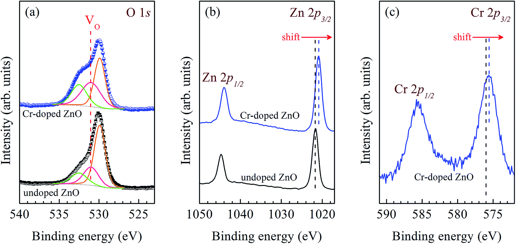 | ||
| Fig. 2 (a) O 1s, (b) Zn 2p, and (c) Cr 2p states XPS spectra of undoped and Cr-doped ZnO films. | ||
The schematic showing the Pt/ZnO-based/IZO multilayer structure was illustrated in inset of Fig. 3(a). Fig. 3(a) and (b) presents the current–voltage (I–V) curves recorded in the direct current sweeping mode. The sequence of bias voltages has been operated in the order of 0 V → 2.5 V → −2 V → 0 V. In order to conserve the sample from everlasting disruption, the compliance current was maintained at 1 mA. The bipolar RS behavior could be observed in both undoped and Cr-doped ZnO thin films. No forming process has been found in all the samples, which is a sign of the plenty of VO pre-existing in the as-deposited thin films. This phenomenon indicates that the VO can help to the fast formation of CFs, which leads to RS effect in the ZnO-based thin films. The set voltages for the undoped and Cr-doped ZnO thin films were found to be 1.87 V and 0.89 V, respectively. The reset voltages for the undoped and Cr-doped ZnO thin films were found to be −1.62 V and −0.86 V, respectively. Clearly, the set voltage for Cr-doped ZnO thin film were smaller than those for undoped ZnO thin film due to the existence of abundant VO in Cr-doped ZnO thin films, which helped to initiate the set process with relative ease. Additionally, the on/off current ratios for undoped and Cr-doped ZnO thin films were respectively found to be 3.51 × 101 and 9.12 × 10². In order to verify the reliability and stability of all the samples, endurance and retention times have been examined for the undoped and Cr-doped ZnO thin films, as displayed in Fig. 3(c)–(f). As can be seen in the figures, all of the ZnO-based thin films can be operated between low-resistance states (LRS) and high-resistance states (HRS) over 105 cycles. Moreover, the current value of all the ZnO-based thin films did not show obvious change when switched between LRS and HRS over a period of 105 seconds, thus demonstrating that the RS characteristic was extremely reliable and stable.
 | ||
| Fig. 3 Typical I–V curves of (a) ZnO and (b) Cr-doped ZnO thin films. The inset of (a) displays schematic diagram of the Pt/ZnO/IZO structures. Endurance examination of (c) ZnO and (d) Cr-doped ZnO. Retention time tests of (e) ZnO and (f) Cr-doped ZnO. | ||
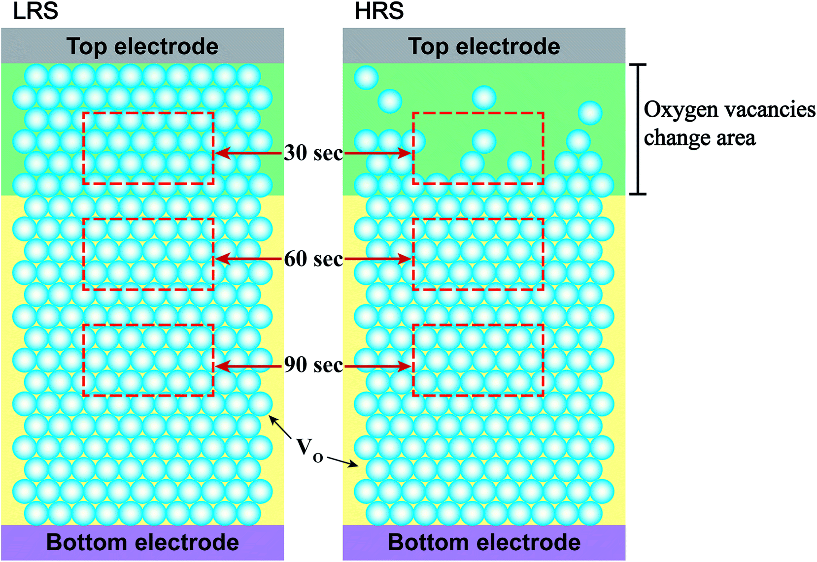
To study the chemical properties further, the depth-profiling XPS analysis was performed at different depths of the thin films. Fig. 4(a) and (b) shows the O 1s state XPS spectra of Cr-doped ZnO films at LRS and HRS, respectively, after sputtering etching for 30, 60, and 90 s. The two compositions, including O2− (529.8 eV) and VO (531 eV), are exist in the Cr-doped ZnO films. There was no noticeable change in the peak position of all the peaks after sputtering etching. The ratios of the O2− and VO components estimated from the integration areas of the O 1s XPS peaks at different depths of the thin films were displays in Fig. 4(c) and (d). No the integral area of the peak indicated any obvious change for all of the signals after sputtering etching in the Cr-doped ZnO films at LRS. In contrast, the integrated area of the VO peak at HRS increased with increasing sputtering etching time. It suggests that this phenomenon may be attributed to CFs mechanism, as shown in Fig. 5. During the set process, the VO were evenly arrayed between the top and bottom electrodes in the thin films, thereby leading to LRS. After the reset process, the VO-CFs have been destroyed near the top electrode when resistance state switches to HRS. Therefore, for the O 1s XPS spectra of the depth-profiling analysis at HRS, the VO evidently decreased in the thin film after sputtering etching for 30 seconds. On the other hand, as aforementioned, the RS effect could also be related to an interface-type mechanism, a phenomenon that takes place near the electrode/insulator interface, as displayed in Fig. 6. To summarize, both the CFs model and interface-type mechanism can be attributed to changes in VO.
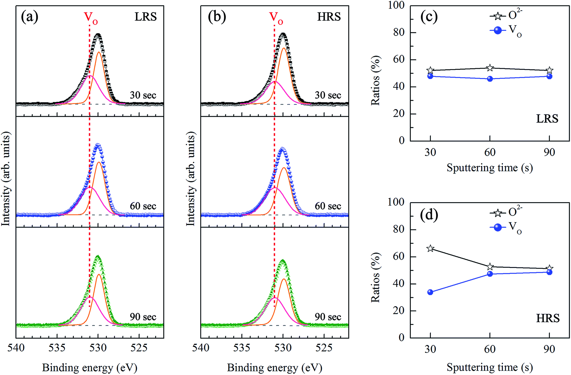 | ||
| Fig. 4 O 1s XPS spectra of Cr-doped ZnO thin films at (a) LRS and (b) HRS after various sputtering etching times. Ratios of the O2− and VO components in (c) LRS and (d) HRS at different depths. | ||
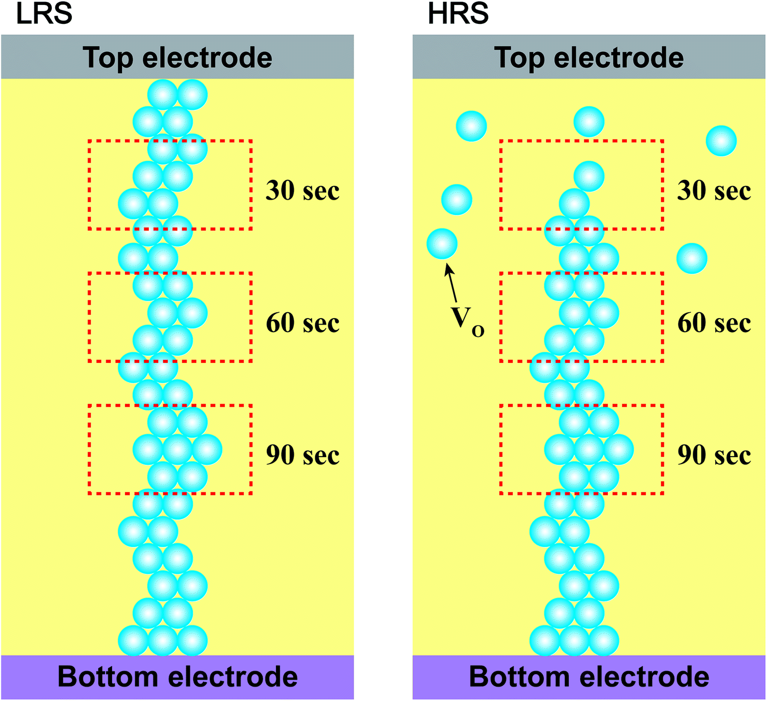 | ||
| Fig. 5 Schematic configuration of the RS mechanisms at LRS and HRS. The sputtering etching times are indicated by the red rectangle dotted line. | ||
 | ||
| Fig. 6 The interface-type mechanisms of the RS effect at LRS and HRS. | ||
As mentioned previously, the bipolar RS behavior observed for the ZnO thin film is possibly derived from the presence of VO in the films. From the XPS spectra, the VO was observed in all the films. Both the VO peak intensity and the integrated area of the Cr-doped ZnO film is larger than that of the undoped ZnO film, which is a strong indication of an increase in the VO concentration in the Cr-doped ZnO film. The increase of VO concentration due to Cr dopant, and it can be attributed to the Cr2+ ion radii (0.73 pm) was different from Zn2+ ion radii (0.74 pm), leading to more defects in the Cr-doped ZnO film. As the depth-profiling analysis of XPS spectra, the RS effect could be attributed to CFs and interface-type mechanism. Additionally, the set voltage and LRS/HRS ratio of Cr-doped ZnO was smallest and largest, respectively, exhibiting a notably high performance. In our study, the high VO concentration enhanced device performance of Cr-doped ZnO RS memory is achieved by using Cr dopant.
Conclusions
In summary, the effect of Cr doping on the defects-enhanced bipolar RS behavior in ZnO-based thin films was investigated. The RS effect was intimately related to the defect concentration in the films. Interestingly, the Cr doping changes the VO concentration, and the increase in the VO finally leads to an improvement of device performance for the Cr-doped ZnO film. Especially, the depth-profiling analysis of XPS spectra demonstrated that the RS effect could be corresponded to variations in the concentration of the defects. Our device not only possesses stable RS behavior but can also endure the great number of on/off RS cycles over a period exceeding one day without significant degradation in electrical characteristics. Notably, the bipolar RS characteristics obtained here exhibits excellent stability and reproducibility. The results evidently indicate that defect concentration is a key factor controlling the RS behavior in ZnO-based thin films, which are expected to be applicable to next-generation memory devices.Conflicts of interest
There are no conflicts to declare.Acknowledgements
This study was financially supported by the Ministry of Science and Technology of Taiwan (Grant No. MOST-104-2221-E-006-001, MOST-104-2221-E-168-011-MY3, and MOST-107-2221-E-006-185-MY3), and the authors would also like to thank the Ministry of Education of Taiwan, R. O. C. for the financial support under contract No. 107-N-270-EDU-T-142.References
- C. Chappert, A. Fert and F. N. Van Dau, Nat. Mater., 2007, 6, 813 CrossRef CAS PubMed.
- R. Waser and M. Aono, Nat. Mater., 2007, 6, 833 CrossRef CAS PubMed.
- A. Sawa, Mater. Today, 2008, 11, 28–36 CrossRef CAS.
- F. Pan, S. Gao, C. Chen, C. Song and F. Zeng, Mater. Sci. Eng., R, 2014, 83, 1–59 CrossRef.
- A. Makarov, V. Sverdlov and S. Selberherr, Microelectron. Reliab., 2012, 52, 628–634 CrossRef.
- J. J. Yang, M. D. Pickett, X. Li, D. A. A. Ohlberg, D. R. Stewart and R. S. Williams, Nat. Nanotechnol., 2008, 3, 429 CrossRef CAS PubMed.
- Z. Q. Wang, H. Y. Xu, L. Zhang, X. H. Li, J. G. Ma, X. T. Zhang and Y. C. Liu, Nanoscale, 2013, 5, 4490–4494 RSC.
- F. M. Simanjuntak, D. Panda, T.-L. Tsai, C.-A. Lin, K.-H. Wei and T.-Y. Tseng, Appl. Phys. Lett., 2015, 107, 033505 CrossRef.
- Z. Fei, P. Shanshan, H. Congli, Z. Xiaojian, C. Xinxin, L. Yiwei and L. Run-Wei, Nanotechnology, 2011, 22, 275204 CrossRef PubMed.
- Y. Lai, P. Xin, S. Cheng, J. Yu and Q. Zheng, Appl. Phys. Lett., 2015, 106, 031603 CrossRef.
- B. Wang, T. Ren, S. Chen, B. Zhang, R. Zhang, J. Qi, S. Chu, J. Huang and J. Liu, J. Mater. Chem. C, 2015, 3, 11881–11885 RSC.
- C.-W. Huang, J.-Y. Chen, C.-H. Chiu and W.-W. Wu, Nano Lett., 2014, 14, 2759–2763 CrossRef CAS PubMed.
- J. Qi, M. Olmedo, J. Ren, N. Zhan, J. Zhao, J.-G. Zheng and J. Liu, ACS Nano, 2012, 6, 1051–1058 CrossRef CAS PubMed.
- G. Chen, C. Song, C. Chen, S. Gao, F. Zeng and F. Pan, Adv. Mater., 2012, 24, 3515–3520 CrossRef CAS PubMed.
- T.-H. Huang, P.-K. Yang, W.-Y. Chang, J.-F. Chien, C.-F. Kang, M.-J. Chen and J.-H. He, J. Mater. Chem. C, 2013, 1, 7593–7597 RSC.
- J. F. Gibbons and W. E. Beadle, Solid-State Electron., 1964, 7, 785–790 CrossRef CAS.
- X.-J. Zhu, J. Shang and R.-W. Li, Front. Mater. Sci., 2012, 6, 183–206 CrossRef.
- R. Waser, R. Dittmann, G. Staikov and K. Szot, Adv. Mater., 2009, 21, 2632–2663 CrossRef CAS.
- R. Muenstermann, T. Menke, R. Dittmann and R. Waser, Adv. Mater., 2010, 22, 4819–4822 CrossRef CAS PubMed.
- S. Bagdzevicius, K. Maas, M. Boudard and M. Burriel, J. Electroceram., 2017, 39, 157–184 CrossRef CAS.
- C.-H. Huang, J.-S. Huang, C.-C. Lai, H.-W. Huang, S.-J. Lin and Y.-L. Chueh, ACS Appl. Mater. Interfaces, 2013, 5, 6017–6023 CrossRef CAS PubMed.
- Y. Vadim Sh, U. Y. Shavkat, K. Yeon Soo and P. Bae Ho, Nanotechnology, 2012, 23, 375201 CrossRef PubMed.
- A. Janotti and C. G. Van de Walle, Phys. Rev. B: Condens. Matter Mater. Phys., 2007, 76, 165202 CrossRef.
- M. Janousch, G. I. Meijer, U. Staub, B. Delley, S. F. Karg and B. P. Andreasson, Adv. Mater., 2007, 19, 2232–2235 CrossRef CAS.
- M. Lanza, H.-S. P. Wong, E. Pop, D. Ielmini, D. Strukov, B. C. Regan, L. Larcher, M. A. Villena, J. J. Yang, L. Goux, A. Belmonte, Y. Yang, F. M. Puglisi, J. Kang, B. Magyari-Köpe, E. Yalon, A. Kenyon, M. Buckwell, A. Mehonic, A. Shluger, H. Li, T.-H. Hou, B. Hudec, D. Akinwande, R. Ge, S. Ambrogio, J. B. Roldan, E. Miranda, J. Suñe, K. L. Pey, X. Wu, N. Raghavan, E. Wu, W. D. Lu, G. Navarro, W. Zhang, H. Wu, R. Li, A. Holleitner, U. Wurstbauer, M. C. Lemme, M. Liu, S. Long, Q. Liu, H. Lv, A. Padovani, P. Pavan, I. Valov, X. Jing, T. Han, K. Zhu, S. Chen, F. Hui and Y. Shi, Adv. Electron. Mater., 2018, 1800143 Search PubMed.
- B. Govoreanu, G. S. Kar, Y. Chen, V. Paraschiv, S. Kubicek, A. Fantini, I. P. Radu, L. Goux, S. Clima, R. Degraeve, N. Jossart, O. Richard, T. Vandeweyer, K. Seo, P. Hendrickx, G. Pourtois, H. Bender, L. Altimime, D. J. Wouters, J. A. Kittl and M. Jurczak, 2011 International Electron Devices Meeting, 2011, pp. 31.6.1–31.6.4 Search PubMed.
- F. M. Simanjuntak, D. Panda, K.-H. Wei and T.-Y. Tseng, Nanoscale Res. Lett., 2016, 11, 368 CrossRef PubMed.
- H. Xu, D. H. Kim, Z. Xiahou, Y. Li, M. Zhu, B. Lee and C. Liu, J. Alloys Compd., 2016, 658, 806–812 CrossRef CAS.
- A. Younis, D. Chu and S. Li, Nanoscale Res. Lett., 2013, 8, 154 CrossRef PubMed.
- D. L. Xu, Y. Xiong, M. H. Tang, B. W. Zeng, J. Q. Li, L. Liu, L. Q. Li, S. A. Yan and Z. H. Tang, Microelectron. Eng., 2014, 116, 22–25 CrossRef CAS.
- Y. M. Hu, S. S. Li and C. H. Chia, Appl. Phys. Lett., 2011, 98, 052503 CrossRef.
- Y. M. Hu, C. W. Hsu, C. Y. Wang, S. S. Lee, J. W. Chiou, T. C. Han, G. J. Chen, W. Y. Chou and J. Chang, Thin Solid Films, 2010, 518, 2916–2919 CrossRef CAS.
- E. De la Rosa, S. Sepúlveda-Guzman, B. Reeja-Jayan, A. Torres, P. Salas, N. Elizondo and M. J. Yacaman, J. Phys. Chem. C, 2007, 111, 8489–8495 CrossRef CAS.
- Q. Gao, Y. Dai, C. Li, L. Yang, X. Li and C. Cui, J. Alloys Compd., 2016, 684, 669–676 CrossRef CAS.
- M. Jongsun, H. Sungho, J. Gunho, C. Minhyeok, K. Seonghyun, H. Hyunsang and L. Takhee, Nanotechnology, 2009, 20, 095203 CrossRef PubMed.
- X. Li, Y. Wang, W. Liu, G. Jiang and C. Zhu, Mater. Lett., 2012, 85, 25–28 CrossRef CAS.
- M. Chen, X. Wang, Y. H. Yu, Z. L. Pei, X. D. Bai, C. Sun, R. F. Huang and L. S. Wen, Appl. Surf. Sci., 2000, 158, 134–140 CrossRef CAS.
- S. Baek, J. Song and S. Lim, Phys. B, 2007, 399, 101–104 CrossRef CAS.
- S. X. Ren, G. W. Sun, J. Zhao, J. Y. Dong, Y. Wei, Z. C. Ma, X. Zhao and W. Chen, Appl. Phys. Lett., 2014, 104, 232406 CrossRef.
- Y. D. Chiang, W. Y. Chang, C. Y. Ho, C. Y. Chen, C. H. Ho, S. J. Lin, T. B. Wu and J. H. He, IEEE Trans. Electron Devices, 2011, 58, 1735–1740 CAS.
- C. Xu, M. Hassel, H. Kuhlenbeck and H. J. Freund, Surf. Sci., 1991, 258, 23–34 CrossRef CAS.
- E. Desimoni, C. Malitesta, P. G. Zambonin and J. C. Rivière, Surf. Interface Anal., 1988, 13, 173–179 CrossRef CAS.
| This journal is © The Royal Society of Chemistry 2019 |