
 Open Access Article
 This Open Access Article is licensed under a Creative Commons Attribution-Non Commercial 3.0 Unported Licence
Exploring the temperature effect on hole transport properties in organic bulk heterojunctions
Bixin Li *,
Shiyang Zhang and
Xianglin Li
*,
Shiyang Zhang and
Xianglin Li
Department of Science Education, Laboratory of College Physics, Hunan First Normal University, Changsha 410205, People's Republic of China. E-mail: lbxin86@hotmail.com
First published on 23rd January 2019
Abstract
The temperature effect on hole transport in representative organic bulk heterojunctions has been explored. Two model systems, namely, copper phthalocyanine (CuPc):fullerene (C60), and zinc phthalocyanine (ZnPc):C60, are chosen as case studies. The current–voltage (I–V) characteristics have been measured in hole-only configurations in the temperature range of 100–280 K and the temperature-dependent hole transport process has been revealed. At high voltages and temperatures from 180 to 280 K, charge transport is governed by the trapping model with space charge limited conduction in the presence of an exponential trap distribution. However, at temperatures below 180 K, the mobility model with field-dependent mobility fits the experimental data well, indicating that charge conduction occurs through a hopping mechanism. The extended state and localized state affected by temperature are responsible for hole transport in high and low temperature ranges, respectively.
1. Introduction
The bulk heterojunction (BHJ) blend of an electron donor and an electron acceptor material is a promising candidate for next-generation organic solar cells (OSCs).1 In particular, metal phthalocyanine and fullerene (C60) are typical small molecule donor and acceptor materials, respectively. Despite the rapid progress in power conversion efficiency in OSCs, their performance and stability are still lower than those of their inorganic-based counterparts. A key factor which determines the device efficiency is the charge carrier transport property in bulk organic films.2,3 High carrier mobility materials will improve charge transport and reduce carrier recombination; hence the device efficiency will be enhanced. Therefore, understanding the basic charge transport behavior is of great importance to designing high-efficiency OSCs.Many studies of composition-dependent charge transport have been reported in polymer BHJs, such as poly(3-hexylthiophene) (P3HT):1-(3-methoxycarbonyl)-propyl-1-phenyl-(6,6)methanofullerene (PCBM),4–6 poly[2-methoxy-5-(3′,7′-dimethyloctyloxy)-1,4-phenylenevinylene] (MDMO-PPV):PCBM,7,8 and polyfluorene:PCBM.9 In these studies, charge transport was investigated by the time-of-flight (TOF) method, which generally requires several micron-thick films, rendering it difficult to replicate the morphology of the film used in a real device.10 Ambipolar charge carrier transport has also been studied in copper phthalocyanine (CuPc):C60 and other organic BHJs by the organic thin film transistor (OTFT) technique.11–14 However, charge carriers move in the direction parallel to thin films within a very thin insulator–organic interface region, which is different from those movements in OSCs. Notably, space charge limited current (SCLC) measurement, which requires thinner film thickness, is a powerful and convenient method to evaluate the charge transport process in pristine film or BHJs.15–19
The charge carrier transport process is always accompanied by the capture of some carriers in localized states, which might act as recombination centres or traps. Generally, there are two models to describe the transport mechanism, i.e.: (i) the trapping model, which assumes a certain distribution of traps in energy spaces and (ii) the mobility model, which assumes an electric field dependence of mobility.20,21 The effect of cadmium selenide (CdSe) quantum dots on hole transport in P3HT has been studied over a wide temperature range and the transport mechanism differs. A comparative study on CuPc:C60 and zinc phthalocyanine (ZnPc):C60 BHJs revealed trap-limited conduction above 180 K.19 Lou et al. investigated the charge transport and electronic traps in P3HT:PCBM BHJ based on current–voltage (I–V) measurement in the temperature range 213–293 K.15 Nevertheless, the study of carrier transport in organic BHJs under a wider temperature is still a matter of debate.
In this work, steady temperature-dependent I–V measurements were used to comprehensively investigate the hole transport properties in CuPc:C60 and ZnPc:C60 BHJs from 100 to 280 K. By analyzing the I–V curves, we observe that the charge transport mechanism shows a transition from the mobility model at low temperature to the trap model at high temperature for both organic BHJs. The origin of the difference caused by temperature is discussed in detail.
2. Experimental details
CuPc and ZnPc were purchased from Alfa Aesar and purified by temperature gradient sublimation. The hole-only devices were constructed in the sandwiched configuration of ITO/PEDOT:PSS (40 nm)/CuPc:C60 or ZnPc:C60 (1![[thin space (1/6-em)]](https://www.rsc.org/images/entities/char_2009.gif) :1, 120 nm)/MoO3 (5 nm)/Al, where ITO is indium-tin-oxide, PEDOT:PSS is poly(ethylene-dioxythiophene):polystyrenesulfonate (CLEVIOS P VP Al 4083, H. C. Stark), and MoO3 is molybdenum oxide. PEDOT:PSS and MoO3 were used to facilitate hole injection from ITO and suppress electron injection from Al.22,23 A 40 nm thick layer of PEDOT:PSS was spin coated onto precleaned and plasma-treated ITO coated glass substrates at 3000 rpm and cured at 120 °C for 30 min in a vacuum. After drying, the organic BHJs were deposited under a high vacuum (pressure < 10−4 Pa) by a coevaporation process. Al (∼100 nm) electrodes were deposited on the organic films through shadow masks. The deposition rates of the organic materials and Al electrode were controlled at 2 Å s−1 and 10 Å s−1, respectively. The active area of each device was 16 mm2.
:1, 120 nm)/MoO3 (5 nm)/Al, where ITO is indium-tin-oxide, PEDOT:PSS is poly(ethylene-dioxythiophene):polystyrenesulfonate (CLEVIOS P VP Al 4083, H. C. Stark), and MoO3 is molybdenum oxide. PEDOT:PSS and MoO3 were used to facilitate hole injection from ITO and suppress electron injection from Al.22,23 A 40 nm thick layer of PEDOT:PSS was spin coated onto precleaned and plasma-treated ITO coated glass substrates at 3000 rpm and cured at 120 °C for 30 min in a vacuum. After drying, the organic BHJs were deposited under a high vacuum (pressure < 10−4 Pa) by a coevaporation process. Al (∼100 nm) electrodes were deposited on the organic films through shadow masks. The deposition rates of the organic materials and Al electrode were controlled at 2 Å s−1 and 10 Å s−1, respectively. The active area of each device was 16 mm2.
The thickness was controlled in situ by a quarter crystal monitor, and calibrated by a Dektak 6M Profiler (Veeco). The I–V characteristics were carried out using a Keithley 2400 sourcemeter integrated with a vacuum cryostat (Optistat DN-V, Oxford Instruments) and an ITC 601 temperature controller in the temperature range 100–280 K. The devices were presented in a sample holder and liquid nitrogen was used as a cooling medium.
3. Results and discussion
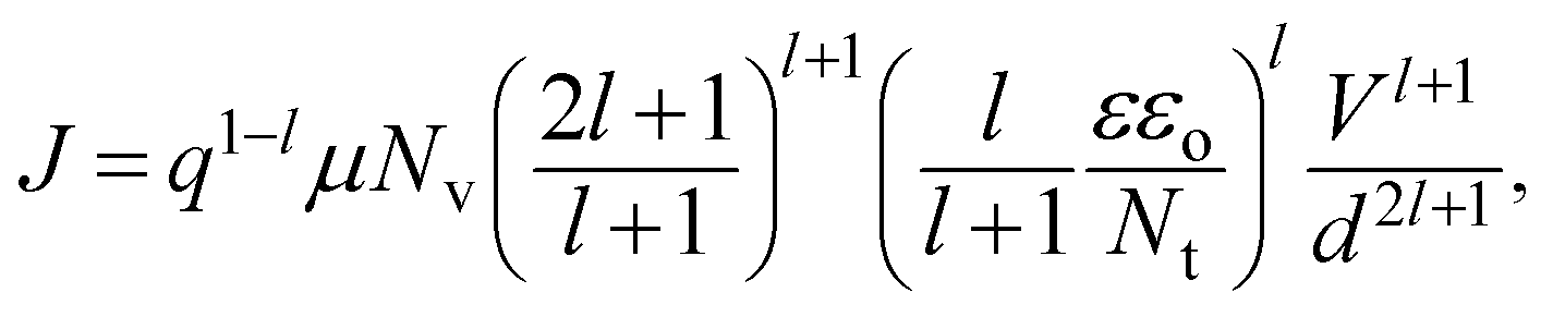
Fig. 1 presents the I–V characteristics of the hole-only devices for CuPc:C60 and ZnPc:C60 BHJs at various temperatures in a log–log scale. It is clearly observable that at relatively high bias voltages, the non-linear I–V curves follow the power law J ∝Vm with m > 2 at 280 K and that m increases with decreasing temperature. This feature may signify an SCLC current with an exponential distribution of traps in energy and space. Using continuous equation and boundary condition as| J = qμp(x)E(x), | (1) |
 | (2) |
 | (3) |
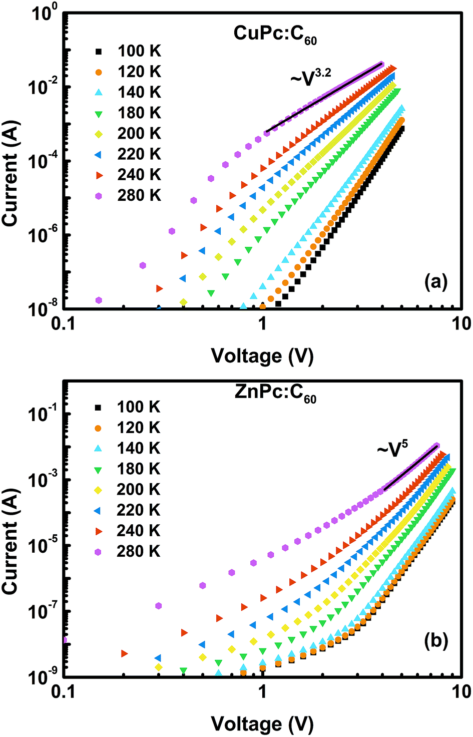 | ||
| Fig. 1 Current–voltage characteristics of the hole-only devices in the temperature range 100–280 K based on BHJ films of (a) CuPc:C60 and (b) ZnPc:C60. Solid lines are linear fits to trap model eqn (3). | ||
In particular, we note that the current density decreases with decreasing temperature. Furthermore, based on the feature of I dependence on V and T, two distinct regions have been identified. In the high-temperature region, 180–280 K, the curves tend to converge to a common point.25 However, this trend is indistinct under 140 K, the low-temperature region. These results may imply that the transport mechanism differs in the two regions.
Earlier studies have shown that in conducting polymers the charge limited conduction governs the transport either by the trap model at higher temperature or by the mobility model at lower temperature.26 In the mobility model, mobility obeys the empirical law21
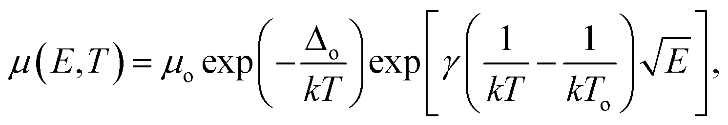 | (4) |
In order to elucidate the different underlying transport mechanisms, the activation energy was analyzed. Eqn (3) can be simplified to obtain the carrier density and activation energy of traps as25
 | (5) |
Eqn (5) provides the Arrhenius dependence of current density on temperature and gives the activation energy as
 | (6) |
The temperature dependences of the current at an applied voltage for the CuPc:C60 and ZnPc:C60 devices are shown in Fig. 2. The plot shows two distinct linear regions for both films, one at a high-temperature regime and the other at a low-temperature regime. The slope of the high-temperature regime is definitely larger than that of the low-temperature regime, which signifies that the activation energy is much larger in the high-temperature regime. These results further confirm that the conduction mechanism varies in the two regimes for both films.
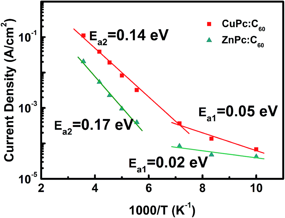 | ||
| Fig. 2 J vs. 1000/T plots for CuPc:C60 and ZnPc:C60 at 3 V and 6 V, respectively. Solid lines are fits to eqn (5). | ||
Consequently, I–V curves from 100 to 280 K for both films have been comprehensively analyzed by the trap model using eqn (3) and the mobility model using eqn (4), as shown in Fig. 3 and 4. We can clearly observe that the trap model and mobility model determine the I–V characteristics over different temperature ranges. In Fig. 3(a), the experimental data agrees well with the trap model rather than the mobility model, with the correlation coefficients r being 0.99985 and 0.99881, respectively. The fitting parameters obtained are μ = 1.0 × 10⁻⁵ cm2 V−1 s−1, Nv = 1.0 × 1019 cm−3, Nt = 2.7 × 1017 cm−3. However, the trap model shows great discrepancy with the experimental data from 100 to 140 K in Fig. 3(b). Dashed lines represent the theoretically generated curves using the mobility model at different temperatures and they agree well with the experimental data, with the parameters being μo = 4.5 × 10⁻⁹ cm2 V−1 s−1, and γ = 7.0 × 10⁻⁵ eV cm−1/2 V−1/2. In addition, by extrapolating the activation energy at different voltages to zero field, as presented in Fig. 5, the zero field activation energy Δo is found to be 0.096 eV.
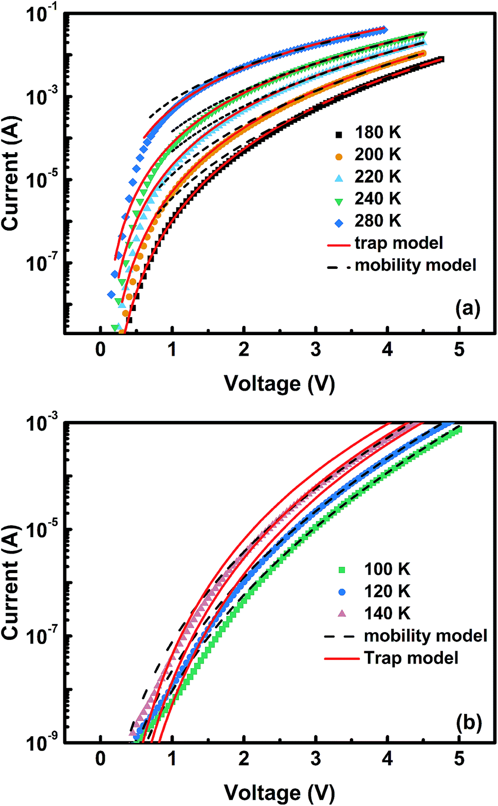 | ||
| Fig. 3 Current–voltage characteristics of CuPc:C60 hole-only devices in (a) the higher temperature range and (b) the lower temperature range. Solid lines and dashed lines are fits to eqn (3) and (4), respectively. | ||
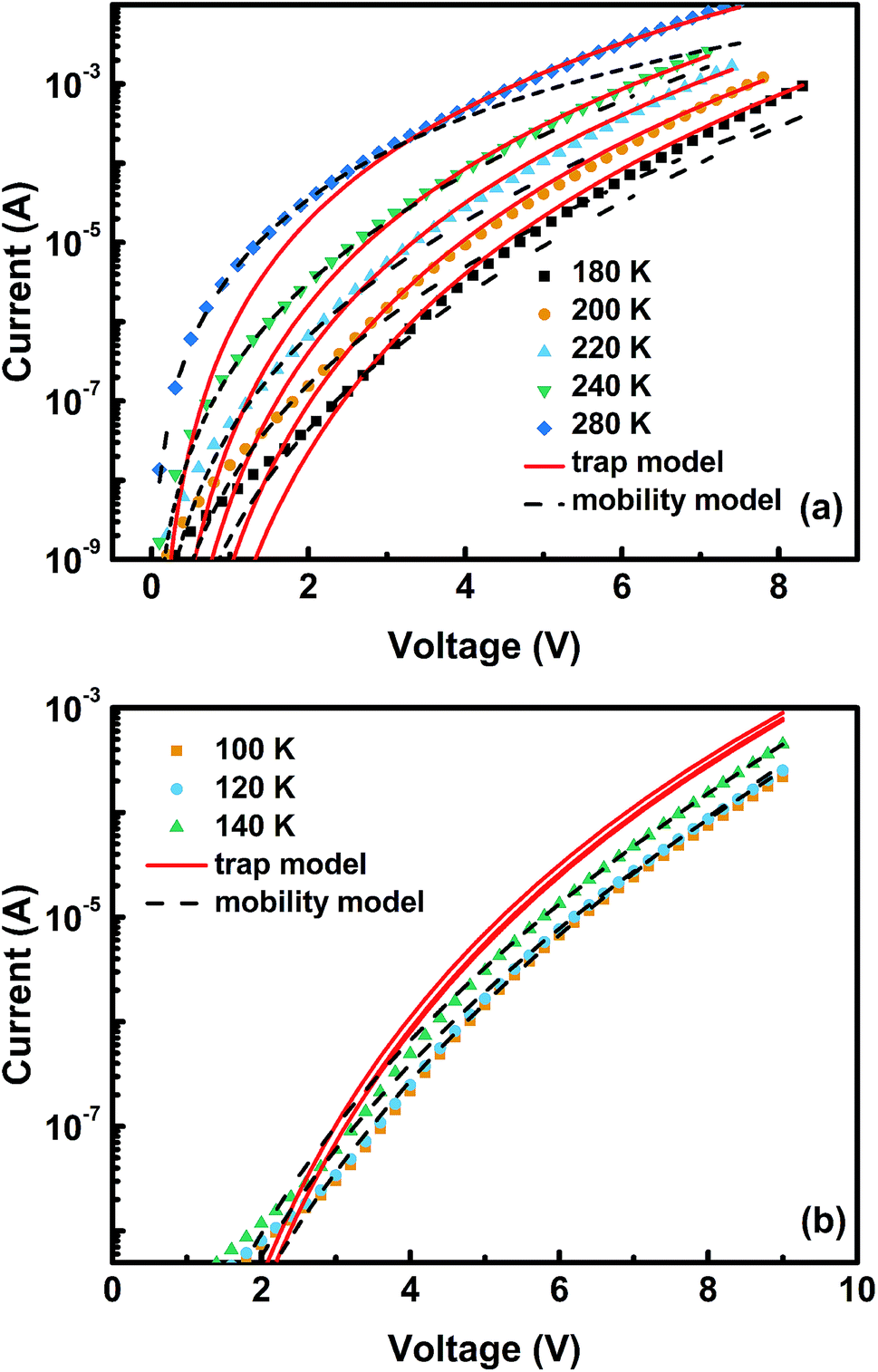 | ||
| Fig. 4 Current–voltage characteristics of ZnPc:C60 hole-only devices in (a) the higher temperature range and (b) the lower temperature range. Solid lines and dashed lines are fits to eqn (3) and (4), respectively. | ||
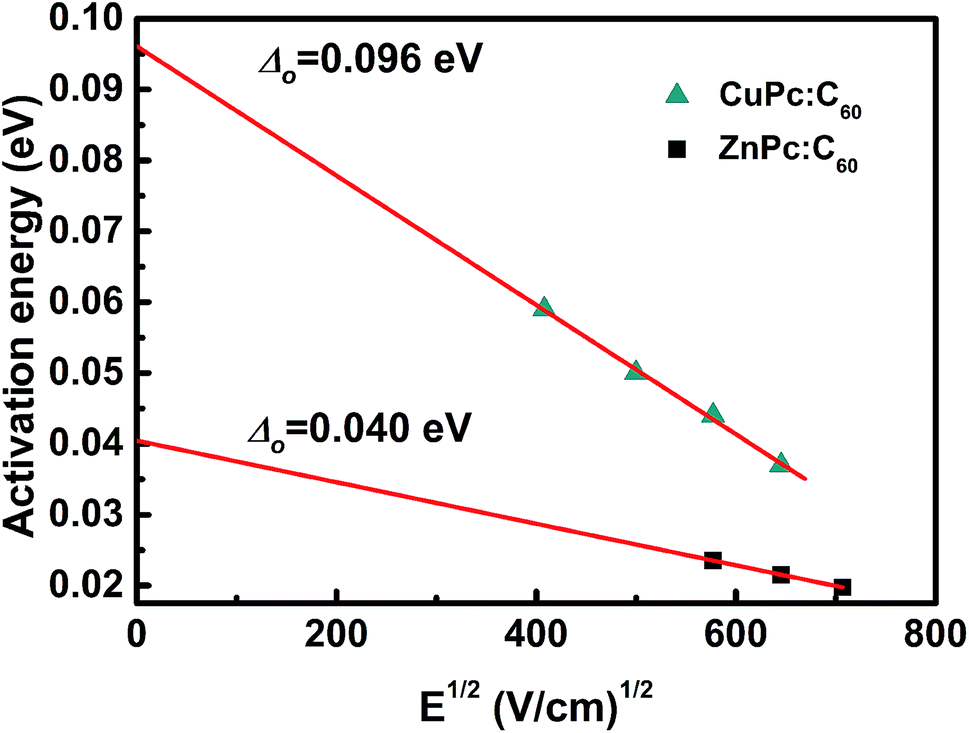 | ||
| Fig. 5 Low-temperature activation energy versus the square root of the electric field. Solid lines are extrapolations to zero field. | ||
As demonstrated by Fig. 4, a similar phenomenon can also be noted for the ZnPc:C60 BHJ film. From 180 to 280 K, the entire set of data fits better with the trap model (r = 0.99882) than the mobility model (r = 0.99694). The values of the fitting parameters in this case are μ = 6.2 × 10⁻⁶ cm2 V−1 s−1, Nv = 1.0 × 1019 cm−3, and Nt = 5.0 × 1017 cm−3. These values are then used to predict the currents at lower temperatures. In contrast, the predicted results clearly overestimate the experimental data over a wide voltage range, while the mobility model shows excellent agreement from 100 K to 140 K. The parameters obtained are μo = 8.23 × 10⁻¹³ cm2 V−1 s−1, γ = 5.4 × 10⁻⁵ eV cm−1/2 V−1/2 and Δo = 0.040 eV.
Hence, the temperature is responsible for the different transport mechanisms in BHJs.26 It is well known that there are extended states and localized states in the material. Both extended and localized states should play an important role in the transport process in the same way as in inorganic amorphous materials.27 In the high-temperature region, a sufficient number of holes are ionized from localized states to extended states. The current is mainly through the drift of carriers in the extended states with periodic trapping–detrapping in the localized states.28 Therefore, the trap model prevails. However, at lower temperatures, the carriers in the localized states gain inadequate energy to be excited to the extended states. Thus the conduction takes place through the hopping of carriers from one localized state to another, which shows field and temperature dependence. As a result, the mobility model is justified in the low-temperature region.
4. Conclusions
In conclusion, it is demonstrated that temperature plays a significant role in controlling the hole transport process in CuPc:C60 and ZnPc:C60 BHJ films. At high temperatures the conduction can be illustrated by the trap model with carriers moving through the extended states. Whereas at low temperatures, the transport is governed by the mobility model with carriers hopping through the localized states. This work assists in gaining a fundamental understanding of the electrical properties of organic BHJ films that govern device behavior and provides guidance for further device optimization.Conflicts of interest
There are no conflicts of interest to declare.Acknowledgements
The authors gratefully acknowledge the Hunan First Normal University Research Fund (XYS15N01), the Scientific Research Fund of Hunan Provincial Education Department (17C0331), and the Natural Science Foundation of Hunan Province (Grant No. 2017JJ3046) for their support of this research.References
- D. Meissner and J. Rostalski, Synth. Met., 2001, 121, 1551–1552 CrossRef CAS
.
- G. Dennler, M. C. Scharber and C. J. Brabec, Adv. Mater., 2009, 21, 1 CrossRef
- H. Yin, P. Bi, S. H. Cheung, W. L. Cheng, K. L. Chiu, C. H. Y. Ho, H. W. Li, S. W. Tsang, X. Hao and S. K. So, Sol. RRL, 2018, 2, 1700239 CrossRef
- V. Chellappan, G. M. Ng, M. J. Tan, W.-P. Goh and F. Zhu, Appl. Phys. Lett., 2009, 95, 263305 CrossRef
- A. Baumann, J. Lorrmann, C. Deibel and V. Dyakonov, Appl. Phys. Lett., 2008, 93, 252104 CrossRef
- E. von Hauff, J. Parisi and V. Dyakonov, J. Appl. Phys., 2006, 100, 043702 CrossRef
- S. M. Tuladhar, D. Poplavskyy, S. A. Choulis, J. R. Durrant, D. D. C. Bradley and J. Nelson, Adv. Funct. Mater., 2005, 15, 1171–1182 CrossRef CAS
- S. A. Choulis, J. Nelson, Y. Kim, D. Poplavskyy, T. Kreouzis, J. R. Durrant and D. D. C. Bradley, Appl. Phys. Lett., 2003, 83, 3812 CrossRef CAS
- R. Pacios, J. Nelson, D. D. C. Bradley and C. J. Brabec, Appl. Phys. Lett., 2003, 83, 4764 CrossRef CAS
- P. M. Borsenberger and D. S. Weiss, Organic Photoreceptors for Imaging Systems, Dekker, New York, 1993 Search PubMed
- A. Opitz, M. Bronner and W. Brütting, J. Appl. Phys., 2007, 101, 063709 CrossRef
- M. Bronner, A. Opitz and W. Brütting, Phys. Status Solidi A, 2008, 205, 549–563 CrossRef CAS
- A. Opitz, J. Wagner, W. Brütting, A. Hinderhofer and F. Schreiber, Phys. Status Solidi A, 2009, 206, 2683–2694 CrossRef CAS
- A. Ko Ko Kyaw, D. Hwan Wang, H.-R. Tseng, J. Zhang, G. C. Bazan and A. J. Heeger, Appl. Phys. Lett., 2013, 102, 163308 CrossRef
- Y.-H. Lou, L. Zhang, M.-F. Xu, Z.-K. Wang, S. Naka, H. Okada and L.-S. Liao, Org. Electron., 2014, 15, 299–305 CrossRef CAS
- W. Yan-Ping, H. Jin-Ying, C. Jiang-Shan, Q. Xian-Feng, Y. De-Zhi, M. Dong-Ge and D. Li-Song, Chin. Phys. Lett., 2016, 33, 027302 CrossRef
- A. S. Sarkar and S. K. Pal, J. Phys. D: Appl. Phys., 2015, 48, 445501 CrossRef
- M. R. Khan, P. Anjaneyulu, K. S. R. Koteswara Rao and R. Menon, J. Phys. D: Appl. Phys., 2017, 50, 095103 CrossRef
- B. Li, J. Chen, D. Yang and D. Ma, Semicond. Sci. Technol., 2011, 26, 115006 CrossRef
- K. C. Kao and W. Huang, Electrical Transport in Solids, Pergamon, Oxford, 1981 Search PubMed
- W. D. Gill, J. Appl. Phys., 1972, 43, 5033–5040 CrossRef
- A. Opitz, M. Bronner, J. Wagner, M. Götzenbrugger and W. Brütting, Proc. SPIE, 2008, 7002, 70020J CrossRef
- M. Hoping, C. Schildknecht, H. Gargouri, T. Riedl, M. Tilgner, H. H. Johannes and W. Kowalsky, Appl. Phys. Lett., 2008, 92, 213306 CrossRef
- M. A. Lampert and P. Mark, Current Injection in Solids, Academic, New York, 1970 Search PubMed
- V. Kumar, S. C. Jain, A. K. Kapoor, J. Poortmans and R. Mertens, J. Appl. Phys., 2003, 94, 1283–1285 CrossRef CAS
- A. K. Kapoor, S. C. Jain, J. Poortmans, V. Kumar and R. Mertens, J. Appl. Phys., 2002, 92, 3835–3838 CrossRef CAS
- P. G. Le Comber and W. E. Spear, Phys. Rev. Lett., 1970, 25, 509–511 CrossRef CAS
- C. Li, L. Duan, H. Li and Y. Qiu, J. Phys. Chem. C, 2014, 118, 10651–10660 CrossRef CAS
| This journal is © The Royal Society of Chemistry 2019 |