
 Open Access Article
 This Open Access Article is licensed under a Creative Commons Attribution-Non Commercial 3.0 Unported Licence
Intense-pulsed-UV-converted perhydropolysilazane gate dielectrics for organic field-effect transistors and logic gates†
Han Sol Backac,
Min Je Kimb,
Jeong Ju Baeka,
Do Hwan Kim d,
Gyojic Shin*a,
Kyung Ho Choi*a and
Jeong Ho Cho*e
d,
Gyojic Shin*a,
Kyung Ho Choi*a and
Jeong Ho Cho*e
aResearch Institute of Sustainable Manufacturing System, Intelligent Sustainable Materials R&D Group, Korea Institute of Industrial Technology, Cheonan-si 331-822, Chungcheongnam-do, Republic of Korea. E-mail: gyshin@kitech.re.kr; khchoi@kitech.re.kr
bSKKU Advanced Institute of Nanotechnology (SAINT), Suwon 440-746, Republic of Korea
cSchool of Chemical Engineering, Sungkyunkwan University, Suwon 440-746, Republic of Korea
dDepartment of Chemical Engineering, Hanyang University, Seoul 04763, Republic of Korea
eDepartment of Chemical and Biomolecular Engineering, Yonsei University, Seoul 03722, Republic of Korea. E-mail: jhcho94@yonsei.ac.kr
First published on 23rd January 2019
Abstract
We fabricated a high-quality perhydropolysilazane (PHPS)-derived SiO2 film by intense pulsed UV irradiation and applied it as a gate dielectric layer in high-performance organic field-effect transistors (OFETs) and complementary inverters. The conversion process of PHPS to SiO2 was optimized by varying the number of intense pulses and applied voltage. The chemical structure and gate dielectric properties of the PHPS-derived SiO2 films were systematically investigated via Fourier transform infrared spectroscopy and leakage current measurements, respectively. The resulting PHPS-derived SiO2 gate dielectric layer showed a dielectric constant of 3.8 at 1 MHz and a leakage current density of 9.7 × 10⁻¹² A cm−2 at 4.0 MV cm−1. The PHPS-derived SiO2 film was utilized as a gate dielectric for fabricating benchmark p- and n-channel OFETs based on pentacene and N,N′-dioctyl-3,4,9,10-perylenedicarboximide (PTCDI-C8), respectively. The resulting OFETs exhibited good electrical properties, such as carrier mobilities of 0.16 (±0.01) cm2 V−1 s−1 (for the pentacene OFET) and 0.02 (±0.01) cm2 V−1 s−1 (for the PTCDI-C8 OFET) and an on–off current ratio larger than 105. The fabrication of the PHPS-derived SiO2 gate dielectric layer by a simple solution process and intense pulsed UV irradiation at room temperature serves as a novel approach for the realization of large-area flexible electronics in the flexible device industry of the future.
Introduction
Organic electronic devices such as organic light-emitting diodes,1 organic solar cells,2 and organic field-effect transistors (OFETs)3,4 have attracted significant attention because they offer several advantages such as large-area processability, low weight, ease of fabrication processability, and flexibility. In particular, an OFET is a fundamental component in the development of electronic devices such as displays,5 smart cards, and radio-frequency identification tags.6,7 In the past decade, the electrical properties of OFETs have been improved considerably and have already reached a level comparable to or even higher than the performance levels of amorphous Si transistors.4,8–10 In addition to the development of semiconductors with high carrier mobilities and electrodes with high conductivities, the development of gate dielectric materials is crucial for the fabrication of high-performance OFET devices. Thus far, high-performance OFETs have been achieved using inorganic gate dielectrics such as SiO2, Al2O3, and HfO2.11–13 However, they are usually prepared by complex, expensive vacuum processes such as physical vapor deposition,14,15 chemical vapor deposition,16,17 and atomic layer deposition.18,19SiO2 is one of the most important insulating materials for application as a gate dielectric or encapsulation layer in various electronic devices. Several research groups have fabricated the SiO2 layer by conversion of spin-on-glass (SOG) materials such as perhydropolysilazane (PHPS), silsesquioxane, tetraethyl orthosilicate, and tetramethyl orthosilicate.20–24 Because of the low cost, simplicity, and excellent substrate adaptability of this approach, this process can replace the conventional vapor deposition process. PHPS, used in this study, is one of the most widely used SOG materials because of its low carbon contamination and ability to form dense films.25–28 Among the various methods for the conversion of PHPS to SiO2, a commonly utilized one is thermal annealing.27,29 However, this process requires high temperatures above 500 °C, which limits the applicability of PHPS on polymer substrates with low glass transition temperatures. To overcome this problem, various types of low-temperature conversion methods using catalysts have been developed. For instance, gaseous ammonia30 or hydrogen peroxide31,32 can promote the conversion of PHPS to SiO2.32 However, achieving complete conversion of PHPS to SiO2 remains difficult. Furthermore, significant contamination by catalysts may result in a fatal defect in the film and degradation of the gate dielectric properties.
In this study, conversion of PHPS was performed using intense pulsed UV light (IPL), which is a rapid and efficient conversion method at room temperature. The conversion of PHPS to SiO2 by IPL irradiation is a more effective approach for the synthesis of a dense silica film than the previous method of using vacuum UV, which requires complicated equipment such as a vacuum chamber.33,34 Moreover, the former approach is more efficient than the latter one in a similar spectral range because PHPS is exposed to photon energies higher than its structural binding energy (92 kcal mol−1).35 In this study, the SiO2 layer obtained by IPL irradiation of PHPS was utilized as a gate dielectric layer in high-performance OFETs and complementary inverters. The conversion of the spin-coated PHPS film was systematically controlled by varying both the number of intense pulses and the applied voltage. The structural properties and gate dielectric properties of the PHPS-derived SiO2 films were systematically investigated by Fourier transform infrared (FT-IR) spectroscopy and leakage current measurements, respectively. In addition, a complementary inverter—which is a fundamental component of logic circuits—was constructed by integrating a p-type pentacene OFET and an n-type PTCDI-C8 OFET with the SiO2 gate dielectric derived from IPL-converted PHPS.
Results and discussion
Fig. 1a shows a schematic image of OFETs including a SiO2 gate dielectric layer derived from PHPS by IPL irradiation. A heavily doped Si wafer was used as a gate electrode. Commercial PHPS (18 wt% in xylene; DNF Co., Korea) was deposited by the spin-coating method onto the Si wafer to a thickness of around 524 nm. As is clear from the chemical structure in Fig. 1a, PHPS (number-average molecular weight (Mn): 2000 g mol−1, weight-average molecular weight (Mw): 10![[thin space (1/6-em)]](https://www.rsc.org/images/entities/char_2009.gif) 000 g mol−1, and polydispersity index (PDI): 2.3) is an inorganic polymer with a Si–N skeleton and Si–H side groups.28,36 In this study, PHPS was converted to SiO2 by IPL irradiation and its gate dielectric properties were compared with those of thermally derived SiO2 (from the same PHPS) and commercial thermally grown SiO2. Onto the PHPS-derived SiO2 gate dielectric layer was deposited a p-type pentacene film or an n-type PTCDI-C8 film by the thermal evaporation method. Finally, Au source and drain electrodes were patterned through the thermal evaporation method. The channel length (L) and width (W) were 100 and 1000 μm, respectively.
000 g mol−1, and polydispersity index (PDI): 2.3) is an inorganic polymer with a Si–N skeleton and Si–H side groups.28,36 In this study, PHPS was converted to SiO2 by IPL irradiation and its gate dielectric properties were compared with those of thermally derived SiO2 (from the same PHPS) and commercial thermally grown SiO2. Onto the PHPS-derived SiO2 gate dielectric layer was deposited a p-type pentacene film or an n-type PTCDI-C8 film by the thermal evaporation method. Finally, Au source and drain electrodes were patterned through the thermal evaporation method. The channel length (L) and width (W) were 100 and 1000 μm, respectively.
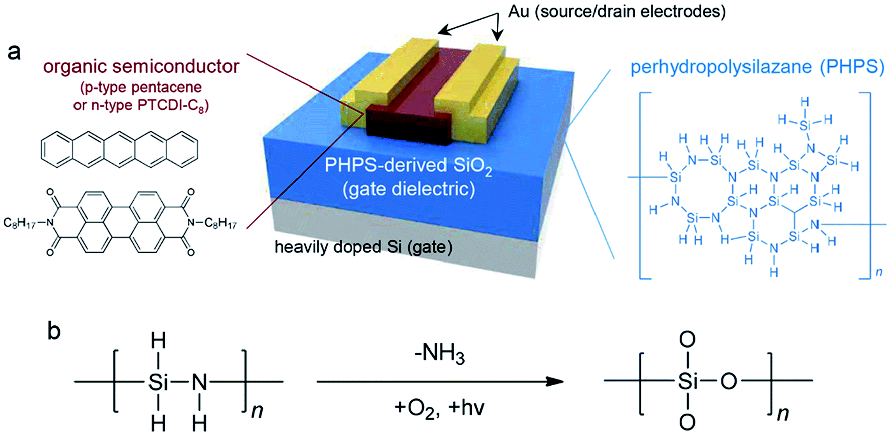 | ||
| Fig. 1 (a) Schematic structure of OFETs based on SiO2 gate dielectric layer derived from PHPS by IPL. The left panel shows the chemical structures of pentacene and PTCDI-C8, and the right panel shows the chemical structure of PHPS. (b) Curing mechanism of PHPS. | ||
Fig. 1b shows the curing mechanism of PHPS. PHPS can be converted to SiO2 through two different mechanisms: (i) hydrolysis and polycondensation in the presence of water28 and (ii) a photolytic process in the presence of oxygen.33 In the presence of water molecules under humid conditions, oxidation occurs by the hydrolysis of both the Si–N and the Si–H bonds, which leads to a release of gaseous ammonia and hydrogen and the formation of silanol groups. In the subsequent thermal condensation process, the silanol groups are transformed into SiO2 by the elimination of H2O. However, thermal treatment has some drawbacks in that high processing temperatures above 500 °C and long processing times-longer than 5 h-are required for complete conversion of PHPS to SiO2 without the formation of intermediates such as silanol groups. This process is similar to the typical sol–gel reaction. In the case of the photolytic process, high-energy UV irradiation causes dissociation of chemical bonds and generation of ozone molecules (O3) and oxygen radicals (O, one-dimensional). This results in the direct substitution of a Si atom with activated oxygen and, finally, the formation of SiOx. IPL irradiation induces a nuclear reaction by accelerating charged particles with kinetic energy, which is stronger than the irradiation by an ordinary UV lamp. IPL irradiation uses a photon energy of 4.43–12.4 eV with a wavelength range of 100–280 nm, which corresponds to the UV-C range in the electromagnetic spectrum. The high-energy UV photons promote the dissociation of the Si–N bond and the formation of Si free radicals and consequently form SiOx through oxidation with activated oxygen. The IPL irradiation method drastically reduces the conversion time (<2 h), which consequently results in an improvement in the productivity compared to the thermal annealing method, which requires high temperatures (>500 °C) and long processing times (>5 h). Furthermore, this room-temperature process enables the deposition of materials on plastic substrates with low glass transition temperatures.
The chemical structure of the PHPS-derived SiO2 films was investigated by FT-IR spectroscopy. Fig. 2 shows the FT-IR absorption spectra of the PHPS-derived SiO2 films and their gate dielectric properties. The as-coated PHPS film showed three characteristic absorption bands, which were attributed to the N–H, Si–H, and Si–N bonds.28,36–38 In the spectrum, the absorption bands positioned at 1178 and 3372 cm−1 corresponded to the bending and stretching modes of the N–H bond, respectively. The absorption peak at 2165 cm−1 corresponded to the stretching vibration of the Si–H bond, and the absorption peaks at 920 and 840 cm−1 were attributed to the stretching vibrations of Si–N in the Si–N–Si bond. The curing condition of PHPS was systematically optimized by varying both the number of intense pulses and the applied voltage, as shown in Fig. 2a and b. Specifically, Fig. 2a shows the FT-IR spectra of the PHPS films prepared at various applied voltages. The number of intense pulses was fixed at 6000 counts. With an increase in the applied voltage of the IPL irradiation, the Si–N, Si–H, and N–H absorption bands decreased gradually and disappeared completely at 3.0 kV. Simultaneously, absorption peaks at 800 and 1170 cm−1, attributed to the stretching vibrations of the Si–O and Si–O–Si bonds appeared, respectively.36,39,40 In addition, a new absorption peak at 3670 cm−1 corresponding to the Si–OH bond–appeared at 3.0 kV, which was related to the undesirable dangling bonds formed during the conversion process.41 It could be concluded that the SiO2 network was formed by the hydrolysis of the Si–NH bonds and the subsequent formation of the Si–O bond. Subsequently, the number of intense pulses was increased to 8000 counts while maintaining the applied voltage at 3.0 kV. With an increase in the number of intense pulses, the stretching vibration of the Si–H bond at 2165 cm−1 decreased gradually, as shown in Fig. 2b. Although the absorption peak of the Si–OH bond disappeared completely at 8000 counts, microcracks were formed on the PHPS-derived SiO2 film (Fig. S1†) and the leakage current increased significantly (Fig. S2†). The FT-IR spectrum of the SiO2 film derived from IPL-converted PHPS was compared with that of a SiO2 film derived from PHPS by thermal treatment at 600 °C for 5 h, as shown in Fig. 2c. Both these FT-IR spectra were similar to each other in terms of the shape of the absorption peaks achieved by the different conversion methods. It is noteworthy that the PHPS films could be converted to SiO2 by IPL irradiation at room temperature, similar to what could be achieved via thermal treatment. However, it was considered that the electrical properties of the PHPS-derived SiO2 film would be affected by its subtle SiO2 lattice structure. Therefore, the PHPS-derived SiO2 films were prepared for use as a gate dielectric layer in OFETs under the optimized condition of 3.0 kV and 6000 counts achieved via systematic variation of the irradiation conditions.
 | ||
| Fig. 2 (a) FT-IR spectra of PHPS films prepared at various applied voltages during IPL irradiation. The number of counts was fixed at 6000. (b) FT-IR spectra of PHPS films prepared at various numbers of intense pulses of IPL. The applied voltage was fixed at 3.0 kV. (c) FT-IR spectra of SiO2 film derived from PHPS by IPL irradiation (3.0 kV and 6000 counts) and that derived from PHPS by thermal treatment (600 °C and 5 h). (d) Current density of PHPS films prepared at various applied voltages during IPL irradiation as a function of electric field. (e) Current density of PHPS films prepared at various applied voltages during IPL irradiation at 1.5 MV cm−1. (f) Specific capacitance of SiO2 film derived from PHPS by IPL irradiation (3.0 kV and 6000 counts). | ||
The leakage current densities of the SiO2 gate dielectric derived from IPL-converted PHPS were measured using the metal–insulator–metal (MIM) geometry, as shown in Fig. 2d. The PHPS film converted at 1 kV showed a huge leakage current even under an electric field lower than 0.1 MV cm−1. With an increase in the applied voltage during the IPL irradiation to 2.5 kV, the leakage current reduced gradually and then saturated above 2.5 kV. For example, the PHPS-derived SiO2 film converted at 1.5 kV showed a leakage current density of 7.9 × 10⁻¹¹ A cm−2 at 1.5 MV cm−1 and that converted at 2.5 kV showed a leakage current density that was more than one order of magnitude lower, 3.0 × 10⁻¹² A cm−2, at 1.5 MV cm−1. Fig. 2e shows the leakage current density of the PHPS-derived SiO2 film at 1.5 MV cm−1 as a function of the applied voltage. A further increase in the voltage to up to 3.0 kV improved the electrical stability at high electric fields above 2 MV cm−1. This leakage current level was superior compared with those of typical polymer gate dielectrics such as poly(methyl methacrylate), polystyrene, and fluorinated polymers.42–46 As a result, the PHPS-derived SiO2 film at 3.0 kV and 6000 counts were chosen as a gate dielectric layer for fabricating the OFETs. Fig. 2f shows the specific capacitance of the optimized PHPS-derived SiO2 film as a function of frequency. The film thickness was around 525 nm (Fig. S3†). The capacitance value was measured to be 3.48 nF cm−2 at 100 Hz, and it showed a weak dependence on frequency. The dielectric constant (k) calculated from the capacitance and thickness was around 3.8 at 1 MHz, which was identical to that of a thermally grown SiO2 layer (k ∼ 3.9). It should be noted that PHPS was fully converted to SiO2 by the IPL irradiation at room temperature and that this film exhibited high electrical stability.
Fig. 3 shows the device performance of OFETs with the SiO2 gate dielectric derived from IPL-converted PHPS. The electrical properties of these OFETs were compared with those of an OFET with the SiO2 gate dielectric thermally derived from PHPS and an OFET with the thermally grown SiO2 gate dielectric. Fig. 3a shows the output characteristics (drain current (ID) versus drain voltage (VD)) of the pentacene OFET with the SiO2 gate dielectric derived from IPL-converted PHPS at various gate voltages (VG). The curves showed the gate modulation of ID in both the linear regime and the saturation regime. The left panel of Fig. 3b shows the transfer characteristics (ID–VG) of the pentacene OFET with the SiO2 gate dielectric derived from IPL-converted PHPS at VD = −40 V. The pentacene device turned on sharply near 0 V and its ID increased with a decrease in VG in the negative direction, which is a characteristic feature of p-type operation of a transistor. The carrier mobility (μ) in the saturation regime was evaluated according to the formula ID = CSμW(VG − VTH)2/(2L), where L and W are the length and width, respectively, of the device channel; CS is the specific capacitance of the gate dielectric (3.48 nF cm−2 for IPL-converted PHPS), and VTH is the threshold voltage.47,48 The μ value of the pentacene OFET with the SiO2 gate dielectric derived from IPL-converted PHPS was 0.16 (±0.01) cm2 V−1 s−1. It should be noted that this value was comparable to those of the OFETs with the SiO2 gate dielectric thermally derived from PHPS (0.14 (±0.01) cm2 V−1 s−1) and the thermally grown SiO2 gate dielectric (0.15 (±0.01) cm2 V−1 s−1) (see Fig. S4†). The on–off current ratio was around 106 and VTH was around −50 V. The device parameters, including μ, the on–off current ratio, and VTH, are summarized in Fig. 3c.
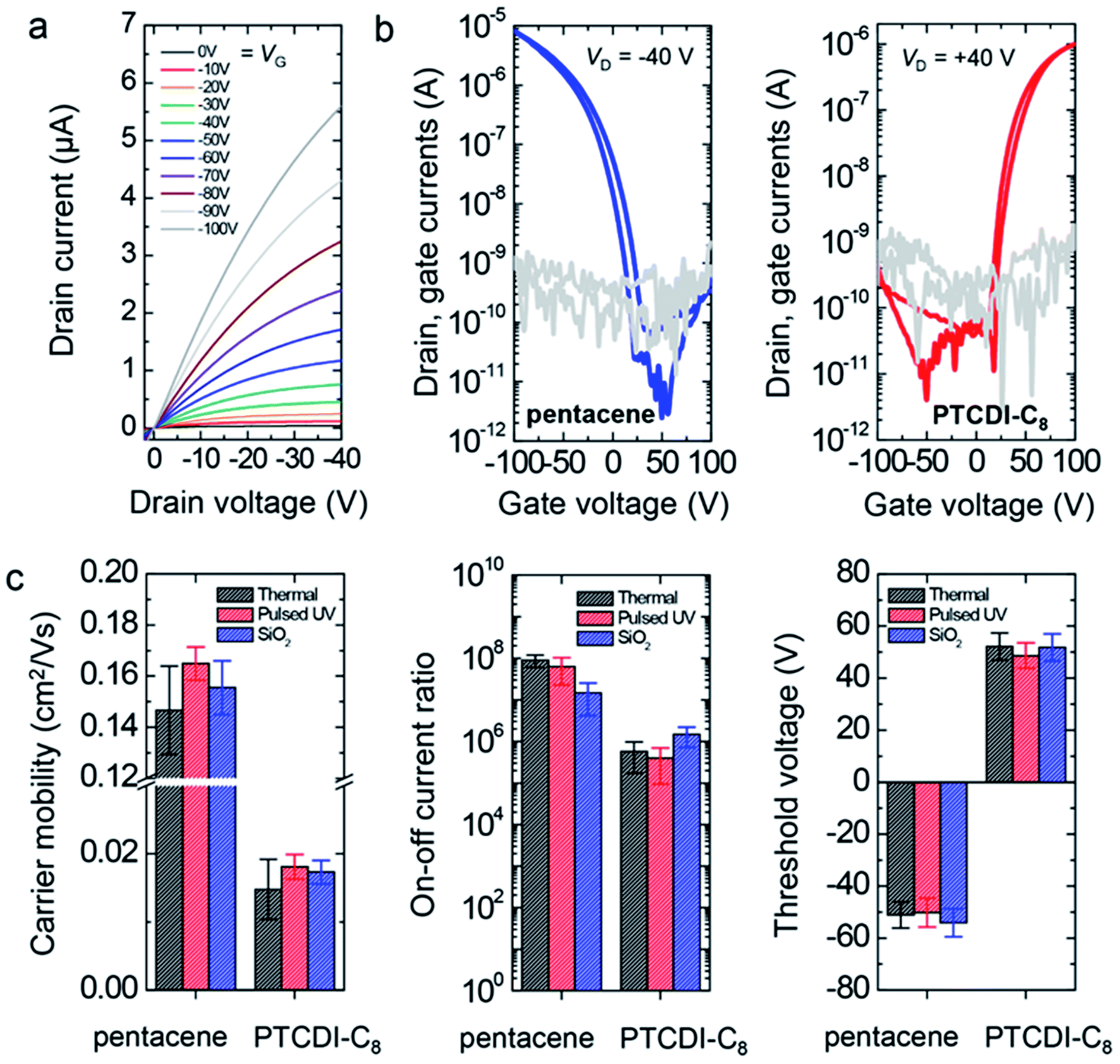 | ||
| Fig. 3 (a) Output characteristics of p-type pentacene OFET with SiO2 film derived from PHPS by IPL irradiation (3.0 kV and 6000 counts). (b) Transfer characteristics of p-type pentacene (left) and n-type PTCDI-C8 (right) OFETs with SiO2 film derived from PHPS by IPL irradiation (3.0 kV and 6000 counts). (c) Carrier mobility, on–off current ratio, and threshold voltage of OFETs with SiO2 film derived from PHPS by IPL irradiation (3.0 kV and 6000 counts), SiO2 film derived from PHPS by thermal treatment (600 °C and 5 h), and commercial thermally grown SiO2 film. | ||
Additionally, PTCDI-C8 was utilized as the n-type semiconductor counterpart to pentacene utilized as the p-type semiconductor. The right panel of Fig. 3b shows the transfer characteristics of the PTCDI-C8 OFET with the SiO2 gate dielectric derived from IPL-converted PHPS at VD = +40 V. In contrast to ID of the pentacene OFET, that of the PTCDI-C8 OFET increased with an increase in VG in the positive direction, which is a direct signature of the n-type operation of a transistor (also see Fig. S5†). The PTCDI-C8 OFET with the SiO2 gate dielectric derived from IPL-converted PHPS showed electron mobility of 0.02 (±0.01) cm2 V−1 s−1. The lower carrier mobility of the n-type OFET than of the p-type OFET may be attributed to the fact that electrons were easily trapped at the charge-trap sites formed at the interface between the semiconductor layer and the gate dielectric layer. However, this value was comparable to those of the OFETs with the SiO2 gate dielectric thermally derived from PHPS (0.01 (±0.018) cm2 V−1 s−1) and the thermally grown SiO2 gate dielectric (0.02 (±0.002) cm2 V−1 s−1). The device showed an on–off current ratio of around 105 and VTH of around +50 V. A slight hysteresis between the forward and reverse sweeps was observed in both OFETs because of the generation of charge traps from the Si–OH groups formed during the conversion process (see Fig. 2a). The gate leakage currents of both the p-type and the n-type OFETs were also monitored during measurement of the transfer curves. It is noteworthy that both these devices showed a gate leakage current of around 10−10 A, which was comparable to that of the device with the SiO2 gate dielectric thermally derived from PHPS.
Finally, a complementary inverter, which is the most basic component of logic circuits, was constructed by integrating a p-type pentacene OFET and an n-type PTCDI-C8 OFET with the SiO2 gate dielectric derived from IPL-converted PHPS (Fig. 4a). The p-type OFET was connected to the supply electrode, whereas the n-type OFET was connected to the ground. Both these OFETs shared the same input and output terminals. Fig. 4b shows the corresponding circuit diagram. Fig. 4c shows the voltage transfer characteristics of the constructed complementary inverter at four different VDD values. The device exhibited ideal rail-to-rail output swing. When a low input voltage (VIN) was applied, the p-type OFET turned on but the n-type OFET turned off. Thus, the output voltage (VOUT) was the same as the applied VDD (10, 20, 30, or 40 V). As VIN increased, the p- and n-type OFETs turned off and on, respectively. VOUT approached 0 V. Fig. 4d shows the static gain–which refers to the absolute value of dVOUT/dVIN–of the inverter as a function of VIN. The device showed a maximum inverter gain of 1.8 at VDD = 40 V.
 | ||
| Fig. 4 (a) Schematic illustration and (b) circuit diagram of complementary inverter with SiO2 gate dielectric derived from PHPS by IPL irradiation (3.0 kV and 6000 counts). (c) Voltage transfer characteristics and (d) signal gain of complementary inverter. | ||
Conclusion
We fabricated OFETs and a complementary inverter including a SiO2 gate dielectric layer derived from PHPS by IPL irradiation. The spin-coated PHPS was completely converted to SiO2 by optimizing both the number of intense pulses and the applied voltage. PHPS-derived SiO2 films at 3.0 kV and 6000 counts were utilized as a gate dielectric layer in p-type pentacene and n-type PTCDI-C8 OFETs. The gate dielectric properties of the PHPS-derived SiO2 films were systematically investigated. The resulting SiO2 films were successfully applied as a gate dielectric layer in p-type pentacene and n-type PTCDI-C8 OFETs. The resulting OFETs showed good electrical properties, such as carrier mobilities of 0.16 (±0.01) cm2 V−1 s−1 (for the pentacene OFET) and 0.02 (±0.01) cm2 V−1 s−1 (for the PTCDI-C8 OFET) and an on–off current ratio larger than 105, which were comparable to those of OFETs with commercial thermally grown SiO2 and SiO2 thermally derived from PHPS. The use of IPL to convert PHPS to SiO2 for use as a gate dielectric layer in OFETs is expected to serve as a novel approach for the fabrication of large-area flexible electronics in the flexible device industry of the future.Experimental
Device fabrication
A Si wafer was used as the substrate. The substrate was cleaned in an ultrasonic bath sequentially with acetone, isopropanol, and deionized water for 10 min each. An 18 wt% PHPS solution (DNF Co., Ltd., Korea) in xylene was spin-coated onto the substrate at 5000 rpm for 30 s. The PHPS film was prebaked on a hotplate at 150 °C for 10 min to remove residual solvent. The resulting film was converted to SiO2 by using IPL (X-1000, xenon) at room temperature. The distance between light source and sample was 2.5 cm. A pulse width of 500 μs and pulse interval of 0.64 Hz were used in the air atmosphere. Both the number of intense pulses and the applied voltage were varied. The thickness of the PHPS-derived SiO2 film was around 524 nm. Pentacene and PTCDI-C8 films, each 40 nm in thickness, were deposited onto the gate dielectric at a rate of 0.1 Å s−1 by using a thermal evaporator. Finally, Au source and drain electrodes were thermally deposited through a shadow mask. The channel length (L) and width (W) were 100 and 1000 μm, respectively.Characterization
Fourier transform infrared (FT-IR) spectra of samples were recorded on a Nicolet 6700 FT-IR Spectrometer from ThermoElectron. Specific capacitances of gate dielectrics were measured with Agilent E-4980A LCR meter. Electrical properties of transistors were measured using Keithley 4200 semiconductor characterization system.Conflicts of interest
There are no conflicts to declare.Acknowledgements
This work was supported by the Ministry of Trade, Industry & Energy, Korea Institute for Advancement of Technology through the Encouragement Program for The Industries of Economic Cooperation Region (17-107-002, R0006234), the Center for Advanced Soft Electronics (CASE) under the Global Frontier Research Program (2013M3A6A5073177), and the Basic Science Research Program through the National Research Foundation of Korea (NRF) funded by the Ministry of Education (2017R1A2B2005790), Republic of Korea.References
- S. Reineke, F. Lindner, G. Schwartz, N. Seidler, K. Walzer, B. Lüssem and K. Leo, Nature, 2009, 459, 234–238 CrossRef CAS PubMed.
- J. Wu, H. A. Becerril, Z. Bao, Z. Liu, Y. Chen and P. Peumans, Appl. Phys. Lett., 2008, 92, 263302 CrossRef.
- G. Horowitz, Adv. Mater., 1999, 10, 365–377 CrossRef.
- M. J. Kim, A.-R. Jung, M. Lee, D. Kim, S. Ro, S.-M. Jin, H. D. Nguyen, J. Yang, K.-K. Lee, E. Lee, M. S. Kang, H. Kim, J.-H. Choi, B. Kim and J. H. Cho, ACS Appl. Mater. Interfaces, 2017, 9, 40503–40515 CrossRef CAS PubMed.
- C. B. Park, K. M. Kim, J. E. Lee, H. Na, S. S. Yoo and M. S. Yang, Org. Electron., 2014, 15, 3538–3545 CrossRef CAS.
- R. Rotzoll, S. Mohapatra, V. Olariu, R. Wenz, M. Grigas, K. Dimmler, O. Shchekin and A. Dodabalapur, Appl. Phys. Lett., 2006, 88, 123502 CrossRef.
- V. Subramanian, P. C. Chang, J. B. Lee, S. E. Molesa and S. K. Volkman, IEEE Trans. Compon. Packag. Technol., 2005, 28, 742–747 CAS.
- P. S. K. Amegadze and Y.-Y. Noh, J. Inf. Disp., 2014, 15, 213–229 CrossRef CAS.
- M. Lee, M. J. Kim, S. Ro, S. Choi, S.-M. Jin, H. D. Nguyen, J. Yang, K.-K. Lee, D. U. Lim, E. Lee, M. S. Kang, J.-H. Choi, J. H. Cho and B. Kim, ACS Appl. Mater. Interfaces, 2017, 9, 28817–28827 CrossRef CAS PubMed.
- N.-K. Kim, S.-Y. Jang, G. Pace, M. Caironi, W.-T. Park, D. Khim, J. Kim, D.-Y. Kim and Y.-Y. Noh, Chem. Mater., 2015, 27, 8345–8353 CrossRef CAS.
- X.-H. Zhang, B. Domercq, X. Wang, S. Yoo, T. Kondo, Z. L. Wang and B. Kippelen, Org. Electron., 2007, 8, 718–726 CrossRef CAS.
- Y. Su, C. Wang, W. Xie, F. Xie, J. Chen, N. Zhao and J. Xu, ACS Appl. Mater. Interfaces, 2011, 3, 4662–4667 CrossRef CAS.
- S. Ono, R. Häusermann, D. Chiba, K. Shimamura, T. Ono and B. Batlogg, Appl. Phys. Lett., 2014, 104, 013307 CrossRef.
- H. Watanabe, M. Saitoh, N. Ikarashi and T. Tatsumi, Appl. Phys. Lett., 2004, 85, 449–451 CrossRef CAS.
- F. Iacopi, Z. Tőkei, Q. T. Le, D. Shamiryan, T. Conard, B. Brijs, U. Kreissig, M. Van Hove and K. Maex, J. Appl. Phys., 2002, 92, 1548–1554 CrossRef CAS.
- C. M. Perkins, B. B. Triplett, P. C. McIntyre, K. C. Saraswat, S. Haukka and M. Tuominen, Appl. Phys. Lett., 2001, 78, 2357–2359 CrossRef CAS.
- A.-D. Li, Q.-Y. Shao, H.-Q. Ling, J.-B. Cheng, D. Wu, Z.-G. Liu, N.-B. Ming, C. Wang, H.-W. Zhou and B.-Y. Nguyen, Appl. Phys. Lett., 2003, 83, 3540–3542 CrossRef CAS.
- M. M. Frank, G. D. Wilk, D. Starodub, T. Gustafsson, E. Garfunkel, Y. J. Chabal, J. Grazul and D. A. Muller, Appl. Phys. Lett., 2005, 86, 152904 CrossRef.
- E. P. Gusev, C. Cabral, M. Copel, C. D'Emic and M. Gribelyuk, Microelectron. Eng., 2003, 69, 145–151 CrossRef CAS.
- M. D. Cheng, T. Luoh, C. T. Su, T. H. Yang, K. C. Chen and C. Y. Lu, Thin Solid Films, 2008, 516, 8726–8730 CrossRef CAS.
- D. Hishitani, M. Horita, Y. Ishikawa, H. Ikenoue and Y. Uraoka, Jpn. J. Appl. Phys., 2017, 56, 056503 CrossRef.
- W. Kang, G. An, M. J. Kim, W. H. Lee, D. Y. Lee, H. Kim and J. H. Cho, J. Phys. Chem. C, 2016, 120, 3501–3508 CrossRef CAS.
- M. J. Kim, Y. M. Heo and J. H. Cho, Org. Electron., 2017, 43, 41–46 CrossRef CAS.
- R. Usuda, K. Uchida and S. Nozaki, Appl. Phys. Lett., 2015, 107, 182903 CrossRef.
- H. Kozuka, K. Nakajima and H. Uchiyama, ACS Appl. Mater. Interfaces, 2013, 5, 8329–8336 CrossRef CAS PubMed.
- J. Song, D. Wang, L. Hu, X. Huang and Y. Chen, Appl. Surf. Sci., 2018, 455, 771–779 CrossRef CAS.
- K. Kamiya, T. Tange and T. Hashimoto, Res. Rep. Fac. Eng., Mie Univ., 2001, 26, 23–31 CAS.
- A. Morlier, S. Cros, J.-P. Garandet and N. Alberola, Thin Solid Films, 2012, 524, 62–66 CrossRef CAS.
- K. Kamiya, A. Oka, H. Nasu and T. Hashimoto, J. Sol-Gel Sci. Technol., 2000, 19, 495–499 CrossRef CAS.
- T. Kubo and H. Kozuka, J. Ceram. Soc. Jpn., 2006, 114, 517–523 CrossRef CAS.
- T. Tanaka, K. Hanaoka, M. Yamaguchi, T. Shindo, K.-H. Kunzelmann and T. Teranaka, Dent. Mater., 2011, 30, 170–175 CrossRef CAS.
- J.-S. Lee, J.-H. Oh, S.-W. Moon, W.-S. Sul and S.-D. Kim, Electrochem. Solid-State Lett., 2010, 13, H23–H25 CrossRef CAS.
- L. Prager, A. Dierdorf, H. Liebe, S. Naumov, S. Stojanović, R. Heller, L. Wennrich and M. R. Buchmeiser, Chem.–Eur. J., 2007, 13, 8522–8529 CrossRef CAS PubMed.
- Y. Naganuma, S. Tanaka, C. Kato and T. Shindo, J. Ceram. Soc. Jpn., 2004, 112, 599–603 CrossRef CAS.
- T. Ohishi, Y. Yamazaki and T. Nabatame, Frontiers in Nanoscience and Nanotechnology, 2016, 2, 149–154 Search PubMed.
- Z. Zhang, Z. Shao, Y. Luo, P. An, M. Zhang and C. Xu, Polym. Int., 2015, 64, 971–978 CrossRef CAS.
- K. Wang, M. Günthner, G. n. Motz, B. D. Flinn and R. K. Bordia, Langmuir, 2013, 29, 2889–2896 CrossRef CAS PubMed.
- K. Wang, X. Zheng, F. S. Ohuchi and R. K. Bordia, J. Am. Ceram. Soc., 2012, 95, 3722–3725 CrossRef CAS.
- K. Nakajima, H. Uchiyama, T. Kitano and H. Kozuka, J. Am. Ceram. Soc., 2013, 96, 2806–2816 CrossRef CAS.
- H. S. Lee, K. Park, J.-D. Kim, T. Han, K. H. Ryu, H. S. Lim, D. R. Lee, Y.-J. Kwark and J. H. Cho, J. Mater. Chem., 2011, 21, 6968–6974 RSC.
- Y. Jeong, C. Pearson, H.-G. Kim, M.-Y. Park, H. Kim, L.-M. Do and M. C. Petty, ACS Appl. Mater. Interfaces, 2016, 8, 2061–2070 CrossRef CAS PubMed.
- H. S. Lee, K. Park, J.-D. Kim, T. Han, K. H. Ryu, H. S. Lim, D. R. Lee, Y.-J. Kwark and J. H. Cho, J. Mater. Chem., 2011, 21, 6968–6974 RSC.
- D. K. Hwang, C. Fuentes-Hernandez, J. Kim, W. J. Potscavage Jr, S. J. Kim and B. Kippelen, Adv. Mater., 2011, 23, 1293–1298 CrossRef CAS PubMed.
- X. Cheng, M. Caironi, Y.-Y. Noh, J. Wang, C. Newman, H. Yan, A. Facchetti and H. Sirringhaus, Chem. Mater., 2010, 22, 1559–1566 CrossRef CAS.
- T. Umeda, D. Kumaki and S. Tokito, Org. Electron., 2008, 9, 545–549 CrossRef CAS.
- C.-Y. Yang, J.-S. Chen and S. L.-C. Hsu, J. Electrochem. Soc., 2006, 153, F120–F125 CrossRef CAS.
- C. Luo, A. K. K. Kyaw, L. A. Perez, S. Patel, M. Wang, B. Grimm, G. C. Bazan, E. J. Kramer and A. J. Heeger, Nano Lett., 2014, 14, 2764–2771 CrossRef CAS PubMed.
- M. S. Kang and C. D. Frisbie, ChemPhysChem, 2013, 14, 1547–1552 CrossRef CAS PubMed.
Footnote |
| † Electronic supplementary information (ESI) available. See DOI: 10.1039/c8ra09831j |
| This journal is © The Royal Society of Chemistry 2019 |