
 Open Access Article
 This Open Access Article is licensed under a Creative Commons Attribution-Non Commercial 3.0 Unported Licence
Formation of an MoTe2 based Schottky junction employing ultra-low and high resistive metal contacts†
Sikandar Aftaba,
Muhammad Waqas Iqbal *b,
Amir Muhammad Afzala,
M. Farooq Khana,
Ghulam Hussainb,
Hafiza Sumaira Waheedb and
Muhammad Arshad Kamranc
*b,
Amir Muhammad Afzala,
M. Farooq Khana,
Ghulam Hussainb,
Hafiza Sumaira Waheedb and
Muhammad Arshad Kamranc
aDepartment of Physics and the Astronomy and Graphene Research Institute, Sejong University, Seoul 05006, Korea
bDepartment of Physics, Riphah Institute of Computing and Applied Sciences (RICAS), Riphah International University, 14 Ali Road, Lahore, Pakistan. E-mail: waqas.iqbal@riphah.edu.pk
cDepartment of Physics, College of Science, Majmaah University, PO Box No. 1712, Al-Zulfi 11932, Saudi Arabia
First published on 29th March 2019
Abstract
Schottky-barrier diodes have great importance in power management and mobile communication because of their informal device technology, fast response and small capacitance. In this research, a p-type molybdenum ditelluride (p-MoTe2) based Schottky barrier diode was fabricated using asymmetric metal contacts. The MoTe2 nano-flakes were mechanically exfoliated using adhesive tape and with the help of dry transfer techniques, the flakes were transferred onto silicon/silicon dioxide (Si/SiO2) substrates to form the device. The Schottky-barrier was formed as a result of using ultra-low palladium/gold (Pd/Au) and high resistive chromium/gold (Cr/Au) metal electrodes. The Schottky diode exhibited a clear rectifying behavior with an on/off ratio of ∼103 and an ideality factor of ∼1.4 at zero gate voltage. In order to check the photovoltaic response, a green laser light was illuminated, which resulted in a responsivity of ∼3.8 × 10³ A W−1. These values are higher than the previously reported results that were obtained using conventional semiconducting materials. Furthermore, the barrier heights for Pd and Cr with a MoTe2 junction were calculated to be 90 meV and 300 meV, respectively. In addition, the device was used for rectification purposes revealing a stable rectifying behavior.
1. Introduction
Because of their unique semiconductive characteristics, transition metal dichalcogenides (TMDs), have been used for extensive applications in nanoelectronics such as photodetectors,1–3 and spin-field effect transistors.4 The TMDs have a band gap of around 1 to 2 eV,5,6 and demonstrate fascinating electrical and optical properties.7–10 Molybdenum ditelluride (MoTe2) can be reduced to a monolayer or a few layers from its bulk form using adhesive tape through mechanical exfoliation.10 As found from previous reports, MoTe2 in its bulk form shows an indirect band gap of 0.88 eV, whereas its monolayer has a direct band-gap of 1.02 eV.8,11,12 The mobility for few-layered MoTe2 lies in the range of 0.2–40 cm2 V−1 s−1.13–16 Furthermore, use of MoTe2 has been shown to be favorable for many applications in environmental sensing, light emitting diodes and photosensors.17,18The two-dimensional (2D) material-based junctions have shown outstanding properties such as optical absorption, charge transportation and band alignment for optoelectronic and electronic applications.19,20 Until now, the study has mainly been based on heterojunctions comprising p–n junctions for practical uses of 2D materials, however semiconductor/metal Schottky barrier diodes (SBD) have not been studied extensively.21,22 The SBD is formed by a contact effect of metal and a semiconductive material which is the simplest structure amongst modern electronic devices.23 The SBDs have been shown to be promising for applications in electronic devices, for example, as photodiodes, power diodes, sensors, and integrated circuits.24,25 Schottky-barrier diodes have great importance in power management and mobile communications because of their informal device technology, fast response and small capacitance.26,27 In particular, Schottky diodes are majority carrier devices and because they are single carrier devices, they have advantages because of the junction diode which is a bipolar-device.
The interface properties of metal and semiconductor are influenced by the conductivity type of the charge carrier. The metal and semiconductor interface be either a rectifying type or an ohmic type, and is roughly dependent on the work function values of them. For example, a semiconductor material with n-type conductivity would show rectifying behavior with metals having greater work function values and show ohmic behavior with those having low work function values. However, semiconductors with p-type conductivity exhibit the opposite characteristics. The Schottky barrier because of a difference of Fermi level of the semiconductor and the work function of the metal, play an important role to determine the performance of a diode.28–30
In this research, the MoTe2 based field effect transistor (FET) is formed by using asymmetric metals contacts chromium/gold (Cr/Au) and palladium/gold (Pd/Au) to understand the charge carrier transport and the interface characteristics at the junction. It is found that MoTe2 forms an ohmic contact with Pd/Au whereas a Schottky barrier is observed with Cr/Au. In addition, an excellent photo response and gate-dependent behavior was found for the Schottky diode. A rectification ratio of up to 103 was calculated for the device. Furthermore, traditional thermionic emission theory was applied to determine the values of the Schottky barrier heights for individual metal contacts. The results obtained suggested that there would be useful technological applications for the Schottky diodes based on MoTe2.
2. Experimental
Natural bulk crystals of p-type molybdenum ditelluride (p-MoTe2) were exfoliated with adhesive tape and a dry transfer technique was used to transfer the flakes onto silicon/silicon dioxide (Si/SiO2) substrates with the help of a transparent poly(dimethylsiloxane) (PDMS) stamp. Multilayered p-MoTe2 nano-flakes were identified using Raman spectroscopy, optical microscopy and the results obtained were also confirmed using atomic force microscopy (AFM). Electrodes were made using e-beam lithography by depositing Pd/Au (8/10 nm) and Cr/Au (8/10 nm), onto the p-MoTe2 FET. The electrical transport measurements both at room and low temperatures were performed using the semiconductor characterization systems, Keithley 2400 Source Meter and Keithley 6485 Picoammeter.3. Results and discussion
The device is illustrated schematically in Fig. 1a and the optical image of the device is shown in Fig. 1b. The p-MoTe2 nano-flakes were exfoliated from their bulk form and using a dry transfer technique with a PDMS stamp were transferred onto the Si/SiO2 substrate. Fig. S1(a) (ESI†) shows the typical AFM image of p-MoTe2 FET on the SiO2 substrate. In addition the height profile for p-MoTe2 flakes with a thickness of ∼8 nm from the AFM image was obtained, and the results are shown in Fig. S1(b) (ESI†). Fig. S3 (ESI†) shows the Raman spectra of few-layer p-MoTe2 obtained using an excitation laser with a wavelength of 514 nm. Three peaks of MoTe2 were observed: A1g mode at ∼173.5 cm−1, E12g mode at ∼235.2 cm−1, and B12g mode at ∼290.8 cm−1.1 | ||
| Fig. 1 (a) Schematic illustration of the MoTe2 Schottky diode. (b) Optical microscope image of the device. (c) Band profile of Pd/MoTe2/Cr. (d) Transfer characteristics of p-MoTe2 with Pd/Au and Cr/Au FETs with Vds = 0.5 V. The ID–VD characteristics as a function of gate bias, (e) ultra-high resistive metal contact effect of p-MoTe2 with Cr/Au, and (f) ultra-low resistive ohmic metal contact behavior of MoTe2 with Pd/Au. | ||
Metals having larger values of work function are favorable for p-MoTe2 to form a shallow Schottky barrier whereas with low values of work function they show a greater barrier height.29,30 It was found that MoTe2 and the metal interface could be either an ohmic type or rectifying in nature depending on the work function of both the metals and the semiconductor. Pd (ϕ = 5.6 eV)31 and Cr (ϕ = 4.5 eV)32 were selected as the high and low work function metals, respectively, as shown in Fig. 1c.
Initially, the electrical performance of the device with source/drain Cr/Au and Pd/Au contacts was measured. For both configurations, p-MoTe2 showed strong p-type conduction as shown in Fig. 1d. The field-effect carrier mobility (μFE) was calculated for individual metal contacts using the following equation:
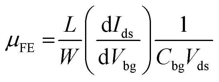
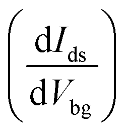 is the slope of the transfer characteristics. The hole mobility for the Cr/Au contacts was found to be 1.2 cm2 V−1 s−1 with a current on/off ratio of 103 whereas the hole mobility for the Pd/Au electrodes was found to be 7.0 cm2 V−1 s−1 with an on/off ratio of around 106 at Vds = 0.5 V. These findings revealed improved electrical characteristics when Pd/Au were contacted with MoTe2 rather than Cr/Au, which could be because of the formation of an ohmic contact and also be because of the use of a high work function metal (Pd with a work function ϕ = 5.6 eV).31 Also, in Fig. 1c it is clearly indicated in the band profile that the Fermi level of Pd is deeper than the Fermi level of MoTe2.
In addition, the ID–VD output characteristics were measured as a function of the back gate voltage (Vbg) which illustrated rectifying behavior for the Cr/Au metal contacts because of the formation of the Schottky barrier with p-MoTe2 (Fig. 1e), whereas ohmic contact is formed with Pd/Au because of linear I–V characteristics as shown in Fig. 1f.
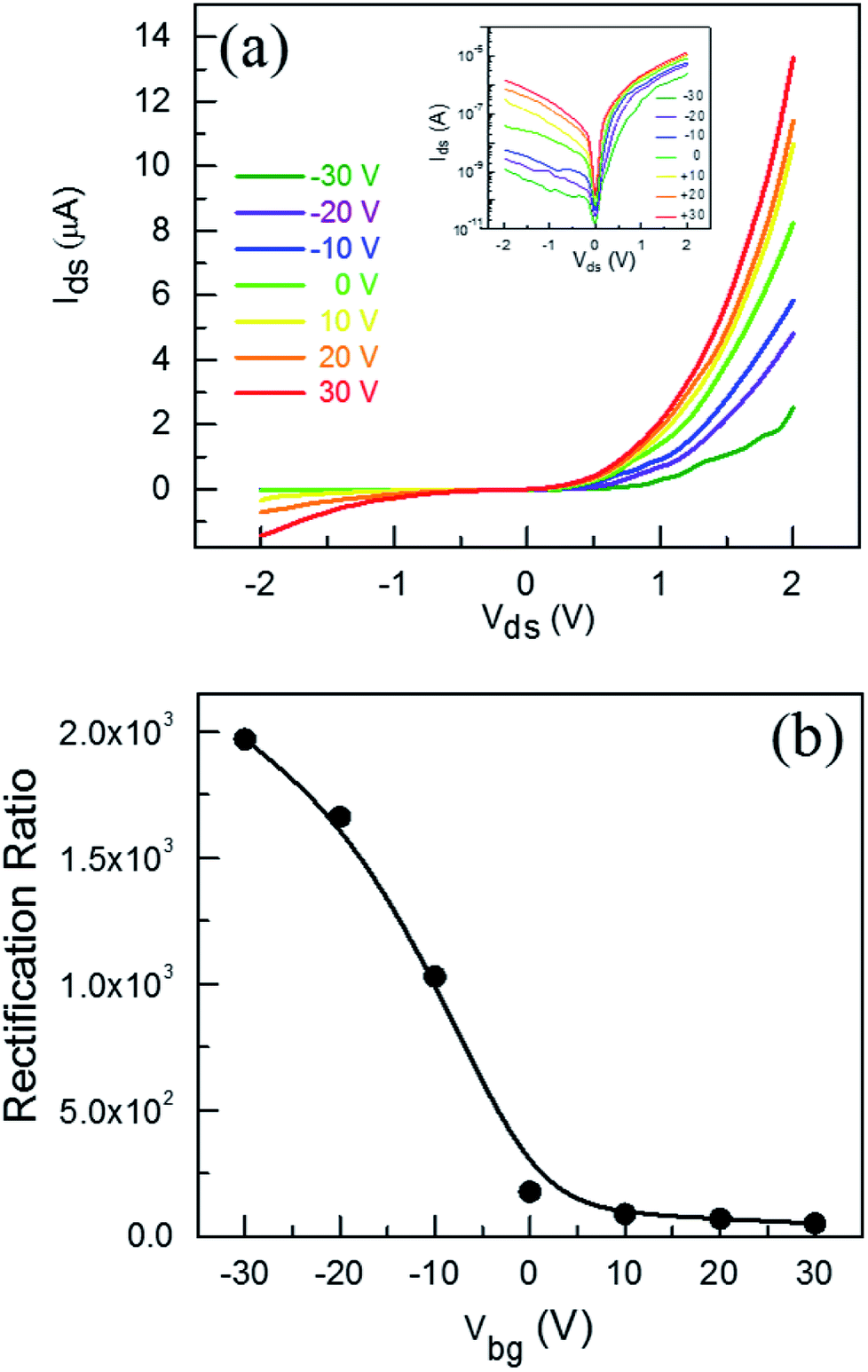
The output characteristics using Pd/Au and Cr/Au asymmetric electrodes showed a clear gate-dependent rectification behavior, particularly at negative gate bias voltages because of the high Schottky barrier height between Cr and MoTe2 as shown in Fig. 2a. The forward current increased steadily as a result of thinning the barrier. The rectification ratio could be defined as the ratio of reverse current (Ir) to forward current (If) at same ±Vds.33 The rectification ratio changed from 5.2 × 101 to 1.9 × 10³ with variation in gate bias as shown in Fig. 2b. The Schottky diode showed a better rectification ratio at a negative gate bias because of the reduction of the reverse leakage current because of greater band banding of the semiconductor with respect to the metal's Fermi level.21,22
 | ||
| Fig. 2 (a) Gate-dependent rectifying effect of MoTe2 Schottky junction between Cr/Au–Pd/Au contacts. (b) Rectification ratio as a function of the back gate of MoTe2 Schottky junction. | ||
Furthermore, the rectifying performance of the Schottky diode was studied by determining the ideality factor using the Shockley diode equation:34,35
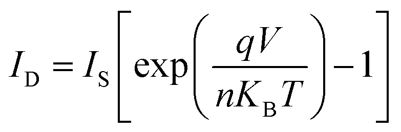
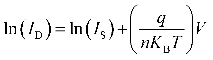
The slope from the plot of the natural logarithm of the diode current versus the applied voltage gives q/nKBT, which gives n. The lowermost value of n is found to be ∼1.4. The temperature dependent transfer characteristics were also measured, as shown in Fig. S2 (ESI†), to extract the Schottky barrier height (SBH) of Pd (ϕ = 5.6 eV)31 and Cr (ϕ = 4.5 eV).32 In this research, metal contacts were exclusively made of Pd and Cr and were directly adhered to the 2D semiconductor (MoTe2).
According to traditional thermionic emission theory, the following equation was used:36–38
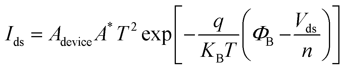
| ΦB = Φmetal − χsemi. |
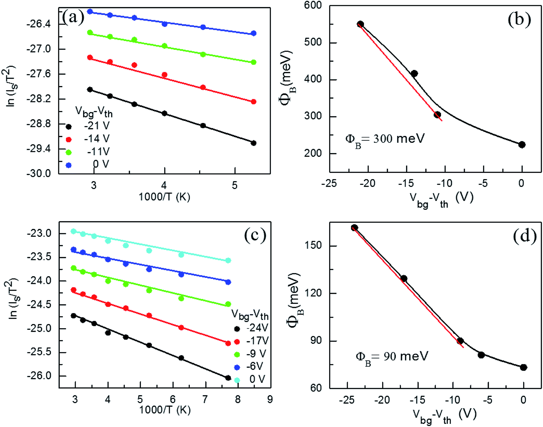 | ||
| Fig. 3 (a) Conventional Richardson plot ln(I/T2) versus 1000/T for Cr/Au metal contacts. (b) The potential barrier height at the MoTe2/Cr/Au junction as a function of Vbg–Vth. (c) Conventional Richardson plot ln(I/T2) versus 1000/T for Pd/Au metal contacts. (d) The potential barrier height at the MoTe2/Pd/Au junction as a function of Vbg–Vth. | ||
However, a number of semiconductors differ from the previously mentioned rule ever since the establishment of metal-induced gap states,39,40 which are occupied with electrons and shift the middle of the bandgap nearer to the Fermi level and this effect is known as Fermi level pinning.31,41 For example, p-MoTe2 had a stronger Fermi level pinning with Pd metal.31 However, the barrier height between Cr and MoTe2 was higher than that between Pd and MoTe2, which was the reason for the ohmic behavior of the MoTe2 and Pd/Au junction. Under forward biasing, if the Cr metal is connected with a negative bias, forward biasing would result in the holes being attracted to the interface as a result of a decrease in barrier height. Instead, under reverse biasing, if the Cr metal is connected with a positive terminal, reverse biasing would result in the holes being removed from the interface of the metal and semiconductor as a result of increased barrier height. So in the forwarding biased region the net current is larger, while in the reverse biasing region it is very low.
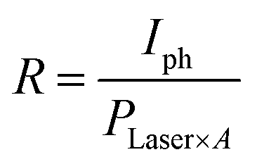
In addition, the photoresponse characteristics of the MoTe2 Schottky diode were also demonstrated. Under forwarding biasing the linear output characteristics were measured using asymmetric metal contacts, under light illumination with a green laser light with a wavelength of about 530 nm having a power of 1.2 mW cm−2 as shown in Fig. 4. At the forward biased region, the dark current was very low because of the ultra-high resistive metal contact between Cr and MoTe2. Upon illumination with green laser light, the photoresponsivity (R) of the Schottky junction was calculated using the equation:
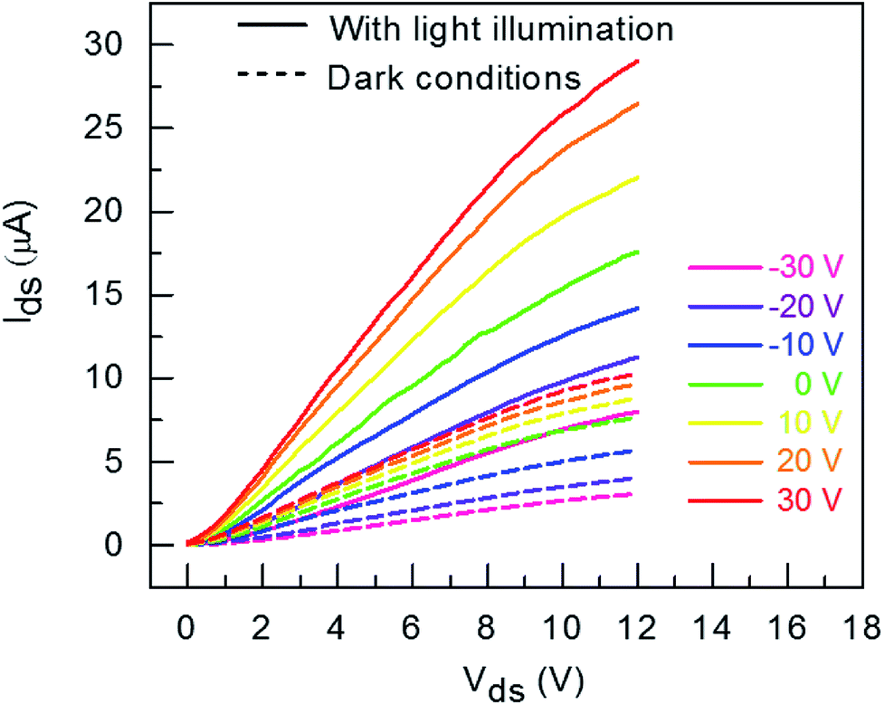 | ||
| Fig. 4 Output characteristics of the Schottky diode (Cr/Au–Pd/Au) with the positive bias as a function of gate bias. | ||
In addition, the Schottky diode was tested for the application of rectification, and which rectified output voltage signals by applying both AC square and sine waves. Fig. 5 presents the dynamic rectified VIn–VOut curves of the device at an external resistance of 1 MΩ by applying the AC sine and square input voltage signal sweeping from −5 to +5 V at 10 Hz.
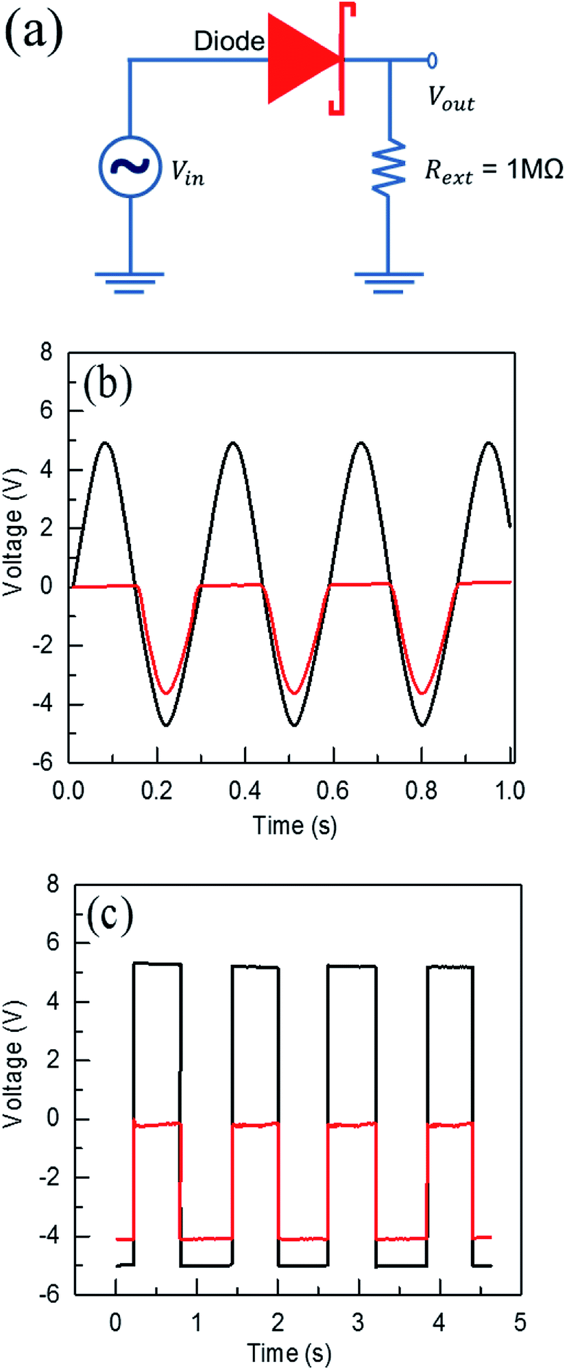 | ||
| Fig. 5 (a) Schematic illustration to demonstrate the dynamic rectification of a Schottky diode. Demonstration of rectified dynamic output of the Schottky diode by applying (b) AC sine and (c) square wave signals with a series resistor of resistance 1 MΩ. VIn = ±5 V at 10 Hz. | ||
4. Conclusions
In summary, a Schottky barrier diode was formed, based on a p-MoTe2 FET, which demonstrated excellent photo response and gate-dependent behavior. The Schottky diode showed a clear rectifying behavior with an on/off ratio reaching up to 103 and with an ideality factor of ∼1.4 at zero gate voltage. In order to check the photovoltaic response, the diode was illuminated with green laser light, and the responsivity was 3.8 × 10³ A W−1, which was higher than the previously reported values based on conventional semiconductor materials. The barrier heights for Pd and Cr with a MoTe2 junction were calculated to be 90 meV and 300 meV, respectively. In addition, the device was used for rectification and revealed stable rectifying behavior. The outcomes of this research can be applied in future electronics which require high speed and low noise performance.Conflicts of interest
There are no conflicts to declare.Acknowledgements
This work was funded by the Higher Education Commission (HEC) of Pakistan under the National Research Program for Universities (NRPU) (Project No. 7876). This research was also supported by the HEC of Pakistan under the Start-Up Research Grant Program (Project No. 1285).References
- O. Lopez-Sanchez, D. Lembke, M. Kayci, A. Radenovic and A. Kis, Nat. Nanotechnol., 2013, 8, 497–501 CrossRef CAS PubMed.
- C. Lan, C. Li, Y. Yin and Y. Liu, Nanoscale, 2015, 7, 5974–5980 RSC.
- N. Perea-López, A. L. Elías, A. Berkdemir, A. Castro-Beltran, H. R. Gutiérrez, S. Feng, R. Lv, T. Hayashi, F. López-Urías and S. Ghosh, Adv. Funct. Mater., 2013, 23, 5511–5517 CrossRef.
- J. Klinovaja and D. Loss, Phys. Rev. B: Condens. Matter Mater. Phys., 2013, 88, 075404 CrossRef.
- B. Radisavljevic, A. Radenovic, J. Brivio, I. V. Giacometti and A. Kis, Nat. Nanotechnol., 2011, 6, 147–150 CrossRef CAS PubMed.
- T. Georgiou, R. Jalil, B. D. Belle, L. Britnell, R. V. Gorbachev, S. V. Morozov, Y.-J. Kim, A. Gholinia, S. J. Haigh and O. Makarovsky, Nat. Nanotechnol., 2013, 8, 100–103 CrossRef CAS PubMed.
- S. Fathipour, N. Ma, W. Hwang, V. Protasenko, S. Vishwanath, H. Xing, H. Xu, D. Jena, J. Appenzeller and A. Seabaugh, Appl. Phys. Lett., 2014, 105, 192101 CrossRef.
- C. Ruppert, O. B. Aslan and T. F. Heinz, Nano Lett., 2014, 14, 6231–6236 CrossRef CAS PubMed.
- M. Yamamoto, S. T. Wang, M. Ni, Y.-F. Lin, S.-L. Li, S. Aikawa, W.-B. Jian, K. Ueno, K. Wakabayashi and K. Tsukagoshi, ACS Nano, 2014, 8, 3895–3903 CrossRef CAS PubMed.
- B. Chamlagain, Q. Li, N. J. Ghimire, H.-J. Chuang, M. M. Perera, H. Tu, Y. Xu, M. Pan, D. Xaio and J. Yan, ACS Nano, 2014, 8, 5079–5088 CrossRef CAS PubMed.
- I. G. Lezama, A. Arora, A. Ubaldini, C. Barreteau, E. Giannini, M. Potemski and A. F. Morpurgo, Nano Lett., 2015, 15, 2336–2342 CrossRef CAS PubMed.
- I. G. Lezama, A. Ubaldini, M. Longobardi, E. Giannini, C. Renner, A. B. Kuzmenko and A. F. Morpurgo, 2D Mater., 2014, 1, 021002 CrossRef.
- C. Pan, Y. Fu, J. Wang, J. Zeng, G. Su, M. Long, E. Liu, C. Wang, A. Gao and M. Wang, Adv. Electron. Mater., 2018, 4, 1700662 CrossRef.
- Y. F. Lin, Y. Xu, S. T. Wang, S. L. Li, M. Yamamoto, A. Aparecido-Ferreira, W. Li, H. Sun, S. Nakaharai and W. B. Jian, Adv. Mater., 2014, 26, 3263–3269 CrossRef CAS PubMed.
- D. H. Keum, S. Cho, J. H. Kim, D.-H. Choe, H.-J. Sung, M. Kan, H. Kang, J.-Y. Hwang, S. W. Kim and H. Yang, Nat. Phys., 2015, 11, 482 Search PubMed.
- S. Nakaharai, M. Yamamoto, K. Ueno, Y.-F. Lin, S.-L. Li and K. Tsukagoshi, ACS Nano, 2015, 9, 5976–5983 CrossRef CAS PubMed.
- Y. F. Lin, Y. Xu, C. Y. Lin, Y. W. Suen, M. Yamamoto, S. Nakaharai, K. Ueno and K. Tsukagoshi, Adv. Mater., 2015, 27, 6612–6619 CrossRef CAS PubMed.
- Y.-Q. Bie, G. Grosso, M. Heuck, M. M. Furchi, Y. Cao, J. Zheng, D. Bunandar, E. Navarro-Moratalla, L. Zhou and D. K. Efetov, Nat. Nanotechnol., 2017, 12, 1124 CrossRef CAS PubMed.
- Y. Deng, Z. Luo, N. J. Conrad, H. Liu, Y. Gong, S. Najmaei, P. M. Ajayan, J. Lou, X. Xu and P. D. Ye, ACS Nano, 2014, 8, 8292–8299 CrossRef CAS PubMed.
- W. Hu and J. Yang, J. Mater. Chem. C, 2017, 5, 12289–12297 RSC.
- A. Di Bartolomeo, A. Grillo, F. Urban, L. Iemmo, F. Giubileo, G. Luongo, G. Amato, L. Croin, L. Sun and S. J. Liang, Adv. Funct. Mater., 2018, 28, 1800657 CrossRef.
- A. Di Bartolomeo, F. Urban, M. Passacantando, N. McEvoy, L. Peters, L. Iemmo, G. Luongo, F. Romeo and F. Giubileo, Nanoscale, 2019, 11, 1538–1548 RSC.
- T.-Y. Oh, S. Woo Jeong, S. Chang, K. Choi, H. Jun Ha and B. Kwon Ju, Appl. Phys. Lett., 2013, 102, 021106 CrossRef.
- Y. Zhao, X. Xiao, Y. Huo, Y. Wang, T. Zhang, K. Jiang, J. Wang, S. Fan and Q. Li, ACS Appl. Mater. Interfaces, 2017, 9, 18945–18955 CrossRef CAS PubMed.
- J. Miao, S. Zhang, L. Cai and C. Wang, Adv. Electron. Mater., 2016, 2, 1500346 CrossRef.
- J. B. Soole and H. Schumacher, IEEE J. Quantum Electron., 1991, 27, 737–752 CrossRef CAS.
- S. Averin, R. Sachot, J. Hugi, M. De Fays and M. Ilegems, J. Appl. Phys., 1996, 80, 1553–1558 CrossRef CAS.
- M. Yang, K. Teo, W. Milne and D. Hasko, Appl. Phys. Lett., 2005, 87, 253116 CrossRef.
- M. Hughes, K. Homewood, R. Curry, Y. Ohno and T. Mizutani, Appl. Phys. Lett., 2013, 103, 133508 CrossRef.
- B. Ryu, Y. T. Lee, K. H. Lee, R. Ha, J. H. Park, H.-J. Choi and S. Im, Nano Lett., 2011, 11, 4246–4250 CrossRef CAS PubMed.
- C. Kim, I. Moon, D. Lee, M. S. Choi, F. Ahmed, S. Nam, Y. Cho, H.-J. Shin, S. Park and W. J. Yoo, ACS Nano, 2017, 11, 1588–1596 CrossRef CAS PubMed.
- N. Dhar, T. Chowdhury, M. Islam, N. Khan, M. Rashid, M. Alam, Z. Alothman, K. Sopian and N. Amin, Chalcogenide Lett., 2014, 11, 271–279 CAS.
- F. Liu, W. L. Chow, X. He, P. Hu, S. Zheng, X. Wang, J. Zhou, Q. Fu, W. Fu and P. Yu, Adv. Funct. Mater., 2015, 25, 5865–5871 CrossRef CAS.
- D. A. Neamen, Semiconductor physics and devices, McGraw-Hill, New York, 1997 Search PubMed.
- T. Banwell and A. Jayakumar, Electron. Lett., 2000, 36, 291–292 CrossRef.
- J. H. Lee, H. Z. Gul, H. Kim, B. H. Moon, S. Adhikari, J. H. Kim, H. Choi, Y. H. Lee and S. C. Lim, Nano Lett., 2017, 17, 673–678 CrossRef CAS PubMed.
- A. Allain, J. Kang, K. Banerjee and A. Kis, Nat. Mater., 2015, 14, 1195 CrossRef CAS PubMed.
- S. Das, H.-Y. Chen, A. V. Penumatcha and J. Appenzeller, Nano Lett., 2012, 13, 100–105 CrossRef PubMed.
- K.-A. Min, J. Park, R. M. Wallace, K. Cho and S. Hong, 2D Materials, 2016, 4, 015019 CrossRef.
- S. Picozzi, A. Continenza, G. Satta, S. Massidda and A. Freeman, Phys. Rev. B: Condens. Matter Mater. Phys., 2000, 61, 16736 CrossRef CAS.
- P. Bampoulis, R. Van Bremen, Q. Yao, B. Poelsema, H. J. Zandvliet and K. Sotthewes, ACS Appl. Mater. Interfaces, 2017,(46), 39860–39871 Search PubMed.
- M. M. Furchi, A. Pospischil, F. Libisch, J. Burgdörfer and T. Mueller, Nano Lett., 2014, 14, 4785–4791 CrossRef CAS PubMed.
- L. Ye, H. Li, Z. Chen and J. Xu, ACS Photonics, 2016, 3, 692–699 CrossRef CAS.
- A. Rochas, A. R. Pauchard, P.-A. Besse, D. Pantic, Z. Prijic and R. S. Popovic, IEEE Trans. Electron Devices, 2002, 49, 387–394 CrossRef CAS.
Footnote |
| † Electronic supplementary information (ESI) available. See DOI: 10.1039/c8ra09656b |
| This journal is © The Royal Society of Chemistry 2019 |