
 Open Access Article
 This Open Access Article is licensed under a Creative Commons Attribution-Non Commercial 3.0 Unported Licence
Morphology controlling of 〈111〉-3C–SiC films by HMDS flow rate in LCVD
Qingfang Xua,
Rong Tu a,
Qingyun Suna,
Meijun Yanga,
Qizhong Lib,
Song Zhang*a,
Lianmeng Zhanga,
Takashi Gotoa,
Hitoshi Ohmoric,
Ji Shiad,
Haiwen Liae,
Marina Kosinovaaf and
Basu Bikramjitag
a,
Qingyun Suna,
Meijun Yanga,
Qizhong Lib,
Song Zhang*a,
Lianmeng Zhanga,
Takashi Gotoa,
Hitoshi Ohmoric,
Ji Shiad,
Haiwen Liae,
Marina Kosinovaaf and
Basu Bikramjitag
aState Key Laboratory of Advanced Technology for Materials Synthesis and Processing, Wuhan University of Technology, 122 Luoshi Road, Wuhan 430070, People's Republic of China. E-mail: kobe@whut.edu.cn
bHubei Key Laboratory of Advanced Technology for Automotive Components, Wuhan University of Technology, Wuhan 430070, China
cInstitute of Physical and Chemical Research, 2-1 Hirosawa, Wako, Saitama 351-0198, Japan
dSchool of Materials and Chemical Technology, Tokyo Institute of Technology, Tokyo 152-8552, Japan
eInternational Research Centre for Hydrogen Energy, Kyushu University, Fukuoka 819-0395, Japan
fNikolaev Institute of Inorganic Chemistry, Russian Academy of Sciences Siberian Branch, 3 Acad. Lavrerntiev Pr., Novosibirsk, 630090, Russia
gCentre for BioSystems Science and Engineering, Indian Institute of Science, Bangalore 560012, Karnataka, India
First published on 18th January 2019
Abstract
Morphology of 〈111〉-oriented 3C–SiC films was transformed from mosaic to whisker to cauliflower-like with the increased flow rate (f) of hexametyldisilane (HMDS) in the process of laser chemical vapor deposition (LCVD). The SiC whiskers were naturally sharp hexagonal pyramids with average height of 250 nm and an aspect ratio in the range of 5 to 10, with a density of 1.3 × 108 mm−2. The influence mechanism of f on the surface morphology, as well as the growth mechanism of SiC whiskers, was discussed.
1. Introduction
3C–SiC films have previously been prepared by chemical vapor deposition (CVD), thermal CVD (TCVD) and plasma enhanced CVD (PECVD) using CH4 + SiH4, CH4 + SiCl4 and methyltrichlorosilane (CH3SiCl3).1 However, CH4 and intermediate Si–C–H–Cl compounds are explosive, and the latter and its Cl-containing by-products (mainly HCl) are corrosive. It is beneficial to avoid explosive and corrosive precursors for CVD process. Hexamethyldisilane (HMDS, Si(CH3)3–Si(CH3)3) has been employed in low pressure CVD (LPCVD) as a non-explosive and non-corrosive precursor; however, the resulting deposition rates of 3C–SiC films were only several μm h−1 or less.2The laser chemical vapour deposition (LCVD) method developed by our group was employed to prepare 3C–SiC films with a high deposition rate and high quality using HMDS as precursor.1,3,4 The properties of the catalysis, sensing applications and field emission are highly dependent on the surface morphology of films.5–8 However, little research has been performed on the effect of the flow rate of precursor on the surface morphology of 3C–SiC films prepared by LCVD. In this study, the influence of f on the microstructure in LCVD has been investigated. The formation mechanisms of surface morphologies were also discussed.
2. Experimental
A cold-wall type LCVD was constructed to prepare 3C–SiC films on single crystalline Si(111) (Hefei Kejing Materials Technology Co. Ltd., Hefei, China) substrates. 2500 standard cubic centimetre per minute (sccm) H2 gas (Wuhan Xiangyun Chemical Co., Ltd., Wuhan, China, 99.999%) was flowed into the chamber as a dilution gas. An enlarged diode continuous laser beam (InGaAlAs, wavelength = 1060 nm, 20 mm in diameter) was irradiated on the Si substrate. The deposition temperature (Tdep) was measured with an infrared pyrometer (CT laser; Optris, Berlin, Germany; 673–1873 K) focused on the substrate. Hexametyldisilane (HMDS, Tokyo Chemical Industry Co., Ltd., Tokyo, Japan, 98%) was vaporised at 298 K and carried into the CVD chamber by 25 sccm Ar gas (Wuhan Xiangyun Chemical Co., Ltd., Wuhan, China, 99.999%). Then, the total pressure and deposition time was 400 Pa and 10 min, respectively. More details of the experiments and LCVD apparatus are available in our previous works.1,3The crystal phase and out-plane orientation of the films were analysed by X-ray diffraction with a multipurpose attachment (XRD, Rigaku Ultima III, 40 kV, 40 mA; Tokyo, Japan) with Cu-Kα (wavelength, 0.15406 nm). For the in-plane orientation analyses, the elevation angle (α) was fixed at 70.5° for {111} reflection of face-centred cubic (fcc) structure, while the azimuth angle (β) varied from 0 to 360° with step of 1°. The surface and cross-section morphology were observed by field emission scanning electron microscopy (FESEM; FEI Quanta-250, Houston, TX; 20 kV). The microstructure was observed by transmission electron microscopy (TEM; JEOL JEM-2100, Tokyo, Japan; 200 kV).
3. Results and discussion
The XRD θ–2θ diffraction patterns of the films deposited at f = 1–3 sccm are displayed in Fig. 1(a). Only 3C–SiC (111) plane diffraction peak at 2θ = 35.6° was identified, indicating strong 〈111〉 preferred orientation. As f increased from 1 sccm to 3 sccm, the full width at half-maximum (FWHM) of 3C–SiC(111) diffraction peaks is increased from 0.383° to 0.485°. The peak broadening may be ascribed to the defects such as dislocations which are usually generated at high supersaturation. Fig. 1(b) shows the β-scan patterns corresponding to 3C–SiC {111} planes for the same films shown in Fig. 1(a). Two sets of {111} reflection peaks of intrinsic epitaxial domains and double position domains (DPDs), respectively, are identified in the β-scan pattern of the 3C–SiC film deposited at f = 1 sccm, indicating that the 3C–SiC film is epitaxial. The intrinsic epitaxial domains and Si substrate has the epitaxial relationship of SiC [1–10]//Si [1–10] and SiC [111]//Si [111]. DPDs rotate around a 180°-〈111〉 axis compared to intrinsic epitaxial domains. However, the films show random in-plane orientation at f = 2–3 sccm for no peak observed in the β-scan patterns. The increase of f to 2–3 sccm caused supersaturation of precursor, and thus led to SiC grains randomly grown on the surface of the Si substrate.9 | ||
| Fig. 1 XRD θ–2θ diffraction patterns (a) and β-scan patterns (b) of 3C–SiC films. | ||
Fig. 2 shows the surface and cross-section standard electron microscopy (SEM) micrograph of the films, which exhibit three different kinds of surface morphologies. At f = 1 sccm, the film shows mosaic-like surface morphology (Fig. 2(a)). The flat top of the grains was parallel to the (111) lattice plane, and the direction on the side of the top is parallel to the [110] azimuth, which is a typical morphology of epitaxial 〈111〉-3C–SiC.10,11 At f = 2 sccm, the film shows whisker-like surface morphology (Fig. 2(b)). A high density of SiC whiskers with diameters of approximately 40 nm were grown on the surface. The whiskers, with average height of 250 nm (standard deviation: 41 nm), average diameter of 45 nm (standard deviation: 11 nm), and aspect ratio in the range of 5–10, look like needles with sharp tips. The number density of the whiskers reached 1.3 × 108 mm−2. At f = 2 sccm, the appropriate supersaturation to enable the growth of SiC grain with relative low nucleus density and high growth rate, which was beneficial for the formation of whiskers.12 As f increased to 3 sccm, the film exhibited a cauliflower-like surface morphology (Fig. 2(c)) and dense cross-section (Fig. 2(f)). The high-level supersaturation of precursor was in favour of a high nucleus density, which was beneficial for the formation of two-dimensional continuous film.13
 | ||
| Fig. 2 Surface and cross-section SEM micrograph of 3C–SiC films deposited. | ||
The characterization of the films are often correlated with the kinetic controlling mechanism of the deposition process (i.e., either the chemical reaction regime (CRR) or the mass transfer regime (MTR)),1,14,15 and the transfer of CRR to MTR can be induced by the increase of supersaturation. Loumagne et al.14 suggest that the growth of the films with angular surface morphology is correlated with the CRR (reactive species can reach stable growth site which yields a well-crystallized deposition grains), whereas the film exhibiting irregular surface morphology is correlated with the MRT (reactive species cannot reach a stable growth site before being covered). At f = 1 sccm, SiC grains grew at a low level of supersaturation controlled by CRR, leading to the formation of SiC grains with angular shape, whereas SiC grains grew at a high level of supersaturation controlled by MRT, and thus the films exhibited cauliflower-like surface morphology at f = 3 sccm.
We observed that the whisker-like 3C–SiC has rarely been reported recently. In order to further understand the deposition mechanism of whisker-like film in LCVD, the cross-section of the film prepared at f = 2 sccm was observed by TEM, as shown in Fig. (3). The (111) lattice plane diffraction rings of the selected area electron diffraction (SAED) from the bottom, the middle and the top of the film are shown in Fig. 3(a). The presence of rings indicates the film is polycrystalline. The intensities of {111} plane diffraction spots along the growth direction are much higher than those in the other direction, indicating the film exhibits 〈111〉 preferred orientation. However, there are only two diffraction spots along the growth direction in the direction ring from the top of the film, indicating the top of film exhibiting a strong 〈111〉 preferred orientation. The growth rate of (111) plane is much higher than the other plane. The grains were randomly first, than grew competitively, and finally 〈111〉-oriented grains became dominant on the surface.1 Fig. 3(b) shows the high-resolution transmission electron microscopy (HRTEM) of SiC grains from the middle yellow square in the in Fig. 3(a). As shown in Fig. 3(b), SiC grains are surrounded by amorphous grain boundary phase. Fig. 3(c) shows the side-view TEM image of a single SiC whisker on the surface of the film. As Fig. 3(d) shows, the as-prepared whisker grew along the 〈111〉 direction, and there is a high density of twin boundaries (TBs) on the (111) plane. The average linear density of the TBs along the 〈111〉 direction reaches 1.25 × 107 cm−1 evaluated on the cross-sectional HRTEM images. HRTEM images taken from different parts of the whisker show the same atomic arrangement, indicating that the whisker is single crystal. As shown in Fig. 3(e), the cross-section of whiskers was hexagonal as indicated by the dashed circles, and thus it could be inferred that the whiskers were hexagonal pyramids. 3C–SiC is an fcc, and the Wuffe shape of 3C–SiC is a triangular pyramid.16 The triangular pyramid of twins rotated 60° around the 〈111〉 axis. The hexangular pyramid texture was generated when two sets of triangular pyramids reached over each other face to face as shown in the inset of Fig. 3(e), resulting from the abundant twins at the (111) plane.
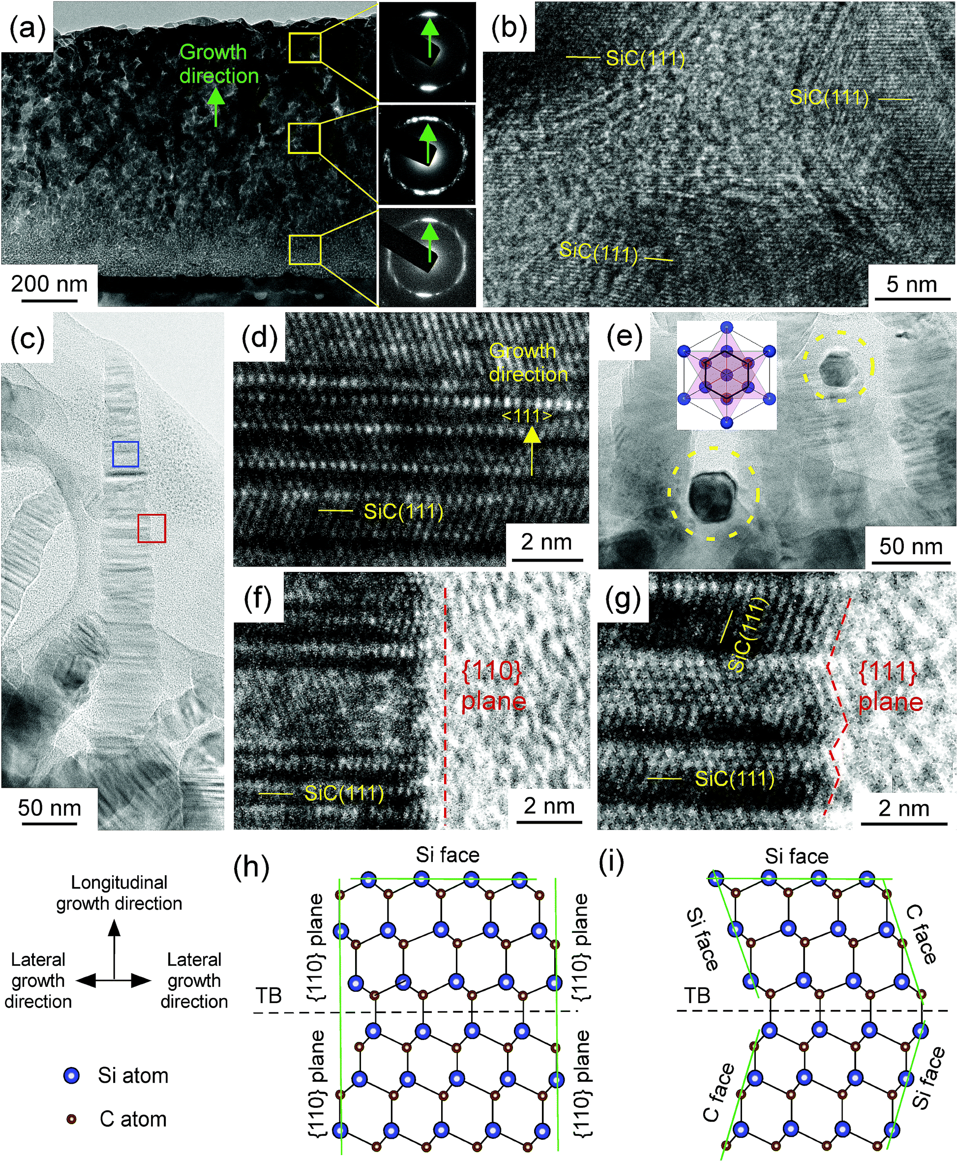 | ||
| Fig. 3 (a) Cross-section TEM image and SEAD of the 3C–SiC film prepared at f = 2 sccm; (b) HRTEM image from the green square in (a); (c) TEM image of a 3C–SiC whisker on the top of the film; (d) HRTEM image from the blue square in (c); (e) cross-section TEM image of SiC whisker; (f) and (g) HRTEM images of whisker edge from the red square in (c); (h) and (i) Schematic diagram of the atomic arrangement on the edge of whisker corresponding to (f) and (g), respectively. | ||
Xia et al.12 and Prakash et al.17 emphasized that the growth of one-dimensional structures from an isotropic medium is relatively simple and straightforward if the solid material has a highly anisotropic crystal, such as trigonal phase. 3C–SiC is characterised by isotropic crystal structure (fcc lattice), and symmetry breaking is required for anisotropic growth. However, no additional method or catalyser was introduced to break the isotropic symmetry for the growth of 3C–SiC whiskers in this study. Therefore, the atomic arrangements along the longitudinal growth and lateral growth direction were observed by HRTEM, as shown in Fig. 3(d), (f) and (g), to investigate the growth mechanism of whiskers in this study.
3C–SiC is a crystal with −43m symmetry, in which the {111} plane is a close-packed plane with the highest growth rate. The four {111} planes are Si-terminated and other four {111} planes are C-terminated, and the growth velocity of the Si-terminated {111} plane is much higher than the C-terminated {111} plane.16 Therefore, the fastest growing plane of 3C–SiC is the Si-terminated {111} plane. At f = 2 sccm, the Si-terminated {111} plane with the fastest growth rate continually decreased in area, and the surface with slower growth rate gradually dominated the morphology of crystals, which led to a 3C–SiC whisker with a sharp tip in the 〈111〉 direction.18
The edge of the whisker was observed by HRTEM, as shown in Fig. 3(f) and (g). The side of the whisker was mainly covered by the {110} plane, and a few were covered by the {111} plane, indicating that whisker grown in the lateral direction were mainly grown by stacking {110} lattice plane, and a few were grown by stacking {111} lattice plane. Fig. 3(h) and (i) depict the schematic of the atomic arrangements of Fig. 3(f) and (g). The growth velocity of the {110} plane is much lower than that of the {111} plane.16 However, a part of the side was covered by the {111} plane, half was the C-terminated {111} plane, and the other was the Si-terminated {111} plane. The growth velocity of the C-terminated {111} plane was much lower than that of the Si-terminated {111} plane.16 Therefore, the growth velocity of the {111} plane in lateral direction was also lower than the growth velocity of the Si-terminated {111} plane in the longitudinal direction. At f = 2 sccm, the growth velocity in the longitudinal direction was much higher than the growth velocity in the lateral direction, resulting in the formation of a whisker with a large aspect ratio.
4. Conclusions
〈111〉 preferred oriented 3C–SiC films were prepared by LCVD using HMDS as a single precursor. As f increased from 1 sccm to 3 sccm, the surface morphology of the films transferred from mosaic-like to whisker-like and then to cauliflower-like. The whiskers were sharp hexagonal pyramids with average height of 250 nm and an aspect ratio in the range of 5 to 10. The number density of the whiskers reached 1.3 × 108 mm−2. The appropriate supersaturation enabled SiC grown in longitudinal direction with high growth velocity and in lateral direction with relatively low growth velocity, leading to the formation of whiskers in LCVD.Conflicts of interest
There are no conflicts to declare.Acknowledgements
This work was supported by the Science Challenge Project (No. TZ2016001), and the National Natural Science Foundation of China (No. 51372188, 51521001, 51861145306 and 51872212) and by the 111 Project (B13035). This research was also supported by the International Science and Technology Cooperation Programme of China (2014DFA53090), the Natural Science Foundation of Hubei Province, China (2016CFA006) the Fundamental Research Funds for the Central Universities (WUT: 2017YB004, 2018III016), and the State Key Laboratory of Advanced Technology for Materials Synthesis and Processing (WUT, Grant No. 2019-KF-12).References
- S. Zhang, Q. Xu, R. Tu, T. Goto and L. Zhang, J. Am. Ceram. Soc., 2014, 97, 952–958 CrossRef CAS.
- Q. Xu, P. Zhu, Q. Sun, R. Tu, S. Zhang, M. Yang, Q. Li, J. Shi, H. Li, L. Zhang, T. Goto, M. Han, J. Yan, S. Li and H. Ohmori, J. Am. Ceram. Soc., 2017, 101, 1471–1487 CrossRef.
- S. Zhang, R. Tu and T. Goto, J. Am. Ceram. Soc., 2012, 95, 2782–2784 CrossRef CAS.
- S. Zhang, Q. Xu, Z. Hu, P. Zhu, R. Tu, L. Zhang, M. Han, T. Goto, J. Yan and S. Luo, Ceram. Int., 2016, 42, 4632–4635 CrossRef CAS.
- T. Takai, T. Halicioglu and W. A. Tiller, Surf. Sci., 1985, 164, 327–340 CrossRef CAS.
- C. Liewhiran and S. Phanichphant, Sensors, 2007, 7, 650–675 CrossRef CAS.
- X. T. Zhou, N. Wang, F. C. K. Au, H. L. Lai, H. Y. Peng, I. Bello, C. S. Lee and S. T. Lee, Mater. Sci. Eng., A, 2000, 286, 119–124 CrossRef.
- Z. Pan, H. L. Lai, F. C. K. Au, X. Duan, W. Zhou, W. Shi, N. Wang, C. S. Lee, N. B. Wong, S. T. Lee and S. Xie, Adv. Mater., 2000, 12, 1186–1190 CrossRef CAS.
- L. Luo, Y. Kang, J. C. Yang and G. Zhou, Surf. Sci., 2012, 606, 1790–1797 CrossRef CAS.
- N. Kubo, T. Kawase, S. Asahina, N. Kanayama, H. Tsuda, A. Moritani and K. Kitahara, Jpn. J. Appl. Phys., 2004, 43, 7654–7660 CrossRef CAS.
- B. Gupta, I. Di Bernardo, P. Mondelli, A. Della Pia, M. G. Betti and F. Iacopi, Nanotechnology, 2016, 27, 185601 CrossRef CAS PubMed.
- B. Y. Xia, P. Yang, Y. Sun, Y. Wu, B. Mayers, B. Gates, Y. Yin, F. Kim and H. Yan, Adv. Mater., 2003, 34, 353–389 CrossRef.
- W. Attenberger, J. Lindner, V. Cimalla and J. Pezoldt, Mater. Sci. Eng., B, 1999, 61–62, 544–548 CrossRef.
- F. Loumagne, F. Langlais, R. Naslain, S. Schamm, D. Dorignac and J. Sevely, Thin Solid Films, 1995, 254, 75–82 CrossRef CAS.
- F. Loumagne, F. Langlais and R. Naslain, J. Cryst. Growth, 1995, 155, 198–204 CrossRef CAS.
- S. Zhang, Q. Xu, R. Tu, T. Goto and L. Zhang, J. Am. Ceram. Soc., 2015, 98, 236–241 CrossRef CAS.
- J. Prakash, R. Venugopalan, B. M. Tripathi, S. K. Ghosh, J. K. Chakravartty and A. K. Tyagi, Prog. Solid State Chem., 2015, 43, 98–122 CrossRef CAS.
- R. F. Zhuo, H. T. Feng, Q. Liang, J. Z. Liu, J. T. Chen, D. Yan, J. J. Feng, H. J. Li, S. Cheng, B. S. Geng, X. Y. Xu, J. Wang, Z. G. Wu, P. X. Yan and G. H. Yue, J. Phys. D: Appl. Phys., 2008, 41, 11767–11775 CrossRef.
| This journal is © The Royal Society of Chemistry 2019 |