
 Open Access Article
 This Open Access Article is licensed under a Creative Commons Attribution-Non Commercial 3.0 Unported Licence
Strain-enhanced properties of van der Waals heterostructure based on blue phosphorus and g-GaN as a visible-light-driven photocatalyst for water splitting
Kai Ren a,
Sake Wangb,
Yi Luoc,
Yujing Xud,
Minglei Sund,
Jin Yuc and
Wencheng Tang*a
a,
Sake Wangb,
Yi Luoc,
Yujing Xud,
Minglei Sund,
Jin Yuc and
Wencheng Tang*a
aSchool of Mechanical Engineering, Southeast University, Nanjing, Jiangsu 211189, China. E-mail: 101000185@seu.edu.cn
bCollege of Science, Jinling Institute of Technology, Nanjing, Jiangsu 211169, China
cSchool of Materials Science and Engineering, Southeast University, Nanjing, Jiangsu 211189, China
dPhysical Science and Engineering Division (PSE), King Abdullah University of Science and Technology (KAUST), Thuwal 23955-6900, Saudi Arabia
First published on 6th February 2019
Abstract
Many strategies have been developed to overcome the critical obstacles of fast recombination of photogenerated charges and the limited ability of semiconductor photocatalysts to absorb visible light. Considering all the novel properties of monolayered g-GaN and blue phosphorus (BlueP) which were revealed in recent studies, first-principles calculations were used to systematically investigate the structural stability, electronic energy, band alignment, band bending, and charge difference in the heterostructure formed by these two layered materials. The g-GaN/BlueP heterostructure is constructed by van der Waals (vdW) forces, and it possess a staggered band structure which induces electron transformation because of the different Fermi levels of the two layered materials. By aligning the Fermi levels, an interfacial electric field is built and it causes band bending, which can promote effective separation of photoexcited holes and electrons; the band-bending phenomenon was also calculated according to density functional theory (DFT). Moreover, effects of in-plane strain on the tuned bandgap, energy, and band edge were investigated, and the results show that the optical-absorption performance in the visible-light range can be improved. The findings reported in this paper are expected to provide theoretical support for the use of the g-GaN/BlueP vdW heterostructure as a photocatalyst for water splitting.
Introduction
The increasing demand for energy has been intensifying as the world population continues to grow unabated. Many strategies have been put in place to advance “green” technologies, and the development of photocatalysts for water splitting is considered to be a promising measure because these catalysts can break down water into hydrogen (H2) and oxygen (O2) under the illumination of visible light to produce sustainable and renewable energy.1 As photoelectrochemical (PEC) water splitting by semiconductors attracts more and more attention,2–5 it has been reported that a crucial requirement for water splitting is a suitable band edge of the semiconductor,1,6 where the conduction-band minimum (CBM) of the material should be greater than the reduction potential (−4.44 eV) for H+/H2, and the valence-band maximum (VBM) of the material should be less than the oxidation potential (−5.67 eV) for O2/H2O,7 which means the bandgap of any qualified photocatalyst should be more than 1.23 eV.8 Fig. 1(a) shows the water-splitting mechanism of a semiconductor photocatalyst. When the electrons (e−) in the valence band (VB) of the semiconductor are illuminated by photons and receive the energy of these photons, which is larger than the semiconductor's bandgap, they will be driven to transfer to the conduction band (CB) of the semiconductor, leaving holes (h+) in the VB. After the electrons and holes move to the surface and meet the above chemical potential, the electrons and holes can serve as the reductant and oxidant to react with electron donors and electron acceptors, respectively, which reside around the surface of the semiconductor.9 However, all of the photoexcited electrons and holes will accumulate at the surface of the semiconductor, with oxidation and reduction reactions occurring at the same time, thus resulting in rather short lifetimes (about 3–10 ps) for the photogenerated electrons and small diffusion lengths (about 2–4 nm) for the holes,10 and allowing the photoexcited electrons and holes to easily recombine. In addition, the photoexcited electrons and holes can also can consume the energy of the photons by heating and by emitting light.11 Therefore, it is quite difficult and challenging to use monolayered semiconductors as photocatalysts for water splitting.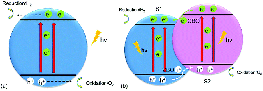 | ||
| Fig. 1 Schematic illustration of transfer of photogenerated charges in (a) a monolayered semiconductor and (b) a 2D vdW heterostructure of two monolayered semiconductors for water splitting. | ||
The most popular method to address the above obstacles is the formation of a type-II (staggered) van der Waals (vdW) heterostructure of two-dimensional (2D) materials,2 as shown in Fig. 2(b). The photogenerated electrons can be driven from the CB of semiconductor 2 (S2) to that of semiconductor 1 (S1), while the photoexcited holes will migrate from the VB of S1 to that of S2 under the assistance of the conduction-band offset (CBO) and valence-band offset (VBO), respectively,12 thus extending the lifetimes of the photogenerated charges and improving the efficiency of water splitting. The oxidation and reduction reactions which take place at the surface of S2 and S1, respectively, are helpful for separation of the photogenerated electrons and holes. Ever since graphene (G) unlocked the field of 2D materials because of its excellent properties,13–25 other 2D materials, such as transition-metal dichalcogenides (TMDs)26–28 and phosphorene,28–30 have also attracted wide attention. In particular, blue phosphorus (BlueP), a G-like material, has been a subject of investigations owing to its wide fundamental bandgap,31 stable honeycomb structure,32 high mobility,33,34 and novel thermal and thermomechanical characteristics.35 The magnetic and optical properties of BlueP have also been studied in first-principles calculations.36–38 An interesting revelation is that the Dirac cone can be built in BlueP by hydrogenation, halogenation,39 and four-fold-coordinated phosphorus atoms.40 The properties of BlueP can also be tuned by altering its structure,41,42 applying an electric field43 or strain,33,44 via doping,45–47 and by adsorption of certain species.48 All of these studies indicate that BlueP is a promising candidate for anode material,49 component of heterostructures,50,51 and for application in optoelectronics and nano-electronic devices.34 Furthermore, some works have demonstrated effective methods for the growth of BlueP.52–54 The 2D heterostructures formed by BlueP can not only preserve its outstanding properties, but also extend their application.7,55–57
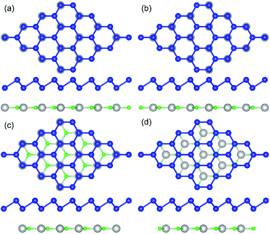 | ||
| Fig. 2 Top and side views of g-GaN/BlueP heterostructure with different stacking configurations: (a) H1-stacking; (b) H2-stacking; (c) H3-stacking; (d) H4-stacking. The blue, gray, and cyan spheres represent P, Ga, and N atoms, respectively. | ||
Graphene-like gallium nitride (g-GaN) is also considered to represent a new generation of 2D materials because of its remarkable properties.50,58 Studies show that g-GaN has a stable 2D structure and an indirect bandgap,59,60 and it can remain in high-temperature environments. The migration-enhanced encapsulated growth method can be used to prepare 2D g-GaN,61 whose properties can also be moderated by applying an external electric field or changing the stacking style.62 Moreover, g-GaN sheets and nanoribbons with Ga imperfections are considered promising candidates for application in spintronics.63 All of these investigations indicate that g-GaN is an excellent 2D material which has the potential to be used in photocatalytic, photovoltaic, and optical devices. There have been also some works on BlueP-based or g-GaN-based heterostructures,5,50,58 but there has been no attempt to elucidate band bending in a g-GaN/BlueP heterostructure. Since g-GaN and BlueP have the same hexagonal structure and a suitable lattice mismatch exists between the two materials, a heterostructure based on g-GaN and BlueP (g-GaN/BlueP) would be an ideal photocatalyst for water splitting, and it makes sense to pursue an investigation of said heterostructure. Considering that monolayered black phosphorene, a well-known phosphorene material, has been reported to exhibit remarkable optical properties when under strain, the effect of strain on the optical performance of a BlueP-based heterostructure was also investigated for comparison.64
This study focuses on the effects of band bending and strain on vdW heterostructures of 2D semiconductors for photocatalysis. The g-GaN/BlueP heterostructure was designed to act as a visible-light-driven photocatalyst for water splitting. The structures of 2D g-GaN, 2D BlueP, and the g-GaN/BlueP vdW heterostructure were optimized, and the most stable stacking configuration was obtained by first-principles calculation. Their band structures were then calculated to determine which band-energy structure of the g-GaN/BlueP vdW heterostructure has the ability to prevent recombination of photogenerated charges; the calculated band edge of the g-GaN/BlueP vdW heterostructure also explains its ability to induce the redox reaction of water splitting at a pH of 0. The band bending of the g-GaN/BlueP vdW heterostructure induced by a built-in electric field was then calculated and explained, and it was shown to be favorable for water splitting. The charge-difference analysis and potential drop across the interface of g-GaN/BlueP vdW heterostructure were carried out. Finally, the responses of the bandgap, energy, band edge, and light-absorption characteristics in the visible-light region of the g-GaN/BlueP vdW heterostructure to strain were investigated.
Computational methods
All calculations in our research were carried out using the first-principles method based on density functional theory (DFT).65–68 Using the Vienna Ab Initio Simulation Package (VASP), the exchange correlation functional was expressed by the Perdew–Burke–Ernzerhof (PBE) functional with generalized gradient approximation (GGA).69–73 To obtain more accurate bandgap values and results, the hybrid Heyd–Scuseria–Ernzerhof (HSE06) functional was also adopted.74–76 More specifically, the cut-off energy was set at 550 eV, and the atoms in the first Brillouin Zone (BZ) was conducted via 7 × 7 × 1 and 17 × 17 × 1 Monkhorst–Pack k-point grids for relaxation and static calculations, respectively. An energy of less than 1 × 10⁻⁵ eV was set as the convergence criterion, while 0.01 eV Å−1 was set for the residual force on each atom. The DFT-D2 method of Grimme64 (ref. 77) was considered for the van der Waals interactions in all simulations. A vacuum layer thickness of 20 Å was used to avoid interaction between adjacent atomic layers.The binding energy (Eb) of the heterostructure is defined as78–80
| Eb = Etotalg-GaN/BlueP−EtotalBlueP+g-GaN, | (1) |
| Δρ = ρg-GaN/BlueP − ρBlueP − ρg-GaN, | (2) |
 | (3) |
Results and discussion
The geometric structures of the two monolayered materials were first optimized via DFT, and the lattice constants of BlueP and g-GaN were calculated to be 3.275 and 3.255 Å, respectively; as reported in previous investigations, these values represent an acceptable lattice mismatch.50,58 An optimized lattice parameter of 3.265 Å was obtained for different stacking configurations of the heterostructure based on g-GaN and BlueP. When BlueP is placed on g-GaN, four high-symmetry structures can be obtained (Fig. 2), and they are referred to as H1, H2, H3, and H4 stacking. The binding energies were calculated to be 0.218, 0.128, 0.205, and 0.125 eV A−2 for H1, H2, H3, and H4 stacking, respectively, indicating that the heterostructures are formed by vdW forces.16,73 With the highest binding energy, H1 is the most stable stacking configuration, and the following discussions on the g-GaN/BlueP vdW heterostructure refer specifically to the structure with H1 stacking.The band structures of the two monolayers were calculated using the HSE06 functional (Fig. 3). The BlueP monolayer exhibits semiconducting characteristics, with an indirect bandgap of 2.768 eV. The VBM of BlueP is located between points K and Γ, while the CBM exists between points Γ and M. The inset in Fig. 3 shows the path of points K, M, and Γ in the first BZ. The g-GaN monolayer also possesses an indirect bandgap of 3.203 eV, and its CBM appears at point Γ whereas its VBM is located at point K. These results are all in good agreement with those in previous reports.7,50,58 Fig. 4(a) shows the staggered band structure of the g-GaN/BlueP vdW heterostructure obtained by HSE06 calculations; the black and red marks represent the contributions from BlueP and g-GaN, respectively. It can be seen that the g-GaN/BlueP vdW heterostructure is also a semiconductor with an indirect bandgap of 1.890 eV; the CBM and VBM of the heterostructure originate from BlueP and g-GaN, respectively. A break down of the charge density of the g-GaN/BlueP vdW heterostructure in Fig. 4(b) can further explain the contribution of P and N atoms to the CBM and VBM, respectively. The bandgap of the g-GaN/BlueP vdW heterostructure is larger than the required value of 1.23 eV, which indicates that it is a promising candidate for a photocatalyst in water splitting.
 | ||
| Fig. 3 Top and side views of (a) BlueP and (c) g-GaN. Band structures obtained by HSE06 of (b) BlueP and (d) g-GaN. The blue, gray, and cyan spheres represent P, Ga, and N atoms, respectively; the Fermi level is represented by the gray dashed line. | ||
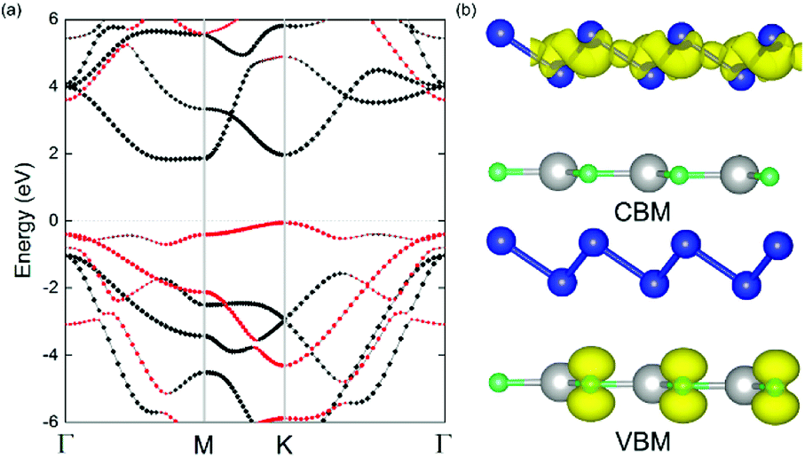 | ||
| Fig. 4 (a) Projected band structure of g-GaN/BlueP vdW heterostructure, obtained by HSE06 calculations. (b) Charge densities of CBM and VBM in g-GaN/BlueP vdW heterostructure; the Fermi level is represented by the gray dashed line; the blue, gray and cyan spheres represent P, Ga, and N atoms, respectively; the charge difference represented by the isosurface is set at 0.015 e Å−3. | ||
In addition to possessing the appropriate bandgap, the band edge of a photocatalyst for water splitting must also be at an appropriate position. Fig. 5 shows the band alignment of BlueP, g-GaN, and the g-GaN/BlueP vdW heterostructure with respect to the potentials of oxidation (O2/H2O) and reduction (H+/H2) for water splitting. As reported in an earlier study, the band edges of monolayered BlueP and monolayered g-GaN are suitable for water splitting.83 However, their respective bandgaps are too large (>2.20 eV), thus limiting the ability of the two monolayered materials for optical absorption. On the other hand, the band edge of the g-GaN/BlueP vdW heterostructure is closer than the band edges of monolayered BlueP and g-GaN to the potentials of oxidation and reduction, indicating that the heterostructure is a more efficient photocatalyst than the individual monolayers for water splitting.
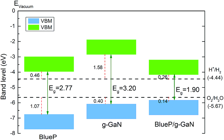 | ||
| Fig. 5 Band-edge alignment, obtained by HSE06, of BlueP monolayer, g-GaN monolayer, and g-GaN/BlueP vdW heterostructure. The potentials of oxidation (O2/H2O) and reduction (H+/H2) at pH = 0 for water splitting are also shown. | ||
When the g-GaN and BlueP monolayers are in contact with each other, electrons can migrate between the two materials because of the different work functions. The work function of a material is defined as Φ = Evac − EF, where Φ, Evac, and EF represent the work function, vacuum energy level, and Fermi level, respectively. Here, we use Φ1, Φ2, and Φ3 to represent the work functions of monolayered g-GaN, monolayered BlueP, and the g-GaN/BlueP vdW heterostructure, respectively. Because Φ2 is larger than Φ1, electrons will flow from g-GaN to BlueP until the Fermi levels and the vacuum levels of g-GaN (E1F and E1vac) and BlueP (E2F and E2vac) are aligned under equilibrium according to Anderson's rules,84,85 as shown in Fig. 6. With the electrons flowing from g-GaN to BlueP and owing to the electrostatic induction effect, the g-GaN layer is positively charged while the BlueP layer is negatively charged near the interface, which can induce a built-in electric field.86 Therefore, the electrons in the g-GaN layer are repelled by the negative charges in the BlueP layer, and the potential energy rises, resulting in the g-GaN band bending upward near the interface; for the same reason, the BlueP band near the interface bends downward.86–88 The region of band bending induced by the built-in electric field is called the space-charge layer.10 The calculated CB energy of pristine BlueP is −3.975 eV, and it becomes more negative and reaches −4.180 eV in the heterostructure; the VB energy of g-GaN changes from −6.066 to −5.814 eV after it makes contact with BlueP, which can further explain the band bending in the g-GaN/BlueP vdW heterostructure.
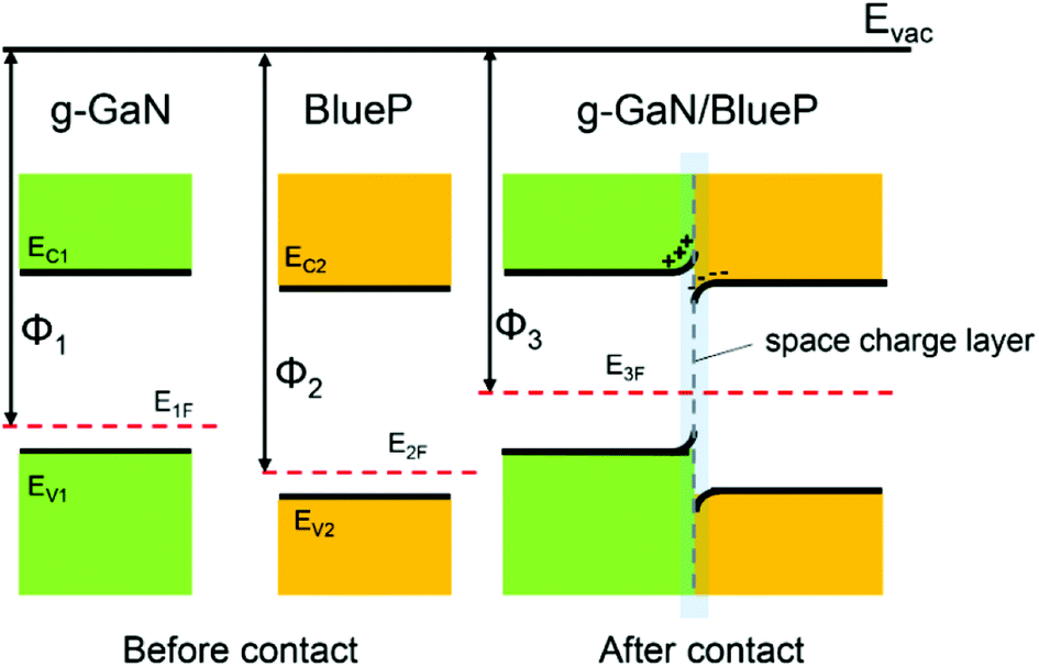 | ||
| Fig. 6 Energy-band diagrams of BlueP and g-GaN; schematic diagram of vdW heterostructure of BlueP and g-GaN. | ||
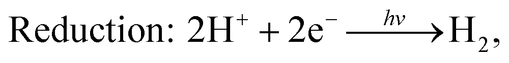
As discussed earlier, the g-GaN/BlueP vdW heterostructure shown in Fig. 1(b) can sufficiently extend the lifetime of photoexcited charges when it is used as a photocatalyst for water splitting. After absorbing the energy of incident photons, the photoexcited electrons will migrate from the VB of g-GaN and BlueP to their CB, leaving holes in the VB. With the assistance of the CBO and VBO, the electrons can move from the CB of g-GaN to that of BlueP, while the holes are constantly driven from the VB of BlueP to that of g-GaN.89,90 Some reports also claim that the photogenerated electrons and holes can directly recombine from the VB to the CB of the heterostructure, thus reducing the accumulation of charges and improving the efficiency of photocatalysis with or without electron shuttles, i.e. the Z-scheme of the water-splitting system.4,6,9,11,88,91–94 In general, the built-in electric field plays a vital role to separate the photogenerated charges. Oxidation and reduction of water on the surface of the g-GaN/BlueP vdW heterostructure can be represented by the following reactions:95


The charge difference in the g-GaN/BlueP vdW heterostructure was calculated using Bader charge-population analysis.14,96–98 As shown in Fig. 7(a), the Ga atoms always act as a donor of electrons, and the charge transferred from the g-GaN layer to the BlueP layer is 0.0197 |e|, which causes a potential drop across the interface of the g-GaN/BlueP vdW heterostructure. In Fig. 7(b), the drop in electrostatic potential from the BlueP layer to the g-GaN layer is 7.754 eV, which favors the separation of photogenerated charges. In addition, even though the g-GaN/BlueP vdW heterostructure has aligned Fermi levels, the g-GaN and BlueP layers retain their own electron affinities and work functions, which means that there are slight variations in the vacuum energy level across the interface of the g-GaN/BlueP vdW heterostructure. As shown in the inset of Fig. 7(b), the electron affinity of the BlueP layer is stronger than that in the g-GaN layer of the heterostructure, and the vacuum energy level slightly declines from the BlueP layer towards the g-GaN layer. Because the BlueP layer and g-GaN layer contribute to the CBM, VBM, and vacuum energy level of the heterostructure, the band energy of the g-GaN/BlueP vdW heterostructure can be obtained from the CBM and VBM by comparing the vacuum energy levels of the individual BlueP and g-GaN layers. To focus on the band bending of the g-GaN/BlueP vdW heterostructure under equilibrium, the small change in vacuum energy level across the interface is not shown in Fig. 6(a).
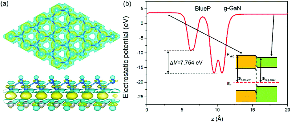 | ||
| Fig. 7 (a) Isosurface with charge difference of 0.0004 e Å−3. (b) Potential drop across the interface of the g-GaN/BlueP vdW heterostructure. The yellow and cyan regions represent the gaining and losing, respectively, of electrons; the blue, gray, and cyan spheres represent P, Ga, and N atoms, respectively. | ||
In this study, we also utilized strain to tune the electronic structure and optical-absorption performance of the g-GaN/BlueP vdW heterostructure. As shown in Fig. 8(a), the band level of the VBM slowly increases as the strain changes from 5% compressive stress to 10% tensile stress, while the CBM increases to the peak value at 1% compressive stress and decreases with increasing tensile strain. When the redox potentials of water splitting at a pH of 0 are compared with the band alignment of the g-GaN/BlueP vdW heterostructure, it can be seen that the heterostructure is still a promising photocatalyst for water splitting at strains from −4% to 3% (positive values represent tensile strain, and negative ones represent compressive strain). As shown by the strain-induced changes in energy of the g-GaN/BlueP vdW heterostructure (Fig. 7(b)), the heterostructure has the lowest energy when there is no strain, and the energy quickly increases under tensile or compressive stress. On the other hand, the bandgap sharply increases with decreasing compressive strain (down to 1%). The bandgap then quickly drops, indicating that an excessively high tensile strain is not favorable for water splitting by the g-GaN/BlueP vdW heterostructure. The extremely narrow bandgap induced by a large tensile strain may not be appropriate for the right band edge, while a wide bandgap may limit the ability of the heterostructure to absorb light. Therefore, it is necessary to study the response of the optical-absorption ability of g-the GaN/BlueP vdW heterostructure to variations in strain.
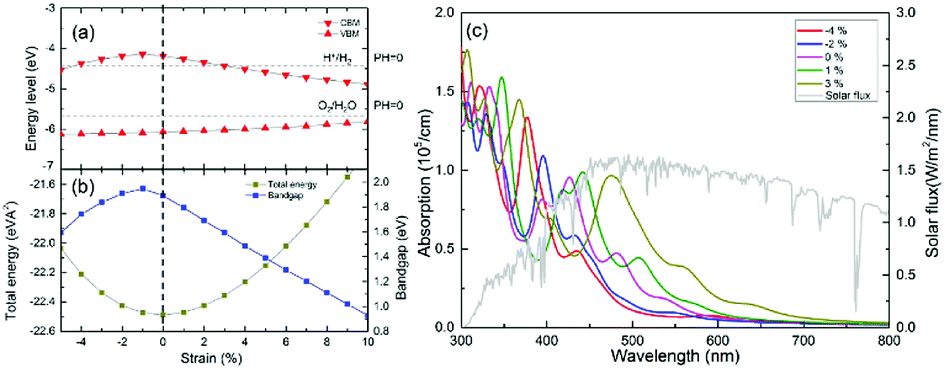 | ||
| Fig. 8 Effect of strain, calculated by HSE06 functional, on (a) band-edge position, (b) bandgap, and (c) optical absorption of g-GaN/BlueP vdW heterostructure. The redox potential at pH of 0 for water splitting is represented by the cyan dotted line. | ||
Light absorption by the g-GaN/BlueP vdW heterostructure was calculated in the wavelength range of visible light, and the results are shown in Fig. 8(c). The peak values of absorption for the g-GaN/BlueP vdW heterostructure with strain of −4%, −2%, 0%, 1%, and 3% are 5.26 × 10⁵, 4.33 × 10⁵, 3.80 × 10⁵, 0.98 × 10⁵, and 0.96 × 105 cm, respectively, and they take place at wavelengths of 377.362, 396.406, 427.286, 442.135, and 474.136 nm. These results reveal that the g-GaN/BlueP vdW heterostructure has excellent ability for absorption of visible light. As the applied strain is changed from 3% to −4%, the performance in optical absorption slowly improves. When the g-GaN/BlueP vdW heterostructure is subjected to compressive strain, the best optical absorption performance is observed far from the visible-light region, which also agrees with the effect of a wide bandgap on the light-absorption ability. Therefore, the g-GaN/BlueP vdW heterostructure can be considered as a reasonable and ideal visible-light-driven photocatalyst for water splitting, and it can even be used in photocatalytic, photovoltaic, and optical devices.
In addition to simple bilayers of dissimilar 2D materials, multilayered structures can also be prepared as van der Waals heterostructures. Therefore, the number of layers is another important factor of the optical properties. For example, it has been reported that a multilayered structure can exhibit better performance in the absorption of visible light.99
Conclusions
The structures of monolayered g-GaN and BlueP were optimized by DFT, and a g-GaN/BlueP heterostructure can be formed by vdW interaction. The most stable structure of the g-GaN/BlueP vdW heterostructure was obtained from four stacking configurations. At the same time, the band structure calculated by the HSE06 functional reveals that the heterostructure is a semiconductor with a bandgap of 1.890 eV, and the CBM and VBM are contributed by BlueP and g-GaN, respectively. Compared with the redox potentials at a pH of 0, the calculated energy of the band edge of the g-GaN/BlueP vdW heterostructure shows that it is a better photocatalyst than monolayered g-GaN and monolayered BlueP for water spitting. The generation of a built-in electric field in the g-GaN/BlueP vdW heterostructure and how it induces the band bending were demonstrated, which further illustrate the operating principle of the heterostructure as a photocatalyst for water splitting. The band-bending characteristic is also demonstrated by first-principles calculations. The charge difference given by Bader charge-population analysis shows that the g-GaN layer donates 0.0197 |e| to the BlueP layer when the g-GaN/BlueP vdW heterostructure is in equilibrium, which causes a potential drop of 7.754 eV. Furthermore, the evolution of the band edge, bandgap, and total energy of the g-GaN/BlueP vdW heterostructure with strain shows that the bandgap of the heterostructure increases under compressive strain, but it drops with tensile strain, and the heterostructure maintains its ability to split water at a strain of −4% to 3%. The g-GaN/BlueP vdW heterostructure under strain in this range also shows the ability for optical absorption in the visible-light region. All these results reveal that the g-GaN/BlueP vdW heterostructure is a promising candidate for a water-splitting photocatalyst in the visible-light range.Conflicts of interest
There are no conflicts to declare.Acknowledgements
This investigation was funded by the Transformation project of Scientific and Technological Achievements of JiangSu (grant number BA2015077), National Natural Science Foundation of China (grant number 51675100), National Science and Technology Major Projects of Numerical control equipment (grant number 2016ZX04004008), the Innovation Project Foundation of Southeast University (grant number 3202008708).Notes and references
- Y. Qu and X. Duan, Chem. Soc. Rev., 2013, 42, 2568–2580 RSC.
- S. Wang, C. Ren, H. Tian, J. Yu and M. Sun, Phys. Chem. Chem. Phys., 2018, 20, 13394–13399 RSC.
- Z. Guan, C.-S. Lian, S. Hu, S. Ni, J. Li and W. Duan, J. Phys. Chem. C, 2017, 121, 3654–3660 CrossRef CAS.
- Z.-F. Huang, J. Song, X. Wang, L. Pan, K. Li, X. Zhang, L. Wang and J.-J. Zou, Nano Energy, 2017, 40, 308–316 CrossRef CAS.
- B.-J. Wang, X.-H. Li, R. Zhao, X.-L. Cai, W.-Y. Yu, W.-B. Li, Z.-S. Liu, L.-W. Zhang and S.-H. Ke, J. Mater. Chem. A, 2018, 6, 8923–8929 RSC.
- A. Kudo and Y. Miseki, Chem. Soc. Rev., 2009, 38, 253–278 RSC.
- B.-J. Wang, X.-H. Li, X.-L. Cai, W.-Y. Yu, L.-W. Zhang, R.-Q. Zhao and S.-H. Ke, J. Phys. Chem. C, 2018, 122, 7075–7080 CrossRef CAS.
- H. L. Zhuang and R. G. Hennig, Chem. Mater., 2013, 25, 3232–3238 CrossRef CAS.
- H. Wang, L. Zhang, Z. Chen, J. Hu, S. Li, Z. Wang, J. Liu and X. Wang, Chem. Soc. Rev., 2014, 43, 5234–5244 RSC.
- A. G. Tamirat, J. Rick, A. A. Dubale, W.-N. Su and B.-J. Hwang, Nanoscale Horiz., 2016, 1, 243–267 RSC.
- X. Chen, S. Shen, L. Guo and S. S. Mao, Chem. Rev., 2010, 110, 6503–6570 CrossRef CAS PubMed.
- S. Wang, H. Tian, C. Ren, J. Yu and M. Sun, Sci. Rep., 2018, 8, 12009 CrossRef PubMed.
- M. Sun, Q. Ren, Y. Zhao, J.-P. Chou, J. Yu and W. Tang, Carbon, 2017, 120, 265–273 CrossRef CAS.
- M. Sun, W. Tang, Q. Ren, S. Wang, J. Yu, Y. Du and Y. Zhang, Appl. Surf. Sci., 2015, 356, 668–673 CrossRef CAS.
- A. K. Geim and K. S. Novoselov, in Nanoscience and Technology, 2010, pp. 11–19 Search PubMed.
- X. Chen, F. Tian, C. Persson, W. Duan and N. X. Chen, Sci. Rep., 2013, 3, 3046 CrossRef PubMed.
- X. Chen, Y. Liu, B.-L. Gu, W. Duan and F. Liu, Phys. Rev. B: Condens. Matter Mater. Phys., 2014, 90(12), 121403 CrossRef.
- D.-H. Kim, M.-S. Kim and H.-D. Kim, Appl. Surf. Sci., 2015, 359, 55–60 CrossRef CAS.
- M. Rafique, Y. Shuai, H.-P. Tan and M. Hassan, Appl. Surf. Sci., 2017, 399, 20–31 CrossRef CAS.
- M. Rafique, Y. Shuai, H.-P. Tan and H. Muhammad, Appl. Surf. Sci., 2017, 408, 21–33 CrossRef CAS.
- S. Seifoori and H. Hajabdollahi, Appl. Surf. Sci., 2015, 351, 565–572 CrossRef CAS.
- Y. Wang, Q. Yang, C. Zhong and J. Li, Appl. Surf. Sci., 2017, 407, 532–539 CrossRef CAS.
- E. Zaminpayma, M. E. Razavi and P. Nayebi, Appl. Surf. Sci., 2017, 414, 101–106 CrossRef CAS.
- T. Zhang, H. Sun, F. Wang, W. Zhang, S. Tang, J. Ma, H. Gong and J. Zhang, Appl. Surf. Sci., 2017, 425, 340–350 CrossRef CAS.
- W. Yang, Z. Gao, X. Ding, G. Lv and W. Yan, Appl. Surf. Sci., 2018, 455, 940–951 CrossRef CAS.
- M. M. Dong, C. He and W. X. Zhang, J. Phys. Chem. C, 2017, 121, 22040–22048 CrossRef CAS.
- K. D. Pham, N. N. Hieu, H. V. Phuc, B. D. Hoi, V. V. Ilysov, B. Amin and C. V. Nguyen, Comput. Mater. Sci., 2018, 153, 438–444 CrossRef CAS.
- B. You, X. Wang, Z. Zheng and W. Mi, Phys. Chem. Chem. Phys., 2016, 18, 7381–7388 RSC.
- H. V. Phuc, V. V. Ilyasov, N. N. Hieu and C. V. Nguyen, Vacuum, 2018, 149, 231–237 CrossRef CAS.
- L. Li, Y. Yu, G. J. Ye, Q. Ge, X. Ou, H. Wu, D. Feng, X. H. Chen and Y. Zhang, Nat. Nanotechnol., 2014, 9, 372–377 CrossRef CAS PubMed.
- Z. Zhu and D. Tomanek, Phys. Rev. Lett., 2014, 112, 176802 CrossRef.
- M. Sun, W. Tang, Q. Ren, S.-k. Wang, J. Yu and Y. Du, Appl. Surf. Sci., 2015, 356, 110–114 CrossRef CAS.
- L. Z. Liu, X. L. Wu, X. X. Liu and P. K. Chu, Appl. Surf. Sci., 2015, 356, 626–630 CrossRef CAS.
- J. Xiao, M. Long, C.-S. Deng, J. He, L.-L. Cui and H. Xu, J. Phys. Chem. C, 2016, 120, 4638–4646 CrossRef CAS.
- H. Sun, G. Liu, Q. Li and X. G. Wan, Phys. Lett. A, 2016, 380, 2098–2104 CrossRef CAS.
- Y. Ding and Y. Wang, J. Phys. Chem. C, 2015, 119, 10610–10622 CrossRef CAS.
- Y. Mogulkoc, M. Modarresi, A. Mogulkoc and Y. O. Ciftci, Comput. Mater. Sci., 2016, 124, 23–29 CrossRef CAS.
- D. A. Ospina, C. A. Duque, M. E. Mora-Ramos and J. D. Correa, Comput. Mater. Sci., 2017, 135, 43–53 CrossRef CAS.
- M. Sun, S. Wang, J. Yu and W. Tang, Appl. Surf. Sci., 2017, 392, 46–50 CrossRef CAS.
- Y. Li and X. Chen, 2D Materials, 2014, 1, 031002 CrossRef.
- R. Li, Y. Tao, Z.-l. Liu and Y. Tan, Phys. E, 2017, 88, 174–181 CrossRef CAS.
- P.-Y. Xiong, S.-Z. Chen, W.-X. Zhou and K.-Q. Chen, Phys. Lett. A, 2017, 381, 2016–2020 CrossRef CAS.
- B. Ghosh, S. Nahas, S. Bhowmick and A. Agarwal, Phys. Rev. B: Condens. Matter Mater. Phys., 2015, 91(11), 115433 CrossRef.
- G. Yang, Z. Xu, Z. Liu, S. Jin, H. Zhang and Z. Ding, J. Phys. Chem. C, 2017, 121, 12945–12952 CrossRef CAS.
- M. Sun, Y. Hao, Q. Ren, Y. Zhao, Y. Du and W. Tang, Solid State Commun., 2016, 242, 36–40 CrossRef CAS.
- F. Safari, M. Fathipour and A. Yazdanpanah Goharrizi, J. Comput. Electron., 2018, 17, 499–513 CrossRef CAS.
- W. X. Zhang, J. W. Zhao, W. H. He, L. J. Luan and C. He, Chem. Phys. Lett., 2017, 675, 20–26 CrossRef CAS.
- F. Safari, M. Moradinasab, M. Fathipour and H. Kosina, Appl. Surf. Sci., 2019, 464, 153–161 CrossRef CAS.
- Q.-F. Li, C.-G. Duan, X. G. Wan and J.-L. Kuo, J. Phys. Chem. C, 2015, 119, 8662–8670 CrossRef CAS.
- M. Sun, J. P. Chou, J. Yu and W. Tang, Phys. Chem. Chem. Phys., 2017, 19, 17324–17330 RSC.
- J. Guo, Z. Zhou, T. Wang, Z. Lu, Z. Yang and C. Liu, Curr. Appl. Phys., 2017, 17, 1714–1720 CrossRef.
- C. Gu, S. Zhao, J. L. Zhang, S. Sun, K. Yuan, Z. Hu, C. Han, Z. Ma, L. Wang, F. Huo, W. Huang, Z. Li and W. Chen, ACS Nano, 2017, 11, 4943–4949 CrossRef CAS PubMed.
- J. L. Zhang, S. Zhao, C. Han, Z. Wang, S. Zhong, S. Sun, R. Guo, X. Zhou, C. D. Gu, K. D. Yuan, Z. Li and W. Chen, Nano Lett., 2016, 16, 4903–4908 CrossRef CAS PubMed.
- N. Han, N. Gao and J. Zhao, J. Phys. Chem. C, 2017, 121, 17893–17899 CrossRef CAS.
- Z. Guo, N. Miao, J. Zhou, B. Sa and Z. Sun, J. Mater. Chem. C, 2017, 5, 978–984 RSC.
- T. Kaewmaraya, P. Srepusharawoot, T. Hussian and V. Amornkitbamrung, ChemPhysChem, 2018, 19, 612–618 CrossRef CAS PubMed.
- Y. Mogulkoc, M. Modarresi, A. Mogulkoc and B. Alkan, Phys. Chem. Chem. Phys., 2018, 20, 12053–12060 RSC.
- M. Sun, J.-P. Chou, Q. Ren, Y. Zhao, J. Yu and W. Tang, Appl. Phys. Lett., 2017, 110, 173105 CrossRef.
- A. Onen, D. Kecik, E. Durgun and S. Ciraci, Phys. Rev. B, 2016, 93(8), 085431 CrossRef.
- H. Şahin, S. Cahangirov, M. Topsakal, E. Bekaroglu, E. Akturk, R. T. Senger and S. Ciraci, Phys. Rev. B: Condens. Matter Mater. Phys., 2009, 80(15), 155453 CrossRef.
- Z. Y. Al Balushi, K. Wang, R. K. Ghosh, R. A. Vila, S. M. Eichfeld, J. D. Caldwell, X. Qin, Y. C. Lin, P. A. DeSario, G. Stone, S. Subramanian, D. F. Paul, R. M. Wallace, S. Datta, J. M. Redwing and J. A. Robinson, Nat. Mater., 2016, 15, 1166–1171 CrossRef CAS PubMed.
- D. Xu, H. He, R. Pandey and S. P. Karna, J. Phys. Condens. Matter, 2013, 25, 345302 CrossRef PubMed.
- H. Li, J. Dai, J. Li, S. Zhang, J. Zhou, L. Zhang, W. Chu, D. Chen, H. Zhao and J. Yang, J. Phys. Chem. C, 2010, 114, 11390–11394 CrossRef CAS.
- B. Sa, Y.-L. Li, J. Qi, R. Ahuja and Z. Sun, J. Phys. Chem. C, 2014, 118, 26560–26568 CrossRef CAS.
- Y. Cai, Z. Bai, H. Pan, Y. P. Feng, B. I. Yakobson and Y. W. Zhang, Nanoscale, 2014, 6, 1691–1697 RSC.
- G. Guan, S. Zhang, S. Liu, Y. Cai, M. Low, C. P. Teng, I. Y. Phang, Y. Cheng, K. L. Duei, B. M. Srinivasan, Y. Zheng, Y. W. Zhang and M. Y. Han, J. Am. Chem. Soc., 2015, 137, 6152–6155 CrossRef CAS PubMed.
- Z. G. Yu, Y. Cai and Y. W. Zhang, Sci. Rep., 2015, 5, 13783 CrossRef PubMed.
- T. P. Kaloni, L. Kou, T. Frauenheim and U. Schwingenschlögl, Appl. Phys. Lett., 2014, 105, 233112 CrossRef.
- Y. Cai, G. Zhang and Y. W. Zhang, J. Am. Chem. Soc., 2014, 136, 6269–6275 CrossRef CAS PubMed.
- Y. Cai, H. Zhou, G. Zhang and Y.-W. Zhang, Chem. Mater., 2016, 28, 8611–8621 CrossRef CAS.
- N. Feng, W. Mi, Y. Cheng, Z. Guo, U. Schwingenschlogl and H. Bai, ACS Appl. Mater. Interfaces, 2014, 6, 4587–4594 CrossRef CAS PubMed.
- N. Huo, Z. Wei, X. Meng, J. Kang, F. Wu, S.-S. Li, S.-H. Wei and J. Li, J. Mater. Chem. C, 2015, 3, 5467–5473 RSC.
- M. Sun, J. P. Chou, Y. Zhao, J. Yu and W. Tang, Phys. Chem. Chem. Phys., 2017, 19, 28127–28132 RSC.
- D. Keçik, C. Bacaksiz, R. T. Senger and E. Durgun, Phys. Rev. B: Condens. Matter Mater. Phys., 2015, 92, 165408 CrossRef.
- J. Kang, S. Tongay, J. Zhou, J. Li and J. Wu, Appl. Phys. Lett., 2013, 102, 012111 CrossRef.
- W. Hu, T. Wang, R. Zhang and J. Yang, J. Mater. Chem. C, 2016, 4, 1776–1781 RSC.
- S. Grimme, J. Comput. Chem., 2006, 27, 1787–1799 CrossRef CAS PubMed.
- J. Liao, B. Sa, J. Zhou, R. Ahuja and Z. Sun, J. Phys. Chem. C, 2014, 118, 17594–17599 CrossRef CAS.
- Q. Peng, Z. Wang, B. Sa, B. Wu and Z. Sun, Sci. Rep., 2016, 6, 31994 CrossRef CAS.
- Q. Peng, Z. Wang, B. Sa, B. Wu and Z. Sun, ACS Appl. Mater. Interfaces, 2016, 8, 13449–13457 CrossRef CAS PubMed.
- M. Sun, J.-P. Chou, L. Shi, J. Gao, A. Hu, W. Tang and G. Zhang, ACS Omega, 2018, 3, 5971–5979 CrossRef CAS.
- M. Sun, J.-P. Chou, J. Gao, Y. Cheng, A. Hu, W. Tang and G. Zhang, ACS Omega, 2018, 3, 8514–8520 CrossRef CAS.
- Q. Yang, C.-J. Tan, R.-S. Meng, J.-K. Jiang, Q.-H. Liang, X. Sun, D.-G. Yang and X.-P. Chen, IEEE Electron Device Lett., 2017, 38, 145–148 CAS.
- V. E. Borisenko and S. Ossicini, What is what in the Nanoworld: A Handbook on Nanoscience and Nanotechnology, John Wiley & Sons, 2013 Search PubMed.
- Y. Gao, Y. Jing, J. Liu, X. Li and Q. Meng, Appl. Therm. Eng., 2017, 113, 1419–1425 CrossRef CAS.
- Z. Zhang and J. T. Yates Jr, Chem. Rev., 2012, 112, 5520–5551 CrossRef CAS.
- S. Bai, X. Li, Q. Kong, R. Long, C. Wang, J. Jiang and Y. Xiong, Adv. Mater., 2015, 27, 3444–3452 CrossRef CAS PubMed.
- L. J. Zhang, S. Li, B. K. Liu, D. J. Wang and T. F. Xie, ACS Catal., 2014, 4, 3724–3729 CrossRef CAS.
- L. Xu, W.-Q. Huang, L.-L. Wang, Z.-A. Tian, W. Hu, Y. Ma, X. Wang, A. Pan and G.-F. Huang, Chem. Mater., 2015, 27, 1612–1621 CrossRef CAS.
- Q. Qiao, K. Yang, L.-L. Ma, W.-Q. Huang, B.-X. Zhou, A. Pan, W. Hu, X. Fan and G.-F. Huang, J. Phys. D: Appl. Phys., 2018 Search PubMed.
- M. Ni, M. K. H. Leung, D. Y. C. Leung and K. Sumathy, Renewable Sustainable Energy Rev., 2007, 11, 401–425 CrossRef CAS.
- S. Chen, Y. Qi, T. Hisatomi, Q. Ding, T. Asai, Z. Li, S. S. Ma, F. Zhang, K. Domen and C. Li, Angew. Chem., 2015, 54, 8498–8501 CrossRef CAS PubMed.
- X. Wang, G. Liu, Z. G. Chen, F. Li, L. Wang, G. Q. Lu and H. M. Cheng, Chem. Commun., 2009, 3452–3454 RSC.
- J. Yan, H. Wu, H. Chen, Y. Zhang, F. Zhang and S. F. Liu, Appl. Catal., B, 2016, 191, 130–137 CrossRef CAS.
- J. S. Jang, H. G. Kim and J. S. Lee, Catal. Today, 2012, 185, 270–277 CrossRef CAS.
- G. Henkelman, A. Arnaldsson and H. Jónsson, Comput. Mater. Sci., 2006, 36, 354–360 CrossRef.
- E. Sanville, S. D. Kenny, R. Smith and G. Henkelman, J. Comput. Chem., 2007, 28, 899–908 CrossRef CAS PubMed.
- W. Tang, E. Sanville and G. Henkelman, J. Phys. Condens. Matter, 2009, 21, 084204 CrossRef CAS PubMed.
- L. Xu, W.-Q. Huang, W. Hu, K. Yang, B.-X. Zhou, A. Pan and G.-F. Huang, Chem. Mater., 2017, 29, 5504–5512 CrossRef CAS.
| This journal is © The Royal Society of Chemistry 2019 |