DOI:
10.1039/C8RA09370A
(Paper)
RSC Adv., 2019,
9, 2180-2188
Non-monotonous size-dependent photoluminescence and excitonic relaxations in nanostructured ZnO thin films†
Received
13th November 2018
, Accepted 29th December 2018
First published on 17th January 2019
Abstract
The size dependence of room-temperature photoluminescence (PL) accompanied with near-band-edge emission (NBE) and defect-associated green emission (GE) was investigated using high-quality crystalline nanostructured ZnO thin films with grain sizes varying from 29 nm to 2 nm. The size dependence of correlated intensities of the PL bands was pursued in correlation with structural and defect evolution revealed by X-ray photoelectron spectroscopy (XPS) and previous studies of XRD and Raman scattering. In contrast to the influence of thermally activated reconstruction and changes in defect densities, quantum size effects emerging at grain sizes below a critical value, i.e., dc ∼ 10 nm were inspected in relation to the observed blueshift in the bandgap and correlated variations in the size dependence of the intensity of NBE and GE. Taking into account the geometry-modelled relative emission efficiency, (i) the observed overall linear size dependence of the relative intensity INBE/IGE was consistent with assuming a 1.05 nm-thick GE-active surface layer, and (ii) a local maximum of INBE/IGE emerging near grain radius R ≈ 4 nm was identified in relation to the theoretically predicted local minimum in size-dependent exciton radiative lifetime due to the intrinsic quantum nature of excitons confined in ZnO. Our results have provided new insights into non-monotonous size-dependent PL of ZnO, which can benefit future photoelectronic device design by taking advantage of the size-controlled stability of confined excitons in nanostructured thin films and luminescent quantum dots.
1. Introduction
Due to the existence of highly stable and tunable excitons (binding energy, 60 meV) in wurtzite zinc oxide (ZnO), its powder as well as various forms of nanostructures exhibits strong excitonic emission even at elevated temperatures.1–4 The above property of ZnO facilitates its use in versatile optoelectronic applications, e.g., in light-emitting diodes and lasing devices with improved performance.5 At the nanoscale, when the crystal size is reduced to approach the wavelengths of electronic wave functions, quantum effects due to spatially confined carrier states are expected to result in extraordinary properties such as a dramatic change in band structure.6,7 The critical size for such quantum confinement effects required to dominate the optoelectronic properties is measured with the bulk exciton Bohr radius, i.e., aB = 2.34 nm.2 ZnO nanostructures with a radius (R) in regions8 of the strong (R < 2aB)9–13 and weak (R > 2aB) confinement10–15 have been experimentally investigated. For instance, the third-order nonlinear susceptibility of ZnO nanoparticles (NPs) with an average size of 3.7 nm was found to be ∼500 times larger than that of the bulk counterpart, which was attributed to exciton confinement and optical Stark effects.16
Size-dependent photoluminescence (PL) spectroscopy has provided convenient access to study the confinement-induced perturbations in the electronic system. Systematic blueshifts in the exciton emission with decreasing particle size were considered to signify quantum confinement effects in the embedded nanoscale heterostructures17 and isolated quantum dots (QDs) in various forms.11–14,18–21 Recently, the elongated radiative exciton lifetime for ZnO QDs having sizes in the range from 3.7 to 6.2 nm has been reported and is attributed to acceptor-bound excitons located within a near-surface region,11 which also controls the exciton emission of ZnO QDs having sizes from 2 to 6 nm.22 The above findings revealed the enhanced exciton stability in the investigated smallest QDs.11 However, the theoretically22 estimated lifetime of an acceptor-bound exciton is two orders of magnitude larger than the experimentally measured value.11 Moreover, the calculated lifetime of an ionized acceptor–exciton complex decreases with decreasing QD size,22 which is contradictory to the size dependence in the observed exciton lifetime.11 The existence of a dark exciton state was proposed to account for the very long luminescence lifetime of ∼0.1 μs for ZnO nanocrystals with an average size of ∼3 nm.23 On the contrary, theoretical calculations disproved the possibility of a dark exciton ground state forming in ZnO QDs.24 In addition to the intrinsic radiative decay being controlled by oscillator strength,22,25 for a full understanding of exciton emission, we have to consider the relaxation channels due to competing radiative and defect-related nonradiative decays. Recently, it has been shown that the defect state dominates the quantum efficiencies of photoexcited luminescence in ZnO powders.26 For instance, in ZnO films with grain diameters varying from 2500 nm down to 40 nm, both the intensity and decay time of PL were found to follow correlated relations dominated by nonradiative exciton decay via surface and/or interface states in the grain boundaries.27 The grain is defined as a volume inside crystalline materials with a specific crystallographic orientation. As compared with the observations for the bulk counterpart, strongly reduced lifetimes from 6 ps to 22 ps (ref. 14) and ∼50 ps (ref. 12) have been reported for exciton emission from ZnO nanocrystals. The lifetime reduction was proposed to be due to nonradiative recombination via surface states, which may dramatically accelerate the recombination processes with decreasing nanocrystal size.28,29 In fact, experimentally observed and presumably defect-dominated nonradiative exciton lifetimes12,14 lie within the lifetime range that is theoretically determined for the exciton ground state confined in ZnO QDs (2 nm to 6 nm).22,25 Furthermore, the size-dependence of relative PL intensities has been modelled and ascribed to geometrical effects and size-correlated density variations of luminescent defect states in ZnO nanowires.30,31 In view of the unambiguous identification of emission peculiarities occurring due to confined excitons, it is important to clarify the contributions to the exciton recombination via nonradiative defect states, which is challenging and can be related to discrepancies between the discussed experimental11,23 and theoretical22,24 studies.
In this study, instead of solution-based methods that are mostly adopted for preparing small-sized crystals,11,23 vapour-phase sputtering deposition was utilized for fabricating ZnO to suppress the uncontrolled contaminations and defects. Post-deposition annealing at various temperatures resulted in high-quality crystalline nanostructured ZnO thin films with grain sizes varying from 29 nm to 2 nm,32 allowing the investigation of size-dominated properties for crystal dimensions down to the regime of strong confinement. Size-dependent PL consisting of ultraviolet near-band-edge emission (NBE) of excitonic emission and visible green deep-level emission (DLE) associated with near-surface defect states29 was pursued in correlation with structural and defect evolution revealed by X-ray photoelectron spectroscopy (XPS) and previous studies of XRD and Raman scattering.32 Peculiar intensity variations found in the size dependence of NBE and DLE indicated a critical size dc ∼ 10 nm for observing quantum confinement effects in PL. This is consistent with the critical size for observing the weakening of electron-phonon coupling (EPC) in small ZnO grains, which has been previously revealed by Raman scattering and is related to reduced Fröhlich interactions due to the less polar nature observed from XRD.32 In contrast to the influences of annealing-induced reconstruction and changes in defect densities, the intrinsic quantum size effects were inspected in terms of observed size-dependent intensity of NBE and DLE taking into account the theoretical predictions on excitonic lifetime and modelled size dependence of the relative emission intensity. A possible extension of the validity range of a volume-weighting (VW) model33 to the intermediate confined regime will be discussed by taking into account the theoretically proposed dead layer for confined excitons.
2. Experimental
A detailed structural and morphological analysis of granular ZnO films (prepared by vapour-phase sputtering deposition followed by thermal annealing at temperatures TA in an ambient atmosphere) carried out using X-ray diffraction (XRD) and scanning electron microscopy (SEM) is given in our previous work.32 Post-deposition thermal annealing leads to the transformation of nanoplate-like morphology to the well inter-connected sphere-like granular films, as can be seen from SEM images along with the mean diameter 〈d〉 in Fig. 1(a). Preferential growth along the c-axis was revealed with the dominating (002) reflection, whereas other weak diffraction peaks of ZnO suggested the presence of some randomly oriented grains, as can be seen from the XRD spectra in Fig. 1(b). The solid line represents the “F(calc) weighted” LaBail extraction analysis for the XRD pattern (crosses) and fitting parameters are summarized in the ESI in Table S1.† The calculated grain size d(101) of as-prepared (RT) ZnO film and those of the ZnO films annealed at 100 °C, 200 °C, 300 °C, 400 °C, 500 °C, 600 °C, 700 °C and 800 °C for a duration of 1 h using the Scherrer's formula are 2 nm, 5 nm, 7 nm, 8 nm, 10 nm, 16 nm, 26 nm, 24 nm, and 29 nm, respectively. Fig. 1(c) and (d) show the d(101) dependence of fitted values of c/a and the internal parameter u, revealing the low polar nature of small-sized granular films, and the details can be found in our previous work.32 The EPC strength deduced from the ratio of the second- to the first-order Raman scattering intensity showed a linear decreasing behavior with the decrease in grain size down to 10 nm, which in principle resulted from the Fröhlich interaction. However, below a critical size of 9(1) nm, a slight depression with minimum EPC strength around ∼0.55 was obtained. Based on structural properties and Raman scattering, we have suggested that in the quantum confined spatial system, the low polar nature in granular ZnO films leads to weak EPC strength. To study the effect of quantum confinement on the band gap and trap levels, the luminescence properties of granular ZnO films having various sizes were investigated at room temperature with a Jobin Yvon T64000 spectrometer (Horiba Scientific, Paris, France) using a continuous-wave laser of 325 nm for excitation. The PL spectra were detected from 250 nm to 800 nm by a QE65000 charge-coupled device imaging spectrometer. Photoelectron spectroscopy (XPS) was performed by a Thermo K-Alpha spectrometer X-ray using the Al Kα line from a micro focus monochromatic X-ray source. Deconvolution of XPS and PL spectra was carried out using Fityk 0.9.3 software.34
 |
| | Fig. 1 Adapted from ref. 32: (a) SEM images of RT and 100 °C to 800 °C annealed ZnO/ALO films. (All the images are taken at the same magnification (×105) with a scale bar of 100 nm shown in the image of 800 °C); (b) “F(calc) weighted” LaBail extraction analysis for the XRD patterns of RT and 100 °C to 800 °C annealed ZnO/ALO films (bottom to top) with Bragg reflections of ZnO and Zn (star-marked) phases; (c) grain-size d(101) dependence of the ratio of lattice constants c/a, where the horizontal line represents the value of bulk ZnO and the solid line denotes the exponential fit; (d) corresponding evolution of the internal parameter u. The solid line represents the exponential fits, the details of which are given in ref. 32. | |
3. Results and discussion
3.1. Evolution of defects in ZnO films
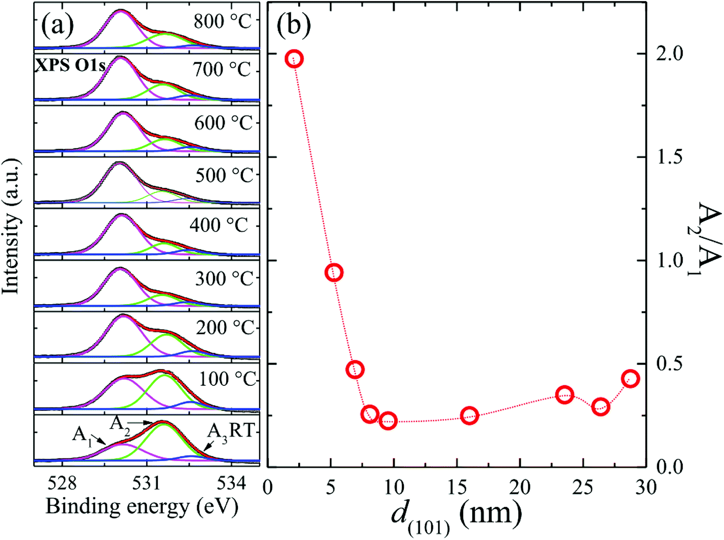
All ZnO films were investigated with XPS to follow the defect evolution caused by annealing. Photoemission signals emerging from the O 1s orbital in ZnO could be attributed to three well-known components, namely, O2− ions in the wurtzite lattice, O2− ions in the oxygen-deficient regions, and surface-chemisorbed O species.35 Spectroscopic deconvolution is exemplified in the inset of Fig. 2(a), indicating area contributions (A1, A2, and A3) corresponding to three components approximately centered at 530.1 eV, 531.6 eV, and 532.7 eV.35 Accordingly, the intensity ratio A2/A1 gives a measure of relative volume of the oxygen-deficient regions and in turn the oxygen vacancy (VO) density in the investigated films. The obtained d(101) dependency of evaluated A2/A1 ratios is shown in Fig. 2(b). It can be seen that the high density of VO in as-deposited films reduced drastically to a low level as the size increased above ∼8 nm (TA = 300 °C). A slight rise in VO density was found for sizes exceeding 16 nm (TA = 500 °C). These findings indicated optimized TA near 400 °C (size ∼ 10 nm), which corresponded to the lowest value of VO density. However, XPS is known as a surface-sensitive method with detection depth limited to about ∼10 nm from the surface. Bulk defects in large grains may become inaccessible when the grain size exceeds the detection depth limit of XPS. Therefore, it can be concluded that the drastic reduction in VO density due to annealing at low TA up to 300 °C (8 nm) mainly occurred in the near-surface region, while most of the as-deposited defects in the core region remained deeply trapped in the bulk. Furthermore, retrogressive increase in A2/A1 determined by XPS with increasing TA from 500 °C to 600 °C revealed an increase in VO density in the near-surface region of relatively large grains, which was accompanied with the recovery of bulk defects, as indicated by a linear increase in EPC strength.32 Our overall results were consistent with those of a report based on PL investigations: annealing nanometer-sized ZnO leads to a reduction in the density of bulk traps while simultaneously creating high density of green-emitting defects in the near-surface region.36 This conclusion corresponded to the poor crystal quality of films annealed from RT to 300 °C and was consistent with XRD, Raman, and PL results, which will be discussed further in the text.
 |
| | Fig. 2 (a) Illustrating spectroscopic deconvolution of three components contained in photoemission signals emerging from the O 1s orbital in ZnO/ALO films (bottom to top: RT to 800 °C); (b) evaluated A2/A1 ratios (oxygen vacancy (VO) density) revealed by XPS with average grain size d(101). | |
3.2. Photoluminescence and emission of confined excitons
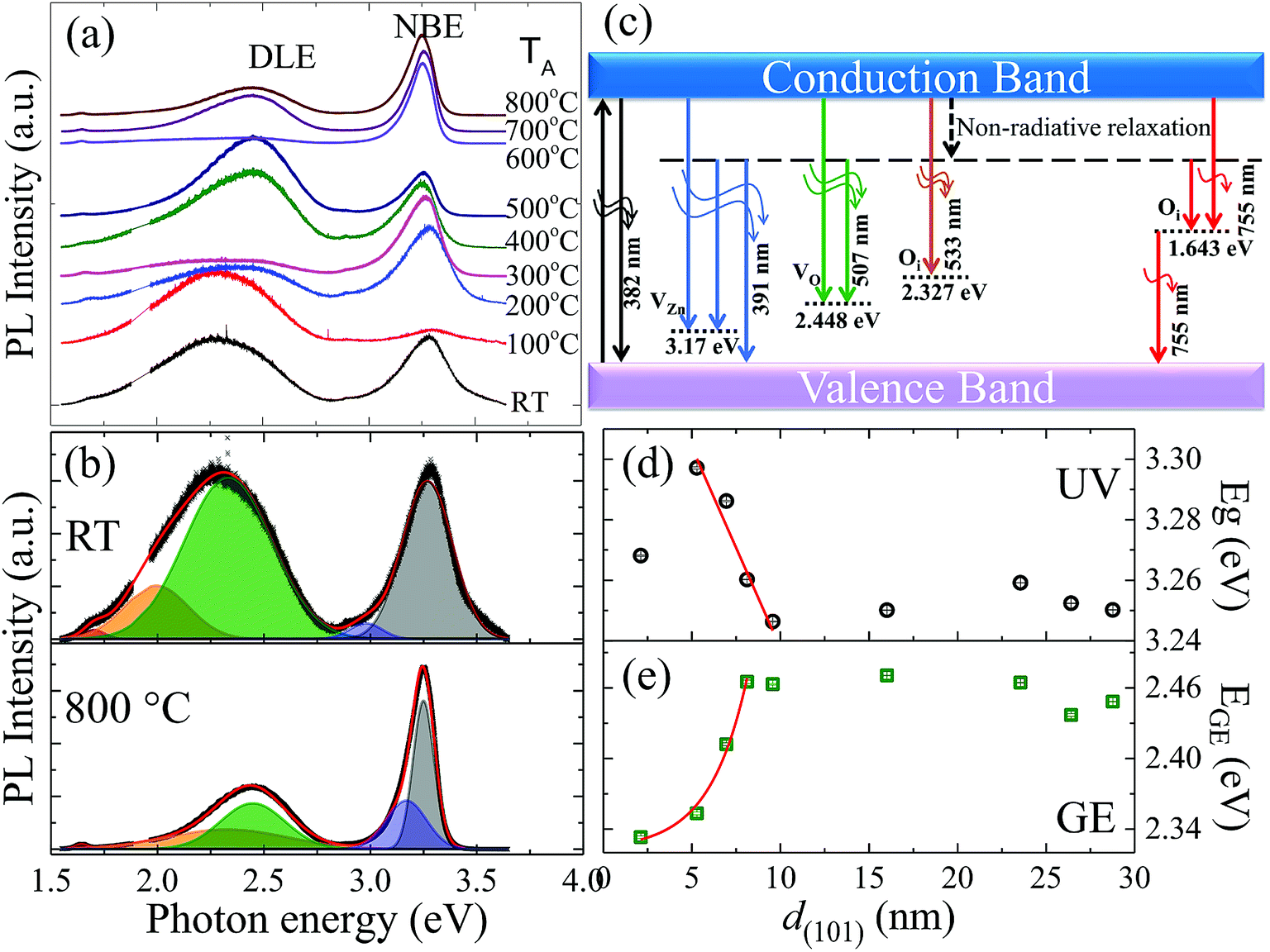
Room-temperature PL spectra of ZnO films, shown in Fig. 3(a) for dependence of TA from RT to 800 °C (bottom to top), were characterized by two main emissions: one in the ultra-violet (UV) region around ∼390 nm (3.2 eV) and the other in the visible region, i.e., ∼520 nm (2.4 eV). The UV emission originated from exciton recombination corresponding to the NBE transition in ZnO, while DLE in the visible region was observed due to recombination of photo-generated holes with gap states associated with various structural defects such as VO, zinc vacancies (VZn) and interstitial defects.29 The NBE intensity exhibited overall decay with decreasing grain radius due to the nonradiative exciton recombination via surface defect states, which was superimposed with a local maximum from 300 °C (8 nm) and 600 °C (26 nm) for the films, the details of which will be discussed further in the text. Fig. 3(b) shows the deconvoluted PL spectra of films annealed at RT and 800 °C using the Voigt distribution function represented by fitted solid lines in the upper and lower panels, respectively. The fitted parameters obtained from various films are summarized in the ESI in Table S2.† Deconvolution of the PL spectra indicated the distinct presence of five individual components, as represented by different shaded colours in Fig. 3(b). Depending on the emission energy from the sample obtained by annealing at 800 °C, the five components were categorized as UV spectrum 3.25 eV (382 nm, grey colour); UV-violet 3.17 eV (391 nm, blue colour); green emission 2.448 eV (507 nm, green colour); orange emission 2.327 (533 nm, orange colour); and red emission 1.643 eV (755 nm, red colour). A schematic plot of various PL emission components originating due to electronic transitions between different defect levels and the band edges of ZnO is given in Fig. 3(c). The UV emission band was associated with the excitonic recombination of electrons in the conduction band (CB) and holes in the valence band (VB), leading to NBE transition. The UV-violet luminescence at 3.17 eV was attributed to VZn and the intense green emission (GE) at 2.448 eV was ascribed to VO. The orange and red luminescences at 2.327 eV and 1.643 eV were related to the possible transitions of trapped electrons at interstitial oxygen sites (Oi) from or to CB and VB.37
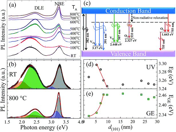 |
| | Fig. 3 (a) Room-temperature PL spectra of ZnO films in dependence of TA from RT to 800 °C (top to bottom). (b) Deconvoluted PL spectra of RT and 800 °C films using the Voigt distribution function represented by fitted solid lines in the upper and lower panels, respectively. (c) A schematic plot of various PL emission components originating due to electronic transitions between different defect levels and the band edge of ZnO films. Grain size d(101) dependency of fitted values of (d) Eg and (e) EGE, where solid lines represent theoretical curves determined using linear and exponential functions given in the main text. | |
NBE of bulk ZnO at RT has been known to be dominated by phonon replicas of free exciton transition with a maximum at the first LO phonon line,38 which can be estimated to be located near 3.24 eV taking into account the well-known bandgap (Eg = 3.37 eV), LO phonon energy (70 meV), and exciton binding energy (60 meV). Compared with the results for the bulk counterpart, our observations of systematic redshifts in Eg from ∼3.30 eV to 3.25 eV with increasing grain size up to ∼10 nm (Fig. 3(d)) can be attributed to quantum confinement effects in nanostructural ZnO.11–14,17–21 Furthermore, defect-state-related broadband DLE has been studied extensively without consensus on its origin.2 The best known GE of photon energy around 2.1–2.5 eV has been attributed to point defects with all types of native defects proposed as candidates.39–41 Annealing hydrothermally grown single crystals at 500–1050 °C in air or in pure oxygen was reported to result in a blueshift of DLE from the as-grown Li-band peaking at 2.17 eV to the VZn-related band at 2.35 eV.39 Another recent study showed that green luminescence in hydrothermally grown single crystals of ZnO has multiple origins, consisting of a band at 2.3 eV due to recombination of electrons from CB with VZn acceptors coupled with hydrogen and a band at 2.47 eV related to VO.40 The authors concluded that annealing in Zn vapor removed VZn and introduced VO, leading to the disappearance of the luminescence band at 2.3 eV and the appearance of GE at a higher energy of 2.47 eV. Our observations were consistent with the investigations on ZnO single crystals;39,40 the DLE maximum (EGE), as shown in Fig. 3(e), exhibits blueshifts from 2.33 eV to the bulk-like value of 2.46 eV with increasing grain size up to ∼10 nm. The size dependency of Eg and EGE up to ∼10 nm can be described very well using a linear function Eg = 3.37(2) − 0.013(3)d(101) and an exponential function EGE = 2.32(1) + 0.003![[thin space (1/6-em)]](https://www.rsc.org/images/entities/char_2009.gif) exp(d(101)/2.1(6)), as represented by solid lines in Fig. 3(d) and (e), respectively. We note that the quantum-effect critical size of dc ∼ 10 nm above which Eg and EGE become size-independent is corroborated by previous Raman scattering analysis showing weakened EPC for small-sized ZnO with d < dc, which has been proposed to result from reduced Fröhlich interactions due to the low polar nature of the spatially confined system.32
exp(d(101)/2.1(6)), as represented by solid lines in Fig. 3(d) and (e), respectively. We note that the quantum-effect critical size of dc ∼ 10 nm above which Eg and EGE become size-independent is corroborated by previous Raman scattering analysis showing weakened EPC for small-sized ZnO with d < dc, which has been proposed to result from reduced Fröhlich interactions due to the low polar nature of the spatially confined system.32
The bulk- or single-crystal-like features of NBE and DLE discussed above are thought to reflect the high purity and high quality of our vapour-phase-deposited and annealed films in contrast to those of the samples prepared using solution-based procedures. Furthermore, mechanisms of GE from ZnO powders have been intensively studied.42,43 Foreman et al. proposed that excitation of GE occurs via formation of localized excitons bound to near-surface defect states,42 whereas Kodama et al. proposed that GE excitation in highly defective and tail-state-rich ZnO is dominated by thermally activated trapping/de-trapping processes associated with optically excited sub-bandgap states.43 It should be noted that significant size-dependent intensity variations of GE-like DLE (2.45 eV) in ZnO nanosheets have been found to correlate with that of exciton emissions, whereas the DLE intensity at 2.05 eV exhibits slight size dependence.44 In our case, tail states are not observed and the PL spectra in Fig. 3 exhibit bulk-like characteristics, as discussed. Thus, from the above-mentioned observations, we conclude that the DLE observed in this study can be identified with defect-induced GE discussed in the literature.
To further deepen the understanding of the luminescent nature of ZnO, the size-dependence of the emission intensities was investigated. Recent research has been focused on quantitatively verifiable models based on reasonable mechanisms and dynamics of the excitonic relaxation processes. The total relaxation rate of excitons is dominated by nonradiative surface and/or interface states in grain boundaries of ZnO microcrystals.27 Taking into account the geometrical factor of size-dependent surface-to-volume ratio, the time-integrated intensity of exciton emission from ZnO grains with an average radius R varying from 20 nm to 1.25 μm was found to reasonably follow the relation27
| | |
I = ηkr(kr + R−1α)−1,
| (1) |
where
kr is the radiative relaxation rate of excitons, and
η and
α are experimentally determined parameters. The solid line in
Fig. 4 represents a best fit to
eqn (1) for NBE intensity (relative ratio) with
kr = 1/455 (10
12 Hz),
α = 1.12 (10
12 Å Hz), and
η = 3.2(5). The significant deviation of the fitted curve from the experimental data in
Fig. 4 shows a failure in extrapolating the validity of
eqn (1) for smaller-sized ZnO investigated in this study. This clearly indicated that the
R−1 rule, which characterizes the bulk-like emission intensity assuming a size-independent relaxation rate
kr, breaks down for ZnO crystals with a radius below a critical size
dc ≈ 2
Rc, as discussed in
Fig. 3(d) and (e). The quantum nature of confined excitons below
dc could significantly modify
kr and lead to peculiar size dependence, overwhelming the
R−1 geometrical factor in the NBE intensity.
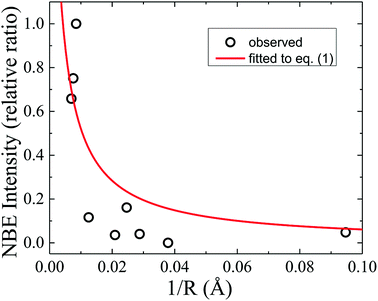 |
| | Fig. 4 NBE intensity (relative ratio) in dependence of the reciprocal average grain radius (1/R), where the solid line represents a theoretical fit using eqn (1). | |
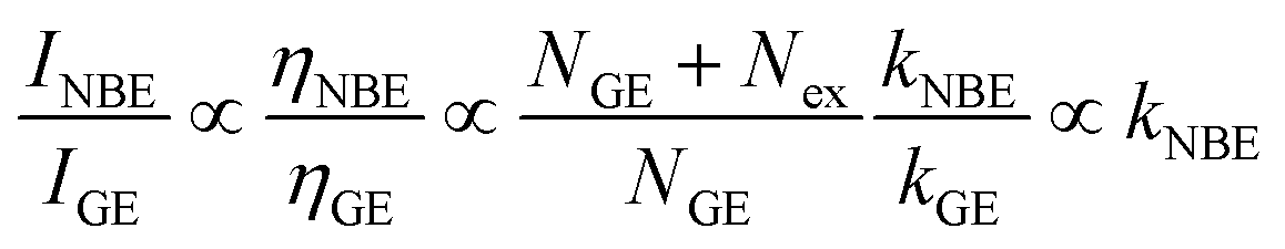
The existence of a direct connection between GE and exciton relaxation processes similar to that proposed by Foreman et al.42 is supported by the fact that GE exhibited similar trends in an overall intensity decay with decreasing R to the exciton-recombination-related NBE intensity, shown with normalization in Fig. 5(a) (filled symbol: NBE; open symbol: GE; dashed and continuous lines are guide for the eye). Assuming that there exists a mechanistic correlation between exciton population and GE efficiency,42 the quantum efficiencies of NBE and GE from ZnO powders are given as26
| |
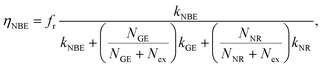 | (2) |
| |
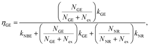 | (3) |
where
Nex,
NNR, and
NGE are densities of photoexcited excitons, non-radiative defects, and GE-active defects, respectively;
kNBE,
kGE, and
kNR represent the rate constants associated with the processes of radiative NBE recombination of excitons, energy transfer from excitons to GE-active defects, and non-radiative recombination, respectively. The factor
fr accounts for the fact that a large fraction of the NBE photons is reabsorbed, whereas the GE photons experience no such parasitic reabsorption. For identical optical transmissions used in all our PL observations, the relative intensities of NBE and GE can be evaluated using
eqn (2) and
(3) as follows:
31| |
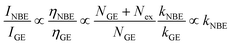 | (4) |
Here,
Nex is considered to be constant under identical excitation conditions and
kGE is presumably independent of crystal size. It was assumed that variations in
NGE due to annealing were weak and negligible. Using the PL results in
Fig. 3(a), the experimentally evaluated
INBE/
IGE is displayed in
Fig. 5(b) for dependence of
R. Both maxima in the original size-dependent NBE intensity in
Fig. 5(a) become more prominent in
Fig. 5(b). This is understood by considering that the effects of the size-correlated density of uniformly distributed
NNR in
eqn (2) and
(3) as well as the intensity fluctuations due to excitation and/or inhomogeneity are suppressed by considering relative intensities. According to
eqn (4), the maxima in
INBE/
IGE observed in
Fig. 5(b) are thought to be dominated by size-dependent exciton decay rates, which are controlled by the intrinsic exciton stability and nonradiative recombination
via surface defect states. Using a one-band electron-three-band hole envelope function model for solving the six-dimensional two-particle problem, Fonoberov
et. al. evaluated the size dependence of exciton radiative lifetime for ZnO QDs having
R = 1 to 3 nm and proposed an analytical approximation for the evaluated exciton radiative lifetime:
τ =
τ0/[1 + (
R/
R0)
3] with
τ0 = 73.4 ps and
R0 = 2.55 nm.
25 The corresponding size-dependence of exciton radiative recombination rate is represented in
Fig. 5(b) (solid line) in the smallest-size region according to
| | |
INBE/IGE ∝ kNBE = C/τ0[1 + (R/R0)3]
| (5) |
where
C = 5 ps,
τ0 = 29.4 ps and
R0 = 2.11 nm represent the experimental constant and fitting parameters. For the intermediate-size region, the size-dependent NBE relaxation rate has been experimentally determined for ZnO grains with an average radius (
R) from 20 nm to 1.25 μm, giving the total rate as follows:
27
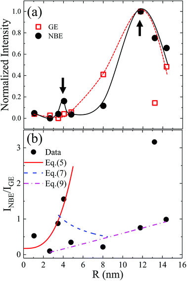 |
| | Fig. 5 (a) Normalized GE and NBE intensities (lines provide a guide to the eye) and (b) relative intensities of NBE and GE in dependence of R. Parameters for fitting the theoretical curves determined using eqn (5), (7), and (9) are given in main text. | |
By extrapolation of eqn (6), the size-dependence of the exciton radiative rate constant for the intermediate confinement region with R varying from 3.5 to 8 nm is represented in Fig. 5(b) (dashed line) according to
| | |
INBE/IGE ∝ kNBE = C(kr + R−1α)
| (7) |
by considering the fitted parameters
kr = 1/455 (10
12 Hz) and
α = 1.12 (10
12 Å Hz) obtained from
eqn (1) and
C = 32.54 ps.
Combining theoretical25 and experimental27 conclusions of exciton lifetime in ZnO QDs, a local minimum in the size-dependent exciton radiative lifetime has been predicted to emerge when R ≈ 5 nm (at 18 K), which is expected to shift to larger dot sizes with increasing temperature.45 However, in this case, even at room temperature, the corresponding maximum of INBE/IGE is found at R ≈ 4 nm, as shown in Fig. 5, which is attributed to the quantum-confinement-induced local minimum in the size-dependent exciton radiative lifetime. The observed second local maximum in the large-sized region can be explained by considering resonant exciton-light coupling. The size dependence of the coupling strength of exciton electronic states with electromagnetic fields in ZnO nanospheres has been studied taking into account the retardation effect or the formation of exciton-polaritons.46 Approximating the exciton wave function with Gaussian form, in the evaluated exciton radiative rate, the authors found a non-monotonous dependence of a nanosphere's radius (r) given as
| |
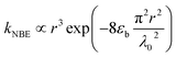 | (8) |
with a resonance maximum expected at
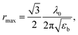
where
εb and
λ0 are the bulk dielectric constant and the light wavelength at an exciton resonance frequency, respectively.
46 Considering
εb = 3.7 and
λ0 ≈ 380 nm, as determined in
Fig. 3, the resonance condition can be evaluated as
rmax = 27 nm, which is around ∼2 times greater than the grain radius (
R′ = 13 nm) at which the second maximum in
INBE/
IGE is observed. Therefore, the correlated onset of structural reconstruction of ZnO crystallites and defect redistribution thermally activated above 600 °C is considered more likely to be the responsible impact;
32 this results in a local minimum in the surface defect density revealed by XPS, as shown in
Fig. 2, in correlation with the second maximum in
INBE/
IGE emerging at
R′. After observing in ZnO nanowires the almost linearly decreasing relative intensity of NBE and GE with decreasing wire radius, Shalish
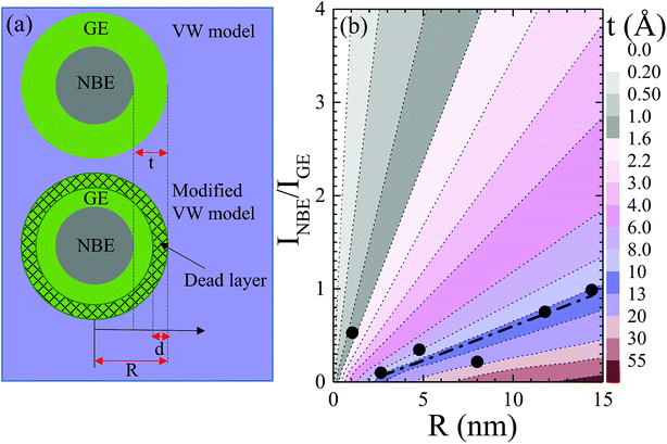
et al. proposed a VW model assuming that a surface layer is responsible for GE, whereas NBE exclusively originates from an interior bulk region.
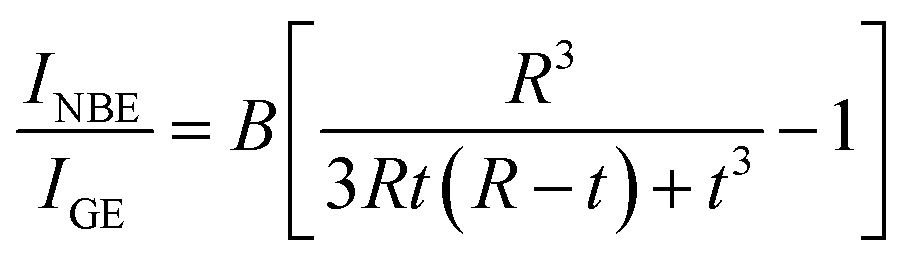
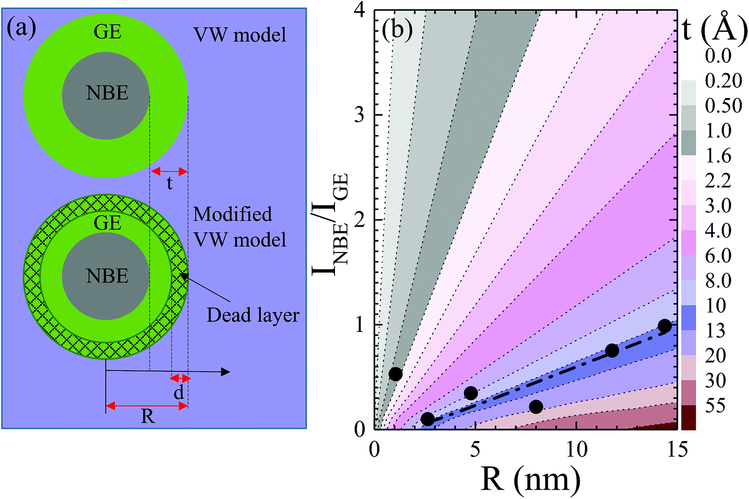
30 A schematic of the layered structure is depicted in the upper panel of
Fig. 6(a) for a cylindrical wire (in cross section) or a spherical nanocrystal having radius
R and a GE-active layer of thickness
t. From the value of
t ≈ 30 nm obtained for nanowires with
R from 50 to 270 nm, it has been suggested that in quantum-sized nanocrystals, GE-related surface recombination may entirely quench band-to-band recombination.
30 In fact, using the VW model, Chaudhuri
et al.47 reported surface layers of
t = 3.6 and 1.5 nm for ZnO rods and platelets (
R = 11.5 to 50 nm) and spherical nanocrystals (
R = 2.5 to 7.5 nm). Ignoring the data points of drastically enhanced
INBE/
IGE near
R = 4 and 13 nm in
Fig. 5(b),
INBE/
IGE observed for a grain radius from 2.5 to 14.5 nm exhibited a nearly linear size dependence. A dash-dot line in
Fig. 5(b) and
6(b) represents a fit by assuming the validity of the VW model
47| |
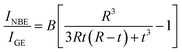 | (9) |
with
t = 1.05 nm and
B = 0.24. The obtained nearly linear size dependence of
INBE/
IGE in the present study and that in the literature
30,47 corroborated the near-surface origin and exciton-related nature of GE in ZnO, disregarding the investigated nanostructure forms. The different colors used in
Fig. 6(b) correspond to the GE-active layer thickness
t, which increases with the increase in
R for a given value of
INBE/
IGE. The observed simulated results are in good agreement with the experimentally determined values of
t in the present study and those reported in the literature,
30,47 indicating a trend of increasing
t with increasing size. From
Fig. 6(b), it can be noted that the observed value of
INBE/
IGE = 0.53 obtained for ZnO grains having
R = 1 nm, which is located in the gray-coloured region with
t ≤ 1.6 nm, deviates significantly from linearity. The observed value of
t obtained for ZnO grains having
R = 1 nm is very close to the theoretically predicted thickness of a surface exciton dead layer,
d ≈ 1.6 nm,
25 with
c-axis excitons squeezed to the nanosphere center.
25 Taking into account that GE originates from exciton relaxation processes
via near-surface defect states,
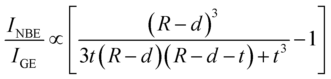
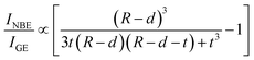
42 GE can be deactivated in a confinement-induced surface exciton dead layer, within which the exciton probability is zero. Accordingly, a modified VW model can predict size dependence in
INBE/
IGE as taking into account a layer structure for a spherical nanocrystal with a size in the intermediate confinement regime, as depicted in the lower panel of
Fig. 6(a). Contrary to the proposed model,
47 our finding of the non-monotonous size dependence of
INBE/
IGE in an intermediate confinement regime (
Fig. 5) cannot be described either by
eqn (9) or
(10) even after considering a nearly linear increasing
d with increasing radius according to theoretical calculations.
25 Jacobsson
et al.11 investigated wet-chemically prepared ZnO QDs with sizes from 3.7 nm to 6.2 nm, realizing measurements of exciton decay rates with higher sampling frequency in dot sizes. They found drastic increase in exciton lifetime from ∼10 ps to ∼30 ps as the dot radius decreased from 2.8 nm to 2.6 nm, which was attributed to quantum-confinement-induced enhancement of exciton stability. Our results are thought to be consistent with the findings reported by Jacobsson
et al.,
11 indicating that the possible effects of defects and impurities due to solution-based preparation can play a role in understanding the discontinuous size dependence in exciton lifetime observed by the authors.
| |
 | (10) |
 |
| | Fig. 6 (a) Layer structure assumed in VW and modified VW model in upper and lower panels, where t, d, and R denote the thickness of the GE-active layer, dead layer of confined excitons and radius of the nanostructure. (b) Simulated plot of relative intensity of NBE and GE in dependence of R using eqn (9), where different colors represent the thickness t of the GE-active layer. The dash-dot line represents a theoretical fit using eqn (9) and corresponding fitting parameters are given in the main text. | |
4. Conclusion
In conclusion, we have investigated the size-dependence of room-temperature PL of high-quality crystalline nanostructured ZnO films with grain sizes varying from 2 to 29 nm fabricated using vapor-phase deposition and post-annealing at different temperatures. The spectral shift and luminescence intensity of NBE and DLE were studied in correlation with structural and defect evolution revealed by XPS and previous studies of XRD and Raman scattering.32 Identifying effects due to annealing-induced redistribution and changes in defect densities, peculiar variations in the size dependence of NBE and DLE were attributed to quantum confinement effects below a critical size, dc ∼ 10 nm. This region is consistent with that where the weakening of EPC has been revealed and proposed to result from reduced Fröhlich interactions due to the low polar nature of the spatially confined system. Moreover, a local maximum in the size-dependent relative intensity of INBE/IGE found at a grain radius R ≈ 4 nm could be related with a theoretically predicted local minimum in the size-dependent exciton radiative lifetime, indicating enhanced emission efficiency due to intrinsic quantum effects of confined excitons. Disregarding the local maxima due to confinement and reconstruction, the nearly linear size dependence of INBE/IGE from 5 to 29 nm suggested an extension of the validity range of the VW model taking into account a 1.05 nm-thick GE-active surface layer. The effects of a theoretically proposed exciton dead layer were discussed in contrast to those of the VW model for the intermediate confinement regime, where the formation of a surface dead layer surrounding confined excitons was corroborated by our size-dependent PL observations. Our results have improved the understanding of photoluminescence properties of ZnO of size down to the confinement regime, where the quantum effects of excitons confined in small crystal dimensions and influences from surface defects cannot be ignored. This new insight in size effects can benefit future photoelectronic device design by taking advantage of the size-controlled stability of confined excitons in nanostructured thin films and luminescent QDs.
Conflicts of interest
There are no conflicts to declare.
Acknowledgements
The authors are grateful to Prof. Sheng Yun Wu of National Dong Hwa University for valuable discussion and help with revising the manuscript. This research was funded by the National Science Council of Taiwan, Republic of China, under grant numbers NSC 99-2112-M-259-007-MY3 and NSC 102-2112-M-259-004.
References
- A. Janotti and C. G. Van de Walle, Rep. Prog. Phys., 2009, 72, 126501–126529 CrossRef.
- U. Ozgur, Y. I. Alivov, C. Liu, A. Teke, M. A. Reshchikov, S. Dogan, V. Avrutin, S. J. Cho and H. Morkoc, J. Appl. Phys., 2005, 98, 041301 CrossRef.
- S. Singh, P. Thiyagarajan, K. M. Kant, D. Anita, S. Thirupathiah, N. Rama, B. Tiwari, M. Kottaisamy and M. S. R. Rao, J. Phys. D: Appl. Phys., 2007, 40, 6312–6327 CrossRef CAS.
- M. Y. Sun, Z. L. Hou, T. Zhang, Z. Wang, W. Shi, R. Lortz and S. Ping, New J. Phys., 2012, 14, 103018 CrossRef.
- X. W. Fu, C. Su, Q. Fu, X. L. Zhu, R. Zhu, C. P. Liu, Z. M. Liao, J. Xu, W. L. Guo, J. Feng, J. Li and D. P. Yu, Adv. Mater., 2014, 26, 2572–2579 CrossRef CAS PubMed.
- M. F. Crommie, C. P. Lutz and D. M. Eigler, Science, 1993, 262, 218–220 CrossRef CAS PubMed.
- Y. Pennec, W. Auwarter, A. Schiffrin, A. Weber-Bargioni, A. Riemann and J. V. Barth, Nat. Nanotechnol., 2007, 2, 99–103 CrossRef CAS PubMed.
- Y. Kayanuma, Phys. Rev. B, 1988, 38, 9797–9805 CrossRef.
- A. van Dijken, J. Makkinje and A. Meijerink, J. Lumin., 2001, 92, 323–328 CrossRef CAS.
- T. J. Jacobsson and T. Edvinsson, J. Phys. Chem. C, 2014, 118, 12061–12072 CrossRef CAS.
- T. J. Jacobsson, S. Viarbitskaya, E. Mukhtar and T. Edvinsson, Phys. Chem. Chem. Phys., 2014, 16, 13849–13857 RSC.
- H. C. Hsu, H. Y. Huang, M. O. Eriksson, T. F. Dai and P. O. Holtz, Appl. Phys. Lett., 2013, 102, 4 Search PubMed.
- K. Suzuki, H. Kondo, M. Inoguchi, N. Tanaka, K. Kageyama and H. Takagi, Appl. Phys. Lett., 2009, 94, 3 Search PubMed.
- G. Pozina, L. L. Yang, Q. X. Zhao, L. Hultman and P. G. Lagoudakis, Appl. Phys. Lett., 2010, 97, 3 CrossRef.
- X. D. Li, T. P. Chen, P. Liu, Y. Liu and K. C. Leong, Opt. Express, 2013, 21, 14131–14138 CrossRef CAS PubMed.
- L. Guo, S. H. Yang, C. L. Yang, P. Yu, J. N. Wang, W. K. Ge and G. K. L. Wong, Appl. Phys. Lett., 2000, 76, 2901–2903 CrossRef CAS.
- W. I. Park, G. C. Yi, M. Kim and S. J. Pennycook, Adv. Mater., 2003, 15, 526–529 CrossRef CAS.
- Y. M. Chang, J. Shieh, P. Y. Chu, H. Y. Lee, C. M. Lin and J. Y. Juang, ACS Appl. Mater. Interfaces, 2011, 3, 4415–4419 CrossRef CAS PubMed.
- H. M. Cheng, K. F. Lin, H. C. Hsu and W. F. Hsieh, Appl. Phys. Lett., 2006, 88, 3 Search PubMed.
- A. Abou Chaaya, R. Viter, I. Baleviciute, M. Bechelany, A. Ramanavicius, Z. Gertnere, D. Erts, V. Smyntyna and P. Miele, J. Phys. Chem. C, 2014, 118, 3811–3819 CrossRef.
- Z. D. Fu, Y. S. Cui, S. Y. Zhang, J. Chen, D. P. Yu, S. L. Zhang, L. Niu and J. Z. Jiang, Appl. Phys. Lett., 2007, 90, 3 Search PubMed.
- V. A. Fonoberov and A. A. Balandin, Appl. Phys. Lett., 2004, 85, 5971–5973 CrossRef CAS.
- S. Yamamoto and T. Mishina, Phys. Rev. B, 2011, 83, 7 Search PubMed.
- S. Baskoutas and G. Bester, J. Phys. Chem. C, 2010, 114, 9301–9307 CrossRef CAS.
- V. A. Fonoberov and A. A. Balandin, Phys. Rev. B, 2004, 70, 5 Search PubMed.
- J. G. Simmons, J. V. Foreman, J. Liu and H. O. Everitt, Appl. Phys. Lett., 2013, 103, 4 CrossRef.
- T. Matsumoto, H. Kato, K. Miyamoto, M. Sano, E. A. Zhukov and T. Yao, Appl. Phys. Lett., 2002, 81, 1231–1233 CrossRef CAS.
- A. W. Cohn, A. M. Schimpf, C. E. Gunthardt and D. R. Gamelin, Nano Lett., 2013, 13, 1810–1815 CrossRef CAS PubMed.
- M. J. Li, G. C. Xing, G. Z. Xing, B. Wu, T. Wu, X. H. Zhang and T. C. Sum, Phys. Rev. B, 2013, 87, 8 Search PubMed.
- I. Shalish, H. Temkin and V. Narayanamurti, Phys. Rev. B, 2004, 69, 4 CrossRef.
- M. Villafuerte, J. M. Ferreyra, C. Zapata, J. Barzola-Quiquia, F. Iikawa, P. Esquinazi, S. P. Heluani, M. M. de Lima and A. Cantarero, J. Appl. Phys., 2014, 115, 5 CrossRef.
- A. Gandhi, W.-S. Yeoh, M.-A. Wu, C.-H. Liao, D.-Y. Chiu, W.-L. Yeh and Y.-L. Huang, Nanomaterials, 2018, 8, 632 CrossRef PubMed.
- I. Shalish, H. Temkin and V. Narayanamurti, Phys. Rev. B, 2004, 69, 245401 CrossRef.
- M. Wojdyr, J. Appl. Crystallogr., 2010, 43, 1126–1128 CrossRef CAS.
- M. Chen, X. Wang, Y. H. Yu, Z. L. Pei, X. D. Bai, C. Sun, R. F. Huang and L. S. Wen, Appl. Surf. Sci., 2000, 158, 134–140 CrossRef CAS.
- J. V. Foreman, H. O. Everitt, J. Yang, T. McNicholas and J. Liu, Phys. Rev. B, 2010, 81, 10 CrossRef.
- V. Kumar, O. M. Ntwaeaborwa, T. Soga, V. Dutta and H. C. Swart, ACS Photonics, 2017, 4, 2613–2637 CrossRef CAS.
- W. Shan, W. Walukiewicz, J. W. Ager, K. M. Yu, H. B. Yuan, H. P. Xin, G. Cantwell and J. J. Song, Appl. Phys. Lett., 2005, 86, 3 Search PubMed.
- T. M. Borseth, B. G. Svensson, A. Y. Kuznetsov, P. Klason, Q. X. Zhao and M. Willander, Appl. Phys. Lett., 2006, 89, 262112 CrossRef.
- J. Cizek, J. Valenta, P. Hruska, O. Melikhova, I. Prochazka, M. Novotny and J. Bulir, Appl. Phys. Lett., 2015, 106, 4 CrossRef.
- C. Ton-That, L. Weston and M. R. Phillips, Phys. Rev. B, 2012, 86, 5 CrossRef.
- J. V. Foreman, J. G. Simmons, W. E. Baughman, J. Liu and H. O. Everitt, J. Appl. Phys., 2013, 113, 7 CrossRef.
- K. Kodama and T. Uchino, J. Phys. Chem. C, 2014, 118, 23977–23985 CrossRef CAS.
- T. V. Torchynska and B. El Filali, J. Lumin., 2014, 149, 54–60 CrossRef CAS.
- V. A. Fonoberov and A. A. Balandin, Appl. Phys. Lett., 2005, 86, 2 CrossRef.
- B. Gil and A. V. Kavokin, Appl. Phys. Lett., 2002, 81, 748–750 CrossRef CAS.
- S. K. Chaudhuri, M. Ghosh, D. Das and A. K. Raychaudhuri, J. Appl. Phys., 2010, 108, 7 CrossRef.
Footnote |
| † Electronic supplementary information (ESI) available. See DOI: 10.1039/c8ra09370a |
|
| This journal is © The Royal Society of Chemistry 2019 |
Click here to see how this site uses Cookies. View our privacy policy here. 
 Open Access Article
 This Open Access Article is licensed under a Creative Commons Attribution-Non Commercial 3.0 Unported Licence
 ,
Ching-Hao Liao,
Wei-Li Yeh and
Yue-Lin Huang
,
Ching-Hao Liao,
Wei-Li Yeh and
Yue-Lin Huang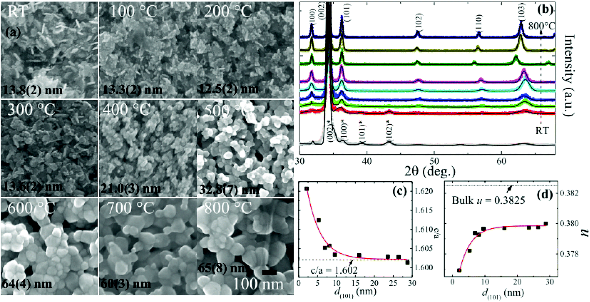


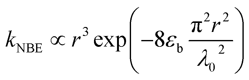
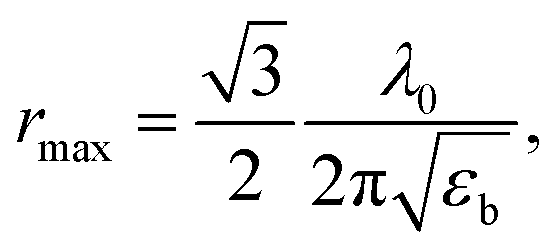 where εb and λ0 are the bulk dielectric constant and the light wavelength at an exciton resonance frequency, respectively.46 Considering εb = 3.7 and λ0 ≈ 380 nm, as determined in Fig. 3, the resonance condition can be evaluated as rmax = 27 nm, which is around ∼2 times greater than the grain radius (R′ = 13 nm) at which the second maximum in INBE/IGE is observed. Therefore, the correlated onset of structural reconstruction of ZnO crystallites and defect redistribution thermally activated above 600 °C is considered more likely to be the responsible impact;32 this results in a local minimum in the surface defect density revealed by XPS, as shown in Fig. 2, in correlation with the second maximum in INBE/IGE emerging at R′. After observing in ZnO nanowires the almost linearly decreasing relative intensity of NBE and GE with decreasing wire radius, Shalish et al. proposed a VW model assuming that a surface layer is responsible for GE, whereas NBE exclusively originates from an interior bulk region.30 A schematic of the layered structure is depicted in the upper panel of Fig. 6(a) for a cylindrical wire (in cross section) or a spherical nanocrystal having radius R and a GE-active layer of thickness t. From the value of t ≈ 30 nm obtained for nanowires with R from 50 to 270 nm, it has been suggested that in quantum-sized nanocrystals, GE-related surface recombination may entirely quench band-to-band recombination.30 In fact, using the VW model, Chaudhuri et al.47 reported surface layers of t = 3.6 and 1.5 nm for ZnO rods and platelets (R = 11.5 to 50 nm) and spherical nanocrystals (R = 2.5 to 7.5 nm). Ignoring the data points of drastically enhanced INBE/IGE near R = 4 and 13 nm in Fig. 5(b), INBE/IGE observed for a grain radius from 2.5 to 14.5 nm exhibited a nearly linear size dependence. A dash-dot line in Fig. 5(b) and 6(b) represents a fit by assuming the validity of the VW model47