
 Open Access Article
 This Open Access Article is licensed under a Creative Commons Attribution-Non Commercial 3.0 Unported Licence
Magneto-EELS of armchair boronitrene nanoribbons
P. T. T.
Le
*ab,
K.
Mirabbaszadeh
 *c and
M.
Yarmohammadi
*c
*c and
M.
Yarmohammadi
*c
aLaboratory of Magnetism and Magnetic Materials, Advanced Institute of Materials Science, Ton Duc Thang University, Ho Chi Minh City, Viet Nam. E-mail: lethithuphuong@tdtu.edu.vn
bFaculty of Applied Sciences, Ton Duc Thang University, Ho Chi Minh City, Viet Nam
cDepartment of Energy Engineering and Physics, Amirkabir University of Technology, Tehran, Iran. E-mail: mirabbas@aut.ac.ir; my69@aut.ac.ir
First published on 21st January 2019
Abstract
The evolution of the electron energy loss spectrum (EELS) of ultranarrow armchair boron nitride nanoribbons (aBNNRs) during low and high photon energy transfers has been studied theoretically when a magnetic field and temperature gradient are applied. In order to achieve this goal, the widely used linear response theory within the Green’s function theory was employed. Here, using the EELS we show that σ ↦ σ* or π ↦ π* and σ ↦ π* or π ↦ σ* excitations corresponding to the intraband and interband transitions, respectively, can be tuned by ribbon width, magnetic field, wave vector transfer, and temperature. A comparison with experimental studies reveals that for realistic ribbon widths, i.e. 10–100 nm, both excitations are weak. However, we observe that only transitions between the same states, i.e. σ ↦ σ* or π ↦ π* can be controlled with a magnetic field due to the localized highest occupied and lowest unoccupied states at low-energy regions and different states are not influenced when the magnetic field is applied. Interestingly, the detailed shape of the magneto-EELS of the 7-aBNNR indicates a direct-to-indirect band gap transition when the wave vector transfer is perpendicular to the 7-aBNNR plane. Finally, we discover that there is an anomalous behavior for the temperature dependence of the magneto-EELS in general. The present work brings forward the understanding of the magneto-EELS of ultranarrow aBNNRs under different environmental conditions for logic applications in nanoplasmonics.
1 Introduction
In the nanoscience and/or nanotechnology communities, tuning the novel properties of low-dimensional materials in a systematically controlled way has been actively researched in recent years. Graphene, a two-dimensional (2D) single atomic layer of graphite had/has been a major breakthrough in nanoelectronics1–5 because of its massless relativistic Dirac fermions with linear dispersion band energy (gapless), which result in high mobility even at T ≃ 300 K. In order for it to be applicable in industry, carving graphene into one-dimensional (1D) nanoribbons was one of the successful ways to tune the electronic properties of graphene.6–16 In addition to graphene, the quasi-1D analogs of other group IV, III–V, and II–VI honeycomb structures are currently the subject of hot research in various fields owing to their intriguing physical properties. By truncating the direction of quasi-1D materials, nanoribbons can mainly be classified into two armchair and zigzag nanoribbons.2D monolayer hexagonal boron nitride (h-BN) as one of the members of the 2D family has attracted much more research attention compared to graphene because graphene is a gapless semimetal, while h-BN is a wide band gap insulator of about 4.5–6 eV (ref. 1, 2 and 17–23) with a superior thermal stability of about 1000 K.24–26 The mismatch between graphene lattices and h-BN lattices is about 2%.27,28 However, tuning the wide band gap of h-BN is/was an interesting research topic. For instance, it has been shown that vacancies in h-BN significantly affect the electronic structure of h-BN.29–34 Additionally, by applying an external electric field, the band gap of h-BN can be controlled.35,36 A protective coating, and transparent and deep ultraviolet emission are the spectacular chemical properties of h-BN.37 These properties have been featured in real applications of h-BN in electro-optical devices.38,39
Nowadays, BN nanoribbons (BNNRs) have been synthesized by unwrapping BN nanotubes into armchair BNNRs (aBNNRs) and zigzag BNNRs (zBNNRs).40,41 The superior thermal stability of about 1000 K of BNNRs also implies that BNNRs are more resistant to oxidation than graphene.19,40 Theoretical studies have reported that aBNNRs (zBNNRs) are semiconductors with a direct (indirect) band gap.35,36 The band gap in aBNNRs oscillates with the ribbon width, whereas it decreases in zBNNRs when the ribbon width is increased. In the past few years, numerous works have been published on the physical properties of BNNRs in the presence of an electric field,35,36 chemical functionalizations,42–44 uniaxial strain,45,46etc. However, to the best of our knowledge, theoretical calculations on the physical properties of BNNRs under a magnetic field under different conditions have not been performed yet.
The fascinating optical properties of low-dimensional nanomaterials (2D or quasi-1D) in the plasmonic community have led to real applications such as nanophotonic devices,47,48 catalysis,49,50 sensing and spectroscopy,51,52 lighting,53,54 and solar energy conversion and storage.55,56 Among the optical properties, reflectivity, refractive index, and absorption spectra can be studied, which are all derived by the dielectric function ε(ω,![[q with combining right harpoon above (vector)]](https://www.rsc.org/images/entities/i_char_0071_20d1.gif) ) (ω and are the frequency and momentum of the light, respectively) of the sample. The electron energy loss spectrum (EELS) in transmission electron microscopy measurements is one of the ideal tools to study electronic excitations in materials.57–61 In addition, EELS tells us how the energy of scattered electrons is changed from perturbations, in which this, in turn, characterizes the inelastic scattering process. As for low-dimensional materials, recently, EELS in graphene, h-BN, transition metal dichalcogenides, and bulk black phosphorus has been studied well.62–67 Theoretically, EELS is the imaginary part of the inverse of the dielectric function L(ω,) = Im[−1/ε(ω,)]. The main aim of the present work is to find out some information about the charge excitations in aBNNRs with the aid of EELS.
) (ω and are the frequency and momentum of the light, respectively) of the sample. The electron energy loss spectrum (EELS) in transmission electron microscopy measurements is one of the ideal tools to study electronic excitations in materials.57–61 In addition, EELS tells us how the energy of scattered electrons is changed from perturbations, in which this, in turn, characterizes the inelastic scattering process. As for low-dimensional materials, recently, EELS in graphene, h-BN, transition metal dichalcogenides, and bulk black phosphorus has been studied well.62–67 Theoretically, EELS is the imaginary part of the inverse of the dielectric function L(ω,) = Im[−1/ε(ω,)]. The main aim of the present work is to find out some information about the charge excitations in aBNNRs with the aid of EELS.
To this end, based on the empirical tight-binding model, we theoretically investigated the effect of a magnetic field on the EELS of n-aBNNRs (n characterizes the ribbon width) that were subjected to light characterized by the energy ℏω and the wave vector . As is known, in EELS experiments, the sample is subjected to an electron beam, not a photon beam, but the model in the present work uses an incident photon beam as a proxy to obtain the EELS response for the host electron–guest light interactions. Further to the ribbon width, temperature and the incident wave vector can be varied to engineer the magneto-EELS in aBNNRs. It should be noted that in our formulation, the magnetic field couples to the electron spin and affects the electronic hopping energy between nearest neighbor atoms B and N. We show the main features of the present paper through the linear response theory and the Green’s function method to address the dielectric response function of the system. Here, it is assumed that the interactions between the atoms B and N and the magnetic field, the light, and the temperature gradient do not change the stability of the system.
This paper is organized as follows: Section 2 presents the tight-binding Hamiltonian model and the Green’s function elements between the different atoms B and N. Then, in Section 3, the dielectric response function is calculated using density–density auto-correlation functions. The numerical results are explained and analyzed in Section 4 when the system is subjected to light, magnetic field, and temperature gradient. Finally, we finish the paper with a summary of the text in Section 5.
2 Empirical tight-binding model and Green’s function theory
In this section we use the same theory applied in our previous work68 to describe the tight-binding Hamiltonian model consisting of the nearest-neighbor hopping terms and the magnetic field term applied to the system perpendicularly for an infinite quasi-1D aBNNR. In our formulation, the periodic conditions are considered along the y direction, while the translational symmetry is along the x direction (see Fig. 1). Thus, the total Hamiltonian is given by
 | (1) |
![[b with combining circumflex]](https://www.rsc.org/images/entities/i_char_0062_0302.gif) is the annihilation (creation) operator for an electron at the i-th site of the lattice. t = 1.95 eV is the hopping integral energy between the nearest neighbor atoms with the on-site energies εB0 = 0 eV and εN0 = −4.57 eV.70 The parameters g, μB, and
is the annihilation (creation) operator for an electron at the i-th site of the lattice. t = 1.95 eV is the hopping integral energy between the nearest neighbor atoms with the on-site energies εB0 = 0 eV and εN0 = −4.57 eV.70 The parameters g, μB, and  are the degeneracy number (the so-called Lande g-factor), the Bohr magneton, and the external magnetic field strength, respectively. It is worth noting that in our calculations, all energy potentials are given in the unit of eV. For this reason, we have no value for the g-factor in the present paper and we set the constants to unity to simplify the simulations, which will be explained later.
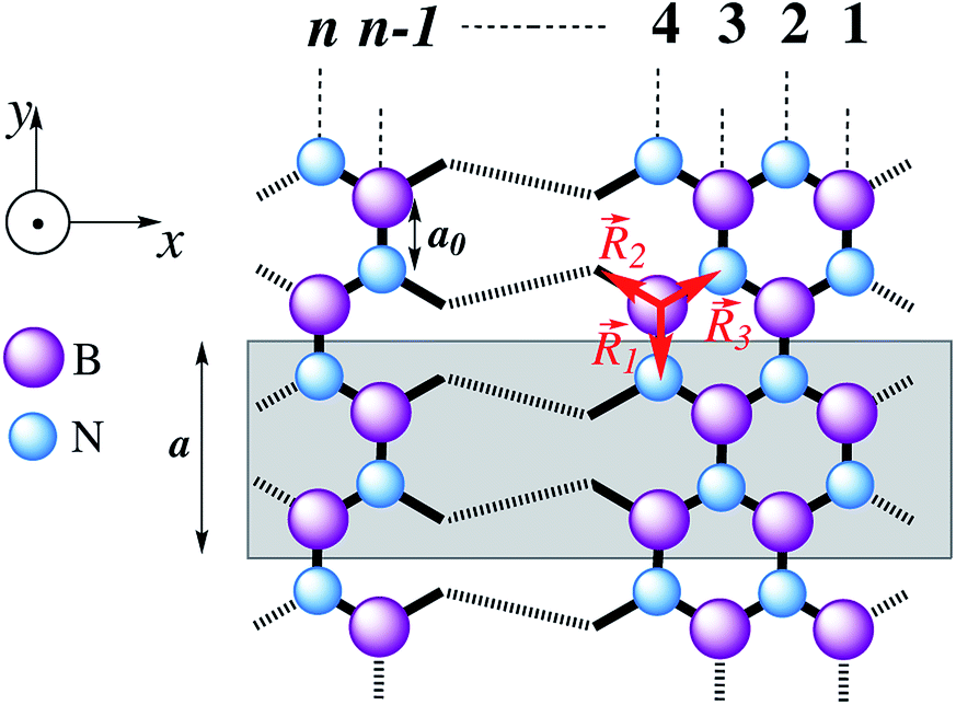 | ||
Fig. 1 Sketch of the top view of the n-aBNNR. The different colors of atom apply to boron (violet) and nitrogen (blue). The bond length a0 in the h-BN is about 1.45 Å.69 The unit cell is shown with a gray box and a = 3a0 is the width of the unit cell, while 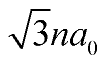 refers to the ribbon width. The vectors refers to the ribbon width. The vectors ![[R with combining right harpoon above (vector)]](https://www.rsc.org/images/entities/i_char_0052_20d1.gif) {1,2,3} connect the nearest neighbors and the symbol ⊙ stands for the applied Zeeman magnetic field direction, i.e. the z direction. {1,2,3} connect the nearest neighbors and the symbol ⊙ stands for the applied Zeeman magnetic field direction, i.e. the z direction. | ||
When the magnetic field is applied the orbital states of the valence band maximum (VBM) and the conduction band minimum (CBM) are influenced, leading to a change in the hopping integral parameter t. This change is given by the Peierls phase factor ΔΦu,m as tu,m = te2πiΔΦu,m. The phase factor appearing in tu,m is calculated by a line integral of the vector potential 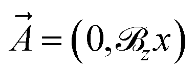 (Landau gauge) via71
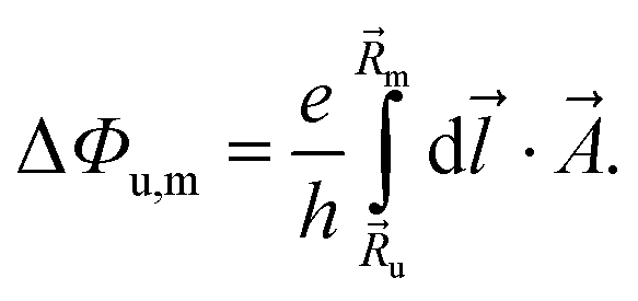 | (2) |
1 = (0,−1)a0,  , and
, and  with a0 = |u,m| = 1.45 Å are the electron charge, the Planck constant, and the vectors corresponding to the nearest neighbor atoms, respectively (see Fig. 1). Although in the numerical calculations, we figured out that the values of tu,m and t are so close to each other, however; we change t ↦ tu,m and deal with tu,m in the Hamiltonian (1) hereafter.
We formulated the tight-binding model in the reciprocal space in order to handle the Hamiltonian more easily. B and N sublattices are called A and B in the following. To this end, we first needed the Fourier transformation of annihilation and creation operators and basis sets |A,kx,ky〉 = ψA(kx,ky) and |B,kx,ky〉 = ψB(kx,ky) for the sublattices A and B, respectively. Each index site i in Fig. 1 can be labelled with two other indices m and sublattices Al and Bl for l ∈ [1,n]. Thus, we used
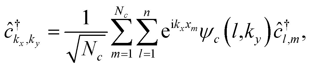 | (3) |
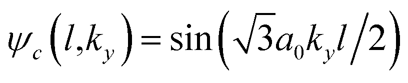 with the discretized vertical wave vector
 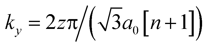 , where z = {1,2,3…n}. From the Hamiltonian in the reciprocal space, we yield the band dispersion energy
 | (4) |
 | (5) |
![[k with combining right harpoon above (vector)]](https://www.rsc.org/images/entities/i_char_006b_20d1.gif) = (kx,ky) belong to the first Brillouin zone (FBZ) of the aBNNR structure.
= (kx,ky) belong to the first Brillouin zone (FBZ) of the aBNNR structure.
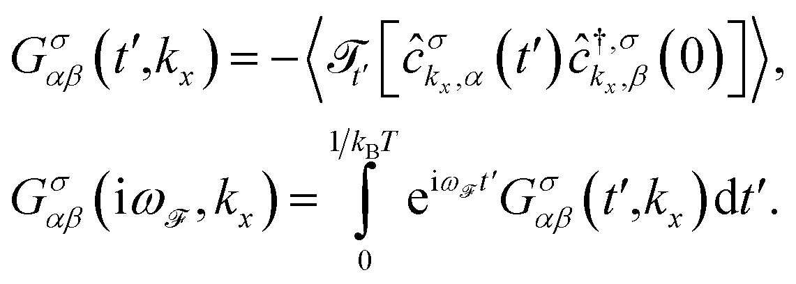
Now we calculate the Green’s function elements using the particle–particle correlation function within the Matsubara formalism73 for {α,β} ∈ {A,B},
 | (6) |
 stands for the time-ordering operator, and
 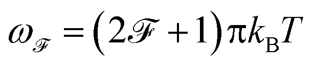 is the fermionic Matsubara frequency (kB is the Boltzman constant and T is the absolute temperature). Finally, by means of tracing over the imaginary part of Green’s function, the electronic density of states (DOS) for
  was calculated by
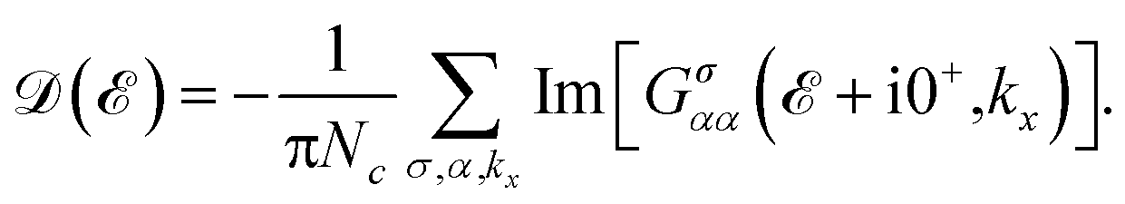 | (7) |
The electronic properties of the 7-aBNNR (arbitrary, only to confirm our formulation) in the absence of the magnetic field are presented in Fig. 2. The left panel refers to the electronic band structure, whereas the right panel shows the electronic DOS. The electron–hole symmetry in the 14-band structure is evident. The macroscopically degenerate states in the valance and conduction bands correspond to the van Hove singularities (peaks) in the electronic DOS. As can be seen, the 7-aBNNR is an insulator system with a band gap of about 4.5 eV for the width corresponding to n = 7, which is in good agreement with ref. 70. In the next section, the dynamical response function of the system is studied using the Green’s functions derived in eqn (6).
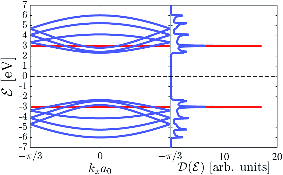 | ||
| Fig. 2 The electronic band structure (left panel) and density of states (right panel) of the 7-aBNNR. The band gap is about 4.5 eV. In the electronic DOS panel, the van Hove singularities corresponding to the flat bands are shown by the red peaks, i.e. the degenerate states. The dashed line is the Fermi level. | ||
3 Dielectric response function
As mentioned, the main features of our study are given by the dielectric response function of the system when subjected to applied light, a temperature gradient, and a magnetic field. To this end, we first calculated the density–density response function within the linear response theory,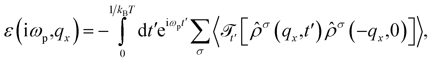 | (8) |
![[small rho, Greek, circumflex]](https://www.rsc.org/images/entities/i_char_e0b7.gif) σ(qx) refers to the charge density operator, defined by
σ(qx) refers to the charge density operator, defined by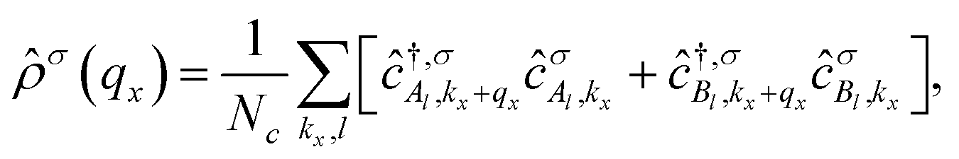 | (9) |
Thus, using Wick’s theorem,73 each element of ε(iωp,qx) is obtained via
 | (10) |
 | (11) |
Finally, the EELS can be calculated easily in terms of both the real and imaginary parts as
 | (12) |
In what follows, we simplified the terms including the fermionic and bosonic Matsubara frequencies using the following approximations of −6 eV ≤ ε ≥ +6 eV and 0 eV ≤ ℏω ≤ 10 eV,
 | (13a) |
 | (13b) |
4 Numerical results and discussion
In this section, we intend to report theoretically the calculated EELS for the n-aBNNRs, which are more or less applicable to other semiconductor aNRs as well. In the present paper we set all physical constants ℏ, kB, g, μB, e, and me to unity for simplicity. For this reason, the quantities here are in their main units, e.g. leads to
  . On the other hand, we are interested in the units of eV for all energy potentials in our simulations. This implies that one can convert the units simply to the main ones. Additionally, it should be pointed out that we studied ultranarrow aBNNRs (1–3 nm), which can only be imagined to be synthesized via bottom-up methods in experiments. We have chosen these ribbon widths because we want to separate the intra- and interband transitions clearly and this needs a wide band gap, which leads to remarkable optical properties.74 For realistic ribbon widths (10–100 nm), the band gap is much less than 1–3 nm in our calculations and transition separation is a little bit complicated. It is necessary to note that the systems under study here are supposed to be optimized before and after applying the magnetic field, the light, and the temperature gradient.
Let us briefly describe the main points appearing in the EELS plots. Obviously, the electronic excitation and transition between the different bands in a system depend strongly on energy (ℏω) and wave vector (qx) transfer. All of the curves are inside the visible region of the electromagnetic spectrum from 0 to 10 eV. In a nutshell, the highest valence bands and the lowest conduction bands are characterized in terms of the σ and π states, the so-called covalent (in-plane) and van der Waals bonding (out-of-plane), respectively. The transition between bands can be classified into three categories: (i) the intraband transitions for very low-energy ℏω with σ ↦ σ* or π ↦ π*, (ii) the interband transitions for the low or intermediate energy region with σ ↦ π* or π ↦ σ*, and (iii) inner-shell ionization for the high energy region with π + σ or π* + σ* excitations. The latter is out of the scope of the present work and needs further study, which most probably will be considered for our future research. The analysis of the results in the following is done using the first two selection rules above, i.e. (i) and (ii).
In what follows, first the EELS of the n-aBNNRs with and without the magnetic field are investigated for different widths in order to see what the ribbon width effect is on the EELS. Afterward, we concentrate on the effect of the magnetic field, the wave vector transfer qx, and the temperature on the frequency transfer-dependent EELS of the 7-aBNNR. It is worth noting that the behavior of the response function originates strongly from the dispersion energy of the aNRs (see eqn (3)). On the other hand, one can see from the band structure shown in Fig. 2 that there is a relationship between the ℏω of the light and the band gap of the system. This means that depending on the value of ℏω, the type of transition is determined. Generally, the lower bound of the interband transitions is exactly the band gap size of the system, which is evident in all figures in the following (ℏω ≃ 4.5 eV).
In Fig. 3, we report the EELS as a function of the energy transfer ℏω for the aBNNRs in three different ribbon widths corresponding to n = 4, 10, and 16 when the magnetic field is absent or present. Definitely, based on other studies such as the work by Galambosi et al.,75 no intraband transition is expected but interestingly, the accuracy of our calculations gives us some important information about the intraband transitions, which is hard to see in experiment. Fig. 3(a) shows the EELS in the absence of the magnetic field. The peaks below ℏω ≃ 4.5 eV are mainly caused by the intraband transitions for the σ ↦ σ* or π ↦ π* states, in which their intensities decrease with an increase in ribbon width. This means that for more realistic ribbon widths, there is no intraband transition in good agreement both theoretically and experimentally with ref. 75 and 76. The next remarkable point shown in Fig. 3(a) refers to the interband transitions for the σ ↦ π* or π ↦ σ* states, in which again the height of the corresponding peaks decreases with n. In both the intra- and interband transitions, the number of peaks increases with n stemming from the ribbon width-dependent dispersion energy of the aNRs (see eqn (3)). On the other hand, the heights of the peaks in the absence of the magnetic field in the low- and intermediate regions are almost the same at certain n values. While it seems that there is no change in the interband transition peak intensity for the σ ↦ π* or π ↦ σ* states when  , interestingly, the peak intensity for the intraband transitions increases as soon as the magnetic field is switched on, as shown in Fig. 3(b). This implies that when the magnetic field is applied, the highest occupied and the lowest empty states in the aBNNRs do not become localized, whereas when an electric field is applied, they become localized, leading to a change in the interband transitions.
 | ||
Fig. 3 EELS of the n-aBNNR as a function of the energy transfer ℏω for different ultranarrow ribbon widths corresponding to n = 4, 10, and 16 in the (a) absence and (b) presence of a magnetic field  . The wave vector transfer and the thermal energy were fixed at |qxa0| = π/6 and kBT = 0.5 eV, respectively. . The wave vector transfer and the thermal energy were fixed at |qxa0| = π/6 and kBT = 0.5 eV, respectively. | ||
To confirm the amazing behavior of the intra- and interband transitions in the presence of the magnetic field, the EELS of the 7-aBNNR under different magnetic field strengths are represented in Fig. 4. From this figure, it is clear that only the low-energy EELS corresponding to the σ ↦ σ* or π ↦ π* excitations of the 7-aBNNR is influenced by the magnetic field and the σ ↦ π* or π ↦ σ* ones are not changed. This result tells the experimentalists that to observe these kinds of excitation in aNRs in the presence of a magnetic field, very low photon energies up to ℏω ≃ 2 eV are required and the excitations are well described in terms of bound electrons in σ or π states. In the next part, we intend to investigate the effect of wave vector transfer qx and temperature on the EELS of the 7-aBNNRs in a constant magnetic field  .
.
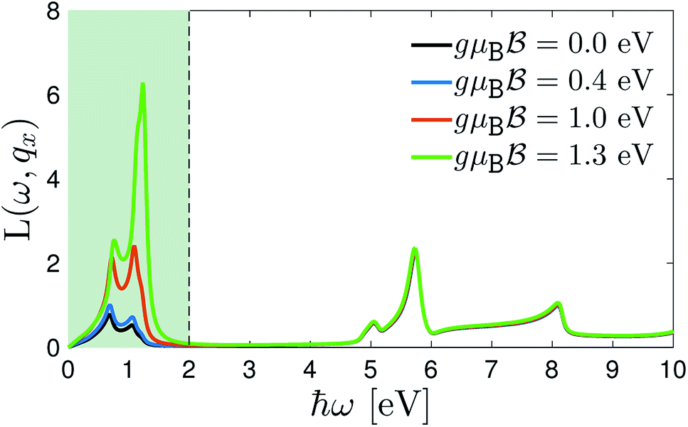 | ||
Fig. 4 Magneto-EELS of the 7-aBNNR at |qxa0| = π/6 and kBT = 0.5 eV when different magnetic field potentials are applied, namely  . The magneto-intraband transitions are evident in the shadowed area. . The magneto-intraband transitions are evident in the shadowed area. | ||
Fig. 5 shows the valence excitation spectra of the 7-aBNNR in the presence of a magnetic field  and a thermal voltage kBT = 0.5 eV when the system is subjected to different directions of light. In short, the qx-dependent EELS affects the transitions significantly. In the studies by Tarrio and Schnatterly76 and also Tosatti and Bassani,77 it has been shown that with in the plane (perpendicular to the plane), only the transitions between the bands of the same (different) states, σ ↦ σ* or π ↦ π* (σ ↦ π* or π ↦ σ*), are allowed. Interestingly, as shown in Fig. 5, our results showcase the same results for the case of the same states at |qxa0| = π/6, whereas this happens at |qxa0| = π/2 for the case of different states, i.e. the black and green curves, respectively. The intraband transitions for |qxa0| = π/6 emerge during lower energy transfers compared to |qxa0| = π/2, while in the case of interband transitions, the wave vector |qxa0| = π/2 is dominant. On the other hand, from the lower bound of the interband transitions, one can conclude that a direct-to-indirect band gap transition occurs when the wave vector transfer is perpendicular to the plane. This can be understood from this fact: assume that
  ,
,  , and kx are the VBM, the CBM, and the wave vector of electrons when the system is not subjected to light (see Fig. 2). When kx ↦ kx ± qx,
  and
and  will appear in different values (see eqn (3)) and this means that the direct band gap at kx is converted to an indirect one due to the kx ↦ kx ± qx, transfer.
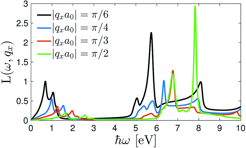 | ||
Fig. 5 Magneto-EELS of the 7-aBNNR when the direction of incident light is changed, namely |qxa0| = π/6, π/4, π/3, and π/2 at a thermal voltage kBT = 0.5 eV and an applied magnetic field  . The direct-to-indirect band gap transition can be viewed by the shift of the zero region of the EELS and the peak intensities. . The direct-to-indirect band gap transition can be viewed by the shift of the zero region of the EELS and the peak intensities. | ||
In a similar fashion, we finish the paper by reporting the temperature effects on the EELS of the 7-aBNNR at |qxa0| = π/6 and  , as shown in Fig. 6. The temperature dependence of the EELS demonstrates an anomalous behavior in two photon energy regions, 1 eV < ℏω < 3 eV and 5 eV < ℏω < 6 eV. At all energies, the EELS increases slightly with temperature but at very low energy regions, the changes are not significant in comparison to the two other regions mentioned above. This, in turn, tells us that the σ ↦ σ* or π ↦ π* excitations are not affected by the temperature gradient, while the other σ ↦ π* or π ↦ σ* excitations at higher energies undergo more alterations when the temperature is increased. It can be seen from Fig. 6 that, while there are weak peaks at low temperatures, in both regions the EELS curves exhibit a clear maximum at kBT = 11.5 eV. To elucidate the origin of these anomalous behaviors, we need a strong experiment to investigate in detail the complexity of the processes. However, we simply report such anomalous behavior originating from the competition between the thermal and quantum effects. In other words, at low photon energy regions, the scattering rate of the host electrons is much less than that at higher regions and temperature affects the kinetic energy of the carriers (and eventually the scattering rate quantity), leading to higher intensities of the EELS.
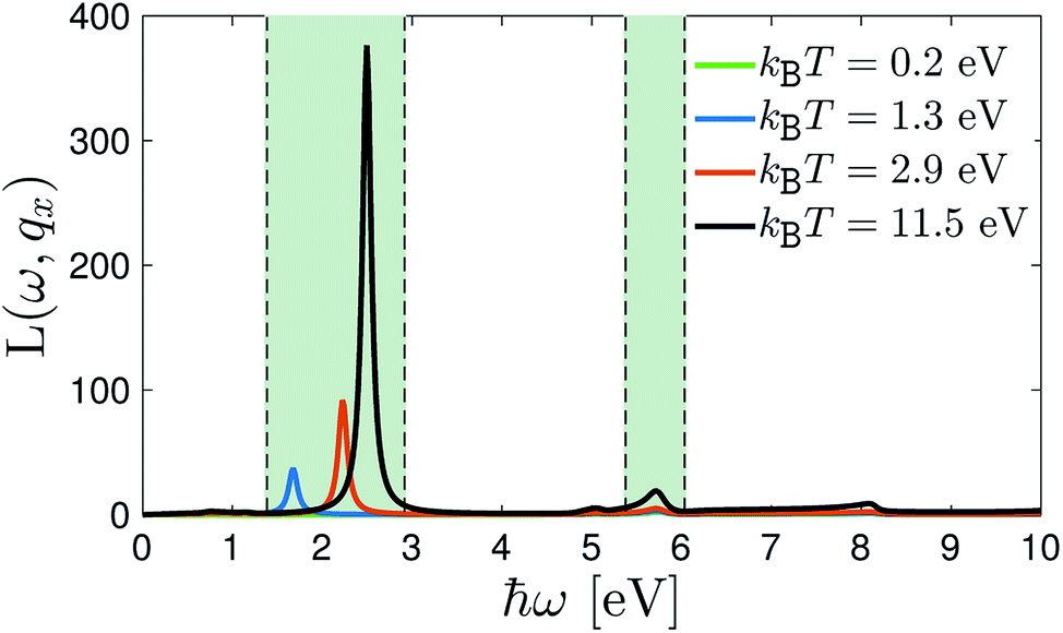 | ||
Fig. 6 The anomalous behavior of the magneto-EELS in two different photon energy ranges with temperature at  and |qxa0| = π/6. and |qxa0| = π/6. | ||
5 Conclusions
In summary, we have obtained the EELS of aBNNRs that were subjected to an external magnetic field and a temperature gradient. Based on the linear response theory and the Green’s function approach, the interplay between σ ↦ σ* or π ↦ π* excitations as well as σ ↦ π* or π ↦ σ* ones with the perturbations above has been explored. The contribution of ribbon width and wave vector transfer has been discussed as well. The analysis depicted that the major impact of the magnetic field on the EELS of the 7-aBNNR manifests itself in the σ ↦ σ* or π ↦ π* excitations for the localized VBM and CBM. Upon increasing the ribbon width, the peak intensities in the EELS were reduced. We found through the EELS curve that a direct-to-indirect band gap transition emerges when the wave vector transfer is perpendicular to the 7-aBNNR plane. Next, we considered a temperature gradient perturbation which was attributed to the modification of kinetic energy and eventually the scattering rate of the carriers. An anomalous behavior for the temperature-dependent EELS in two photon energy transfer ranges was reported. Our results presented here demonstrate a good agreement with the literature, opening a new avenue for extending the nanoplasmonics field to narrower ribbon widths of aNRs in the presence of a magnetic field.Conflicts of interest
There are no conflicts to declare.References
- K. S. Novoselov, A. K. Geim, S. V. Morozov, D. Jiang, Y. Zhang, S. V. Dubonos, I. V. Grigorieva and A. A. Filrsov, Science, 2004, 306, 666–669 CrossRef CAS PubMed.
- K. S. Novoselov, A. K. Geim, S. V. Morozov, D. Jiang, M. I. Katsnelson, I. V. Grigorieva, S. V. Dubonos and A. A. Firsov, Nature, 2005, 438, 197–200 CrossRef CAS PubMed.
- Y. B. Zhang, Y. W. Tan, H. L. Stormer and P. Kim, Nature, 2005, 438, 201–204 CrossRef CAS PubMed.
- C. Berger, Z. M. Song, X. B. Li, X. S. Wu, N. Brown, C. Naud, D. Mayou, t. B. Li, J. Hass, A. N. Marchenkov, E. H. Conrad, P. N. First and W. A. de Heer, Science, 2006, 312, 1191–1196 CrossRef CAS PubMed.
- C. Berger, Z. M. Song, T. B. Li, X. B. Li, A. Y. Ogbazghi, R. Feng, Z. T. Dai, A. N. Marchenkov, E. H. Conrad, P. N. First and W. A. de Heer, J. Phys. Chem. B, 2004, 108, 19912–19916 CrossRef CAS.
- M. Y. Han, B. Ozyilmaz, Y. B. Zhang and P. Kim, Phys. Rev. Lett., 2007, 98, 206805 CrossRef PubMed.
- X. L. Li, X. R. Wang, L. Zhang, S. Lee and H. J. Dai, Science, 2008, 319, 1229–1232 CrossRef CAS PubMed.
- K. Nakada and M. Fujita, Phys. Rev. B, 1996, 54, 17954 CrossRef CAS PubMed.
- Y. Miyamoto, Phys. Rev. B, 1999, 59, 9858 CrossRef CAS.
- H. Lee, Y. W. Son, N. Park, S. Han and J. Yu, Phys. Rev. B, 2005, 72, 174431 CrossRef.
- M. Ezawa, Phys. Rev. B, 2006, 73, 045432 CrossRef.
- Y. W. Son, M. L. Cohen and S. G. Louie, Phys. Rev. Lett., 2006, 97, 216803 CrossRef PubMed.
- V. Barone, O. Hod and G. E. Scuseria, Nano Lett., 2006, 6, 2748–2754 CrossRef CAS PubMed.
- Q. M. Yan, B. Huang, J. Yu, F. W. Zheng, J. Zang, J. Wu, B. L. Gu, F. Liu and W. H. Duan, Nano Lett., 2007, 7, 1469–1473 CrossRef CAS PubMed.
- Z. F. Wang, Q. W. Shi, Q. X. Li, X. P. Wang, J. G. Hou, H. X. Zheng, Y. Yao and J. Chen, Appl. Phys. Lett., 2007, 91, 053109 CrossRef.
- X. J. Wu and X. C. Zeng, Nano Res., 2008, 1, 40–45 CrossRef CAS.
- K. S. Novoselov, D. Jiang, F. Schedin, T. J. Booth, V. V. Khotkevich, S. V. Morozov and A. K. Geim, Proc. Natl. Acad. Sci. U. S. A., 2005, 102, 10451–10453 CrossRef CAS PubMed.
- A. Nag, K. Raidongia, K. P. S. S. Hembram, R. Datta, U. V. Waghmare and C. N. R. Rao, ACS Nano, 2010, 4, 1539–1544 CrossRef CAS PubMed.
- D. Golberg, Y. Bando, Y. Huang, T. Terao, M. Mitome, C. Tang and C. Zhi, ACS Nano, 2010, 4, 2979–2993 CrossRef CAS PubMed.
- M. L. Hu, Z. Z. Yu, K. W. Zhang, L. Z. Sun and J. X. Zhong, J. Phys. Chem. C, 2011, 115, 8260–8264 CrossRef CAS.
- O. V. Yazyev and A. Pasquarello, Phys. Rev. B, 2009, 80, 035408 CrossRef.
- M. Topsakal, E. Aktuerk and S. Ciraci, Phys. Rev. B, 2009, 79, 115442 CrossRef.
- J. Zhou, Q. Wang, Q. Sun and P. Jena, Phys. Rev. B, 2010, 81, 085442 CrossRef.
- N. Yang, C. Xu, J. Hou, Y. Yao, Q. Zhang, M. E. Grami, L. He, N. Wang and X. Qu, RSC Adv., 2016, 6, 18279–18287 RSC.
- T. Huang, X. Zeng, Y. Yao, R. Sun, F. Meng, J. Xu and C. Wong, RSC Adv., 2016, 6, 35847–35854 RSC.
- J. Yu, X. Huang, C. Wu, X. Wu, G. Wang and P. Jiang, Polymer, 2012, 53, 471–480 CrossRef CAS.
- Z. Liu, et al. , Nat. Nanotechnol., 2013, 8, 119–124 CrossRef CAS PubMed.
- C. R. Dean, et al. , Nat. Nanotechnol., 2010, 5, 722–726 CrossRef CAS PubMed.
- M. S. Si, J. Y. Li, H. G. Shi, X. N. Niu and D. S. Xue, Europhys. Lett., 2009, 86, 46002 CrossRef.
- S. Azevedo, J. R. Kaschny, C. M. C. de Castilho and F. de Brito Mota, Eur. Phys. J. B, 2009, 67, 507–512 CrossRef CAS.
- B. Huang and H. Lee, Phys. Rev. B, 2012, 86, 245406 CrossRef.
- N. Berseneva, A. Gulans, A. V. Krasheninnikov and R. M. Nieminen, Phys. Rev. B, 2013, 87, 035404 CrossRef.
- P. Sutter, J. Lahiri, P. Albrecht and E. Sutter, ACS Nano, 2011, 5, 7303–7309 CrossRef CAS PubMed.
- N. Alem, R. Erni, C. Kisielowski, M. D. Rossell, W. Gannett and A. Zettl, Phys. Rev. B, 2009, 80, 155425 CrossRef.
- C. H. Park and S. G. Louie, Nano Lett., 2008, 8, 2200–2203 CrossRef CAS PubMed.
- Z. Zhang and W. Guo, Phys. Rev. B, 2008, 77, 075403 CrossRef.
- K. K. Kim, et al. , Nano Lett., 2012, 12, 161–166 CrossRef PubMed.
- A. Woessner, et al. , Nat. Mater., 2015, 14, 421–425 CrossRef CAS PubMed.
- J. D. Caldwell, et al. , Nat. Commun., 2014, 5, 5221 CrossRef CAS PubMed.
- H. Zeng, C. Zhi, Z. Zhang, X. Wei, X. Wang, W. Guo, Y. Bando and D. Golberg, Nano Lett., 2010, 10, 5049–5055 CrossRef CAS PubMed.
- K. J. Erickson, A. L. Gibb, A. Sinitskii, M. Rousseas, N. Alem, J. M. Tour and A. K. Zettl, Nano Lett., 2011, 11, 3221–3226 CrossRef CAS PubMed.
- W. Chen, Y. Li, G. Yu, C. Z. Li, S. B. Zhang, Z. Zhou and Z. Chen, J. Am. Chem. Soc., 2010, 132, 1699–1705 CrossRef CAS PubMed.
- Y. L. Wang, Y. Ding and J. Ni, Phys. Rev. B, 2010, 81, 193407 CrossRef.
- F. W. Zheng, G. Zhou, Z. R. Liu, J. Wu, W. H. Duan, B. L. Gu and S. B. Zhang, Phys. Rev. B, 2008, 78, 205415 CrossRef.
- J. Qi, X. Qian, L. Qi, J. Feng, D. Shi and J. Li, Nano Lett., 2012, 12, 1224–1228 CrossRef CAS PubMed.
- L. Jin, L. Z. Sun and J. X. Zhong, Chin. Phys. Lett., 2010, 27, 077101 CrossRef.
- J. A. Schuller, E. S. Barnard, W. Cai, Y. C. Jun, J. S. White and M. L. Brongersma, Nat. Mater., 2010, 9, 193–204 CrossRef CAS PubMed.
- E. Verhagen, R. de Waele, L. Kuipers and A. Polman, Phys. Rev. Lett., 2010, 105, 223901 CrossRef PubMed.
- S. Mukherjee, F. Libisch, N. Large, O. Neumann, L. V. Brown, J. Cheng, J. B. Lassiter, E. A. Carter, P. Nordlander and N. J. Halas, Nano Lett., 2013, 13, 240–247 CrossRef CAS PubMed.
- W. H. Hung, M. Aykol, D. Valley, W. Hou and S. B. Cronin, Nano Lett., 2010, 10, 1314–1318 CrossRef CAS PubMed.
- S. Nie and S. R. Emory, Science, 1997, 275, 1102–1106 CrossRef CAS PubMed.
- J. N. Anker, W. P. Hall, O. Lyandres, N. C. Shah, J. Zhao and R. P. V. Duyne, Nat. Mater., 2008, 7, 442–453 CrossRef CAS PubMed.
- J. S. Biteen, D. Pacifici, N. S. Lewis and H. A. Atwater, Nano Lett., 2005, 5, 1768–1773 CrossRef CAS PubMed.
- K. Okamoto, I. Niki, A. Shvartser, Y. Narukawa, T. Mukai and A. Scherer, Nat. Mater., 2004, 3, 601–605 CrossRef CAS PubMed.
- V. E. Ferry, L. A. Sweatlock, D. Pacifici and H. A. Atwater, Nano Lett., 2008, 8, 4391–4397 CrossRef CAS PubMed.
- K. R. Catchpole and A. Polman, Opt. Express, 2008, 16, 21793–21800 CrossRef CAS PubMed.
- J. Fink, M. Knupfer, S. Atzkern and M. S. Golden, J. Electron Spectrosc. Relat. Phenom., 2001, 117, 287–309 CrossRef.
- F. Roth, A. KÃűnig, J. Fink, B. BÃijchner and M. Knupfer, J. Electron Spectrosc. Relat. Phenom., 2014, 195, 85–95 CrossRef CAS.
- H. Ibach and D. L. Mills, Electron Energy Loss Spectroscopy and Surface Vibrations, Academic, New York, 1982 Search PubMed.
- L. Vattuone, L. Savio and M. Rocca, Surface Science Techniques, Springer, Berlin, 2013 Search PubMed.
- R. F. Egerton, Rep. Prog. Phys., 2009, 72, 016502 CrossRef.
- M. K. Kinyanjui, C. Kramberger, T. Pichler, J. C. Meyer, P. Wachsmuth, G. Benner and U. Kaiser, Europhys. Lett., 2012, 97, 57005 CrossRef.
- P. Wachsmuth, R. Hambach, M. K. Kinyanjui, M. Guzzo, G. Benner and U. Kaiser, Phys. Rev. B, 2013, 88, 075433 CrossRef.
- S. C. Liou, C.-S. Shie, C. H. Chen, R. Breitwieser, W. W. Pai, G. Y. Guo and M.-W. Chu, Phys. Rev. B, 2015, 91, 045418 CrossRef.
- J. Hong, K. Li, C. Jin, X. Zhang, Z. Zhang and J. Yuan, Phys. Rev. B, 2016, 93, 075440 CrossRef.
- H. C. Nerl, K. T. Winther, F. S. Hage, K. S. Thygesen, L. Houben, C. Backes, J. N. Coleman, Q. M. Ramasse and V. Nicolosi, npj 2D Materials and Applications, 2017, 1, 2 CrossRef.
- R. Schuster, J. Trinckauf, C. Habenicht, M. Knupfer and B. BÃijchner, Phys. Rev. Lett., 2015, 115, 026404 CrossRef CAS PubMed.
- M. Yarmohammadi, Phys. Rev. B, 2018, 98, 155424 CrossRef CAS.
- J. Wang, F. Ma and M. Sun, RSC Adv., 2017, 7, 16801–16822 RSC.
- K. Zhao, M. Zhao, Z. Wang and Y. Fan, Phys. E, 2010, 43, 440–445 CrossRef CAS.
- B. D. Hoi and M. Yarmohammadi, Europhys. Lett., 2018, 122, 17005 CrossRef.
- H. Zheng, Z. F. Wang, T. Luo, Q. W. Shi and J. Chen, Phys. Rev. B, 2007, 75, 165414 CrossRef.
- G. D. Mahan, Many Particle Physics, Plenum Press, New York, 1993 Search PubMed.
- R. Denk, et al. , Nat. Commun., 2014, 5, 4253 CrossRef CAS PubMed.
- S. Galambosi, et al. , Phys. Rev. B, 2011, 83, 081413 CrossRef.
- C. Tarrio and S. E. Schnatterly, Phys. Rev. B, 1989, 40, 7852 CrossRef CAS PubMed.
- E. Tosatti and F. Bassani, Nuovo Cimento B, 1970, 65, 161–173 CrossRef CAS.
| This journal is © The Royal Society of Chemistry 2019 |