
 Open Access Article
 This Open Access Article is licensed under a Creative Commons Attribution-Non Commercial 3.0 Unported Licence
High-performance thin H:SiON OLED encapsulation layer deposited by PECVD at low temperature
Kyoung Woo Park ab,
Seunghee Leea,
Hyunkoo Leec,
Yong-Hwan Chod,
Yong Cheon Parke,
Sung Gap Ime and
Sang-Hee Ko Park*a
ab,
Seunghee Leea,
Hyunkoo Leec,
Yong-Hwan Chod,
Yong Cheon Parke,
Sung Gap Ime and
Sang-Hee Ko Park*a
aSmart & Soft Materials & Devices Laboratory (SSMD), Department of Materials Science and Engineering, Korea Advanced Institute of Science and Technology (KAIST), 291 Daehak-ro, Yuseong-gu, Daejeon 34141, South Korea. E-mail: shkp@kaist.ac.kr
bModule Development Team, Samsung Display, 1 Samsung-ro, Giheung-gu, Yongin-city, Gyeonggi-do 17113, South Korea
cFlexible Device Research Group, Reality Device Research Division, Electronics and Telecommunications Research Institute (ETRI), 218 Gajeong-ro, Yuseong-gu, Daejeon 34129, South Korea
dDong Woo Fine-Chem, 35, Poseunggongdan-ro 117 Beon-gil, Paseung-eup, Pyeongtaek-si, Gyeonggi-do 17956, South Korea
eFunctional Thin Films Laboratory (FTFL), Department of Chemical and Biomolecular Engineering, Korea Advanced Institute of Science and Technology (KAIST), 291 Daehak-ro, Yuseong-gu, Daejeon 34141, South Korea
First published on 20th December 2018
Abstract
Highly moisture permeation resistive and transparent single layer thin films for the encapsulation of hydrogenated silicon oxynitrides (H:SiON) were deposited by plasma-enhanced chemical vapor deposition (PECVD) using silane (SiH4), nitrous oxide (N2O), ammonia (NH3), and hydrogen (H2) at 100 °C for applications to a top-emission organic light-emitting diode (TEOLED). Addition of H2 into the PECVD process of SiON film deposition afforded the hydrogenated SiON film, which showed not only improved optical properties such as transmittance and reflectance but also better barrier property to water permeation than PECVD SiON and even SiNx. The H:SiON film with thickness of only 80 nm exhibited water vapor transmission rate (WVTR) lower than 5 × 10⁻⁵ g per m2 per day in the test conditions of 38 °C and 100% humidity, where this WVTR is the measurement limit of the MOCON equipment. An additional coating of UV curable polymer enabled the H:SiON films to be flexible and to have very stable barrier property lower than 5 × 10⁻⁵ g per m2 per day even after a number of 10k times bending tests at a curvature radius of 1R. The mild H:SiON film process improved the electrical properties of top-emission OLEDs without generating any dark spots. Furthermore, single H:SiON films having high water vapor barrier could maintain the original illumination features of TEOLED longer than 720 hours. These excellent properties of the H:SiON thin films originated from the structural changes of the SiON material by the introduction of hydrogen.
1 Introduction
Recently, active matrix organic light-emitting diodes (AMOLEDs) have attracted significant attention for applications in not only portable devices but also in large-area transparent displays and TVs. The characteristics of OLEDs such as low weight, flexibility, and self-emitting properties make them suitable for realizing flexible displays.1–3 To realize durable flexible OLED displays, encapsulation technology is critical because OLED displays are extremely vulnerable to degradation by moisture and oxygen.4–6To ensure complete protection of flexible AMOLED displays from water and oxygen, high-performance thin film encapsulation (TFE) with water vapour transmission rate (WVTR) lower than 10−6 g per m2 per day is necessary.7 Moreover, high optical transparency is required because most AMOLEDs used for wearable devices, ultra-high resolution large-area TVs, and transparent displays have top-emission structures. Many studies of TFE on the structure of laminating inorganic and organic layers have been actively carried out because the former and the latter provide excellent barrier properties and flexibility, respectively.8–11 By appropriately laminating the inorganic and organic layers, it is possible to realize excellent TFE that satisfies both requirements of high barrier properties and flexibility.
The laminate structured TFE with inorganic and organic layers, however, has brought about several problems. According to the mechanism for the high barrier properties of the laminated structures, the low permeability of multi-layered structures does not come from the film itself but rather from the interfaces between layers via a delay of water permeability.12 This indicates that an increased number of stacked layers can improve the barrier performance. This complicates the structure of the encapsulation layer with an increase in the thickness of the films. The second problem is the coverage of particles generated during the OLED evaporation process. Only limited materials and deposition methods have been applied to enhance the characteristics of the inorganic barrier layer. Among them, AlOx deposited by the atomic layer deposition (ALD) method is the most representative one for high-performance TFE as it exhibits ultra-thin thickness.13–15 Since the ALD method requires a relatively longer process time than PECVD, AlOx should be relatively much thinner, resulting in poor coverage of particles on OLEDs and degraded encapsulation performance. To solve the above issues, many studies have been attempted to improve the characteristics of the inorganic layer and reduce the number of layers of TFEs.16–18
In this study, by using PECVD at a low temperature of 100 °C or less, we have developed hydrogenated-silicon oxynitride (H:SiON) single layer TFE with high-performance barrier properties. To control the structural characteristics of SiOxNy, a mixture phase of SiOx and SiNxHy was adopted instead of using SiOxNy single phase. The chemical reaction formulas of SiOx, SiNx, and SiOxNy in the PECVD process are shown in (1), (2), and (3).
| SiOx:SiH4 + N2O → SiOx + H2 + N2 | (1) |
| SiNx:SiH4 + NH3 → SiNx + H2 | (2) |
| SiOxNy:SiH4 + N2O + NH3 → SiOxNy + H2 + N2 | (3) |
When hydrogen gas is introduced to the chemical reaction formula (3) with minimized amount of N2O gas, the product can be modified to obtain a new film with hydrogen networks based on SiOxNy. Consequently, high barrier performances can be obtained with a single H:SiON layer.
Furthermore, by coating a single layer of polymer on the H:SiON single layer, we have demonstrated high-performance TFE, which can be applied to OLED and can be used to improve optical characteristics and to ensure good flexibility.
2 Experimental
Based on the SiON single layer structure obtained by the PECVD method, we fabricated TFE with high barrier properties. For good flexibility, a TFE of bi-layered structure was implemented by additional coating of polymer. As a reference film, SiON thin film was deposited on a 50 μm thick PET substrate to a thickness of 80 nm by the PECVD method using SiH4, N2O, and NH3 gases at 100 °C. All the barrier films were deposited on PET (KOLON) with the same thickness. Exceptionally, a 20 μm polyimide (PI) substrate, which was prepared by coating solution PI on the glass substrate followed by thermal curing and laser-lift off, was used in a bending test with a curvature radius of 1R. As can be seen in Table 1, the flow rates of SiH4, N2O, and NH3 gases were 30 sccm, 30 sccm, and 120 sccm, respectively. To realize high-performance barrier property, hydrogen gas was introduced during the deposition to control the characteristics of the SiON thin film. To investigate the effect of hydrogen on the characteristics of the films, hydrogen gas flow rate during the SiON thin film deposition was varied from 0 sccm (film a) to 300 sccm (film b), 500 sccm (film c), and 1000 sccm (film d), and the deposition times of the films were 38, 67, 82, and 112 seconds, respectively. To improve the flexibility, an acrylate-based polymer layer (Dong Woo Fine-Chem) with a thickness of about 1.2 μm was coated on the H:SiON-based layer by the spin-coating method at room temperature. The polymer layer was coated at 1500 RPM for 120 seconds and cured for 60 seconds with UV of 1000 mW at 375 nm wavelength.| SiON | PECVD deposition conditions | ||||
|---|---|---|---|---|---|
| Power (W) | Temperature (°C) | Pressure (torr) | Gas ratio (SiH4![[thin space (1/6-em)]](https://www.rsc.org/images/entities/char_2009.gif) :N2O:NH3:H2, sccm) :N2O:NH3:H2, sccm) |
Thickness (nm) | |
| Film a | 100 | 100 | 1.5 | 30:30:120:0 |
80 |
| Film b | 100 | 100 | 1.5 | 30:30:120:300 |
80 |
| Film c | 100 | 100 | 1.5 | 30:30:120:500 |
80 |
| Film d | 100 | 100 | 1.5 | 30:30:120:1000 |
80 |
To evaluate the barrier property of the TFE layer on top of the OLED, a top-emitting OLED (TEOLED) was fabricated on glass. The glass substrates were sequentially cleaned with acetone and methanol using an ultrasonic bath, followed by rinsing with deionized water. After drying the substrate, a reflective bottom metal, organic materials and a thin top metal layer were deposited in succession using the vacuum thermal evaporation method without breaking the vacuum. During the deposition of the doping layer, the deposition rates of both the host and dopant materials were controlled with a quartz crystal oscillator. To fabricate reference devices, fabricated devices were transferred to an inert environment glove-box, where they were encapsulated using an UV-curable epoxy and a glass cap containing a moisture getter.
To determine the film density and index value, high resolution X-ray diffractometer (SmartLap, RIGAKU) and ellipsometer (ALPHA-SE, J.A. Woollam) were used. Chemical composition was measured by XPS (K-alpha, Thermo VG Scientific). Data were collected after Ar sputtering for 15 seconds in an ultra-high vacuum (base pressure of under 10−9 torr) to remove impurities on the surface of the sample. Fourier Transform Infrared spectroscopy (FT-IR, HYPERION 3000, Bruker) was also conducted with attenuated total reflectance (ATR) mode to analyze the bonding structure of SiON-based thin films. WVTR was measured to be lower than 5 × 10⁻⁵ g per m2 per day (equipment limit at testing sample size of 50 cm2) using Aquatran 2 (MOCON). The water permeability test conditions were 100% in humidity at 38 °C. In addition, optical properties of each sample were examined from 300 nm to 800 nm using UV/VIS/NIR spectrophotometers (SolidSpec-3700, Shimadzu).
The current density–voltage–luminance (J–V–L) characteristics and electroluminescence (EL) spectra of OLEDs were measured using a sourcemeter (Keithley-238, Keithley) and a spectroradiometer (CS-2000, Konica Minolta). All measurements were conducted at room temperature in a dark room. The efficiencies were calculated from the luminance, current density, and EL spectrum.
3 Results and discussion
Characteristics of H:SiON thin films deposited by PECVD method
For the deposition of H:SiON, we set the gas flow rates of SiH4, N2O, and NH3 to be 30, 30, and 120 sccm, respectively, and varied the flow of H2. Fig. 1(a) and (b) show the XRR and XPS analysis results for the thin films with different hydrogen flow rates during thin film deposition. As indicated in Fig. 1(b), the composition ratios of Si, O, and N of film a, film b, film c, and film d were 37.25:61.75:0.99, 37.75:58.09:4.16, 45.25:28.78:25.97, and 49.06:12.87:38.07, respectively. Based on the analysis results, it can be seen that as the hydrogen flow rate increased, the content of hydrogen in the film also increased. It was confirmed from the XRR results as well that the density and index of the thin films increased with increase in hydrogen flow rate. This indicates that hydrogen affects the characteristics and structure of the SiON thin films. These changes can be identified by FT-IR analysis, as shown in Fig. 1(c). While Si–O bonding near 1100 cm−1 decreased, Si–H, Si–N, and N–H bonding near 890 cm−1, 1100 cm−1, and 3375 cm−1 increased or was newly generated by the introduction of hydrogen during the deposition of SiON thin film.
 | ||
| Fig. 1 Analysis results of (a) XRR, (b) XPS, and (c) FT-IR according to hydrogen inflow. | ||
F. Ay et al.20 reported that reducing the N2O gas amount during the SiOxNy film deposition by PECVD using SiH4, N2O, and NH3 resulted in an SiOxNy film with relatively increased N–H bonding due to the influx of hydrogen from NH3. In fact, the original structure of SiON deposited by PECVD can be described as a random bonding model (RBM) structure with a tetrahedral structure of oxide-rich phase. The latter group suggested that the formation of a nitrogen-rich phase resulted in a random mixing model (RMM) structure with tetrahedral and trigonal structures.21 In our case, however, we added additional H2 gas flow while maintaining minimum amount of N2O flow. H2 seems to promote the formation of Si–N–H bonding, leading to a higher index value due to increased stretching vibration of N–H bonding.19,20 Our SiON thin films with increased Si–N–H networking and decreased Si–O seem to suppress the permeation of water vapor due to the increase in film density along with structural changes even in the same amorphous structure. Therefore, during the PECVD process of SiON films, hydrogen plays an important role in improving the index value and growing H:SiON thin films with dense structures.
Water permeability and mechanical bending properties of H:SiON thin films with different hydrogen concentrations
Fig. 2 illustrates the WVTR results of H:SiON films with different amounts of hydrogen incorporation. After 100 hours of testing, the moisture permeability values of film a, film b, film c, and film d were 2.62 × 10⁻¹ g per m2 per day, 3.41 × 10⁻² g per m2 per day, 2.44 × 10⁻³ g per m2 per day, and lower than 5 × 10⁻⁵ g per m2 per day, respectively. In the MOCON measurement tool, WVTR result with negative value indicates that the moisture permeability is less than 5 × 10⁻⁵ g per m2 per day, which is the limitation of the measurement system.18 Although Ca tests can result in WVTR of 10−6 g per m2 per day, the dimension of the sample for the Ca test is mostly less than 4 cm2 and minimizes the probability of introducing particles into the barrier film. Our sample was measured with area of 50 cm2 and 80 nm thickness. These results strongly demonstrate that the moisture permeability of SiON films is improved by hydrogen introduction during thin film deposition. In addition, it has been proven that high moisture barrier property of under 5 × 10⁻⁵ g per m2 per day can be realized with just a 80 nm-thick single thin film layer of H:SiON. These results can be ascribed to changes in the film characteristics such as the density and structure controlled by the incorporation of hydrogen. | ||
| Fig. 2 WVTR results of each H:SiON film with various hydrogen contents. | ||
According to the results of J. Wu et al.,13 multilayer films with 30 nm-thick Al2O3 deposited using the ALD method and 500 nm-thick polymer layers realized WVTR of less than 10−5 g per m2 per day with a total of 3 dyads (6 layers). Considering the process time of ALD, the total thickness of the multi-layered Al2O3 (90 nm) and polymer with total thickness of 1.5 μm and more complicated multi-layered structure, our barrier film has several advantages over these films. For the single SiNx thin film-based TFE deposited by PECVD, the most recent results were published by H. Nominanda et al.18 The results show that a 500 nm SiNx single layer deposited by the PECVD method exhibits WVTR value of less than 5 × 10⁻⁵ g per m2 per day. Considering these recent results, our PECVD processed TFE has advantages in terms of performance and process.
For the potential application of TFE in flexible OLED devices, various evaluations were carried out using film d, which has the best moisture barrier property among various H:SiON films.
Since durability under bending tests is directly related to the lifetime of flexible OLEDs,22,23 it is essential to confirm the mechanical long-term stability of the encapsulation layer. To verify the mechanical properties of film d, we conducted bending tests with various bending radiuses and number of bending times. For the bending test at just 1R bending radius, a 20 μm polyimide substrate was used because 50 μm-thick PET was destroyed in this environment. The barrier property of the single inorganic layer film d was easily degraded after the bending test. To improve the flexibility of this H:SiON film, we coated an acrylate-based polymer on film d by using spin coating, and this was followed by UV curing. Consequently, excellent mechanical reliability was achieved under various bending test conditions, as shown in Fig. 3. Moreover, barrier property lower than 5 × 10⁻⁵ g per m2 per day was maintained in the bi-layered structure of film d with an intact polymer layer even after 10k times bending tests at a radius of curvature of 1R, which is a very harsh condition. This indicates that it is applicable to flexible OLED devices.
 | ||
| Fig. 3 WVTR results after bending test under various conditions. | ||
Optical properties of various structured TFE
We also investigated the effect of polymer films in the bi-layered H:SiON encapsulation film on the optical transmittance and reflectance. Bi-layered H:SiON with polymer film on the PET substrates exhibits transmittance and reflectance of 85.7% and 0.92% (transmittance and reflectance were obtained under wavelengths ranging from 400 nm to 800 nm). As shown in Fig. 4, the transmittance and the reflectance of single film d are 81.4% and 1.43%, respectively. These properties are worse than those of the PET substrate. These negative properties are related to the high index value of film d. However, when film d was laminated with the polymer layer, the transmittance increased to 87.8% and the reflectance decreased to 0.86%. These results can be explained and calculated by Fresnel equations.24,25 In general, the reflection of multi-layered thin films occurs at the interfaces of each layer. Here, the reflected visible lights can be minimized by optimizing the refractive index and the thickness of each thin film, thereby achieving low reflection and increasing the transmittance. | ||
| Fig. 4 Transmittance and reflectance of various structured TFE. | ||
Improvement of the optical properties results in increased luminescence efficiency of OLEDs; therefore, it is a very important requirement for applications to flexible top-emission OLED displays. One peculiar point in the bi-layered structure coated with a polymer layer on film d is the occurrence of wave fluctuation in the visible range. This phenomenon can be due to interference and scattered reflection of light at the interface by defects such as pin-holes in the polymer layer. To clarify the origin of this fluctuation, we introduced iCVD (initiated chemical vapor deposition) processed polymer with similar thickness and less defects compared to the spin-coated polymer. Since the iCVD method is a vacuum coating process, the particle-related defects can be minimized than spin-coating process.26 As shown in Fig. 5, the wave fluctuation is considerably reduced, indicating that both effects result in wave fluctuation. We assume that there is some interference within the double layered barrier film and now, it is under investigation.
 | ||
| Fig. 5 Optical characteristics of bi-layered TFE with the different coating method of the polymer layer. | ||
Comparison of electrical properties of TEOLED encapsulated with single H:SiON film and bi-layered film, and shelf lifetime of TEOLED encapsulated with single H:SiON film
As shown in Fig. 6(a), to evaluate the effect of TFEs on the electrical properties of OLEDs and on the water and oxygen protection properties, we fabricated green-phosphorescent TEOLEDs on the glass substrate. OLEDs comprised aluminum (Al, 100 nm) as an anode/1,4,5,8,9,11-hexaazatriphenylene hexacarbonitrile (HAT-CN, 10 nm) as a hole-injecting layer (HIL)/N,N′-diphenyl-N,N′-bis(1-naphthyl)-1,1′-biphenyl-4,4′′-diamine (NPB, 35 nm) as a hole-transporting layer (HTL)/4,4′,4′-tris(N-carbazolyl)-triphenylamine (TcTa, 10 nm) as an electron-blocking layer (EBL)/2,6-bis(3-(carbazol-9-yl)phenyl)pyridine (26DCzPPy) doped with tris (2-phenylpyridine)iridium(III) (Ir(ppy)3) as the green phosphorescent emitting layer (EML, 7%, 15 nm)/1,3-bis(3,5-dipyrid-3-yl-phenyl)benzene (BmPyPB) as an electron-transporting layer (ETL)/lithium fluoride (LiF, 1 nm) and aluminum (Al, 1.5 nm)/silver (Ag, 25 nm) as an electron-injection layer (EIL) and semi-transparent cathode, respectively, /tris (8-hydroxyquinoline) aluminum (Alq3, 80 nm) as a capping layer. The film d and bi-layered TFE were deposited separately on TEOLEDs.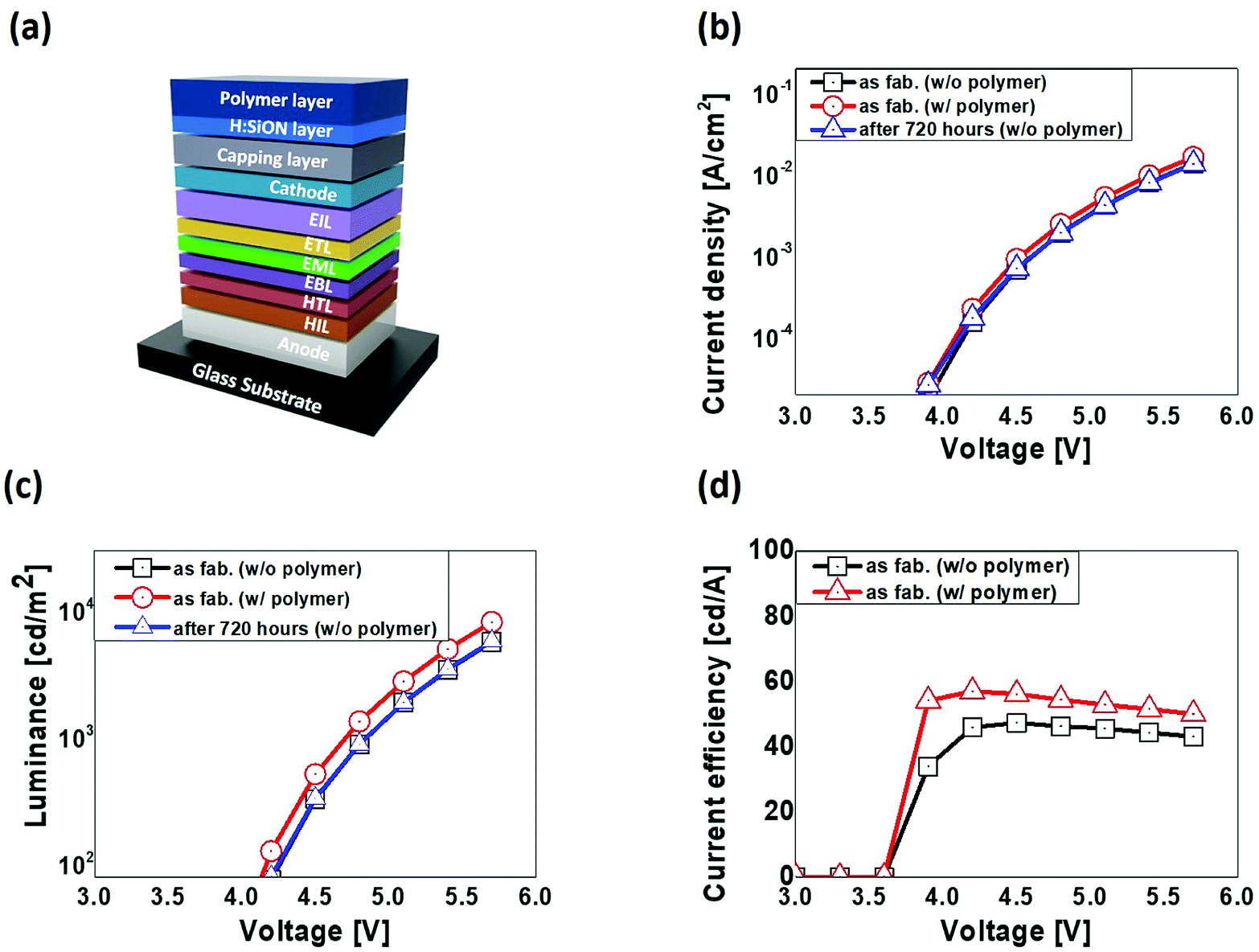 | ||
| Fig. 6 (a) Schematic structure of a TEOLED device fabricated using glass substrate. (b) Current density–voltage, (c) luminance–voltage, and (d) current efficiency curves of TEOLED with various structures and test conditions. | ||
The commercially available flexible AMOLED is typically fabricated on PI of which the coefficient of thermal expansion is less than 7 ppm per °C. Therefore, a substrate barrier film can be deposited at a temperature higher than 300 °C to obtain high barrier property. Here, we focused on OLED thin film encapsulation, which should be deposited under 100 °C. Considering these factors, we fabricated TEOLED on the glass substrate to investigate the electrical and optical characteristics and long-term stability. To compare and evaluate the effect of the encapsulation processes of film d and bi-layered film d with polymer with respect to the TEOLED properties, we measured the electro-optical characteristics of the device such as current density and luminance, as shown in Fig. 6(b) and (c). There were significant differences depending on the addition or non-existence of the polymer layer. The current efficiency values of devices without or with polymer were 45.9 cd A−1 and 56.9 cd A−1, respectively, at 4.2 V. The current efficiency increased by about 16% on average due to the polymer layer. This result, as mentioned above, can be ascribed to the improvement in the optical characteristics of TFE originating from the optical design by Fresnel reflection. As a result, the bi-layered structure coated with a polymer layer on film d not only provides excellent flexibility to TFE but also improves the optical characteristics of TEOLEDs. The operating TEOLED image shown in Fig. 7 also confirms that the TFE process did not induce any kind of damage on the OLED devices.
 | ||
| Fig. 7 Operating images of TEOLEDs (a) without and (b) with a polymer layer, and image (c) after 720 hours shelf lifetime test without the polymer layer. | ||
We carried out a shelf lifetime test for a TEOLED capped with film d at room temperature for 720 hours. The current densities before and after shelf test at 5.7 V were 1.373 × 10⁻² A m−2 and 1.356 × 10⁻² A m−2, and the luminance values were 5746 cd m−2 and 5839 cd m−2, respectively, as shown in Fig. 6(b) and (c). No clear change in electrical properties was observed before and after the shelf lifetime test. However, the generation of dark spots can induce an increase in the current density due to the reduction of the active area of the OLED. Therefore, the operating image of the OLED device should be confirmed. Fig. 7(a) and (c) demonstrate operating images of TEOLEDs before and after 720 hour shelf lifetime test. The device encapsulated with film d showed no clear differences or any dark spots after the shelf lifetime test. Therefore, our TFE provides a high level of protection performance for OLED devices without causing any negative effects.
4. Conclusions
In this study, we have developed a high-performance H:SiON single layer TFE deposited by the PECVD method. To control the characteristics of the SiON thin films, such as the film density and refractive index, hydrogen gas was introduced during the PECVD process. As a result, we obtained new films with different bondings and structures, H:SiON, showing WVTR of lower than 5 × 10⁻⁵ g per m2 per day for an 80 nm-thick film. Moreover, by coating a single polymer layer on H:SiON film, we demonstrated a bi-layer structured high-performance TFE that can be applied to flexible displays with improvement in optical characteristics as well as flexibility. This bi-layered structure exhibited barrier property of lower than 5 × 10⁻⁵ g per m2 per day after 10k times of the bending test at a radius of curvature of 1R. In addition, the optical characteristics were improved by means of index matching, and transmittance and reflectance were 87.8% and 0.86%, respectively. The solution coating process of polymer did not induce any kind of damages such as the generation of dark spots on TEOLED. Finally, we confirmed long-term stability of TEOLED encapsulated with H:SiON through the shelf lifetime test for 720 hours. We observed neither the formation of dark spots nor changes in the electrical performances of the TEOLED, confirming that H:SiON single layer TEF can be a promising solution to high-performance encapsulation for OLEDs including flexible devices.Conflicts of interest
There are no conflicts to declare.Acknowledgements
This work was supported by Wearable Platform Materials Technology Center (WMC) funded by the National Research Foundation of Korea (NRF) Grant of the Korean Government (MSIP) (No. 2016R1A5A1009926).References
- S. Kim, H.-J. Kwon, S. Lee, H. Shim, Y. Chum, W. Choi, J. Kwack, D. Han, M. S. Song, S. Kim, S. Mohammadi, I. S. Kee and S. Y. Lee, Low-Power Flexible Organic Light-Emitting Diode Display Device, Adv. Mater., 2011, 23, 3511–3516 CrossRef CAS PubMed.
- T.-H. Han, Y. Lee, M.-R. Choi, S.-H. Woo, S.-H. Bae, B. H. Hong, J.-H. Ahn and T.-W. Lee, Extremely efficient flexible organic light-emitting diodes with modified graphene anode, Nat. Photonics, 2012, 6, 105–110 CrossRef CAS.
- K.-H. Choi, H.-J. Nam, J.-A. Jeong, S.-W. Cho, H.-K. Kim, J.-W. Kang, D.-G. Kim and W.-J. Cho, High flexible and transparent InZnSnOx/Ag/InZnSnOx multilayer electrode for flexible organic light emitting diodes, Appl. Phys. Lett., 2008, 92, 223302 CrossRef.
- M. Schaer, F. Niiesch, D. Berner, W. Leo and L. Zuppiroli, Water Vapor and Oxygen Degradation Mechanisms in Organic Light Emitting Diodes, Adv. Funct. Mater., 2001, 11(2), 116–121 CrossRef CAS.
- H. Ito, W. Oka, H. Goto and H. Umeda, Plastic Substrates for Flexible Displays, Jpn. J. Appl. Phys., 2006, 45(5), 4325–4329 CrossRef CAS.
- W. Kim, S. Kwon, Y. C. Han, E. Kim, K. C. Choi, S.-H. Kang and B.-C. Park, Reliable Actual Fabric-Based Organic Light-Emitting Diodes: Toward a Wearable Display, Adv. Electron. Mater., 2016, 2, 1600220 CrossRef.
- J. Lewis, Material challenge for flexible organic devices, Mater. Today, 2006, 9(4), 38–45 CrossRef CAS.
- J.-S. Park, H. Chae, H. K. Chung and S. I. Lee, Thin film encapsulation for flexible AM-OLED: a review, Semicond. Sci. Technol., 2011, 26, 034001 CrossRef.
- E. Kim, Y. Han, W. Kim, K. C. Choi, H.-G. Im and B.-S. Bae, Thin film encapsulation for organic light emitting diodes using a multi-barrier composed of MgO prepared by atomic layer deposition and hybrid materials, Org. Electron., 2013, 14, 1737–1743 CrossRef CAS.
- J. Meyer, P. Gorrn, F. Bertram, S. Hamwi, T. Winkler, H.-H. Johannes, T. Weimann, P. Hinze, T. Riedl and W. Kowalsky, Al2O3/ZrO2 Nanolaminates as Ultrahigh Gas-Diffusion Barriers – A Strategy for Reliable Encapsulation of Organic Electronics, Adv. Mater., 2009, 21, 1845–1849 CrossRef CAS.
- J. H. Kwon, Y. Jeon, S. Choi, H. Kim and K. C. Choi, Synergistic gas diffusion multilayer architecture based on the nanolaminate and inorganic-organic hybrid organic layer, J. Inf. Disp., 2018, 19(3), 135–142 CrossRef CAS.
- G. L. Graff, R. E. Williford and P. E. Burrows, Mechanisms of vafor permeation through multilayer barrier films: lag time versus equilibrium permeation, J. Appl. Phys., 2004, 96(4), 1840–1849 CrossRef CAS.
- J. Wu, F. Fei, C. Wei, X. Chen, S. Nie, D. Zhang, W. Su and Z. Cui, Efficient multi-barrier thin film encapsulation of OLED using alternating Al2O3 and polymer layers, RSC Adv., 2018, 8, 5721–5727 RSC.
- M. D. Groner, S. M. George, R. S. McLean and P. F. Carcia, Gas diffusion barriers on polymers using Al2O3 atomic layer deposition, Appl. Phys. Lett., 2006, 88, 051907 CrossRef.
- P. F. Carcia, R. S. McLean, M. D. Groner, A. A. Dameron and S. M. George, Gas diffusion ultrabarriers on polymer substates using Al2O3 atomic layer deposition and SiN plasma-enhanced chemical vapor deposition, J. Appl. Phys., 2009, 106, 023533 CrossRef.
- S.-H. K. Park, J. Oh, C.-S. Hwang, J.-I. Lee, Y. S. Yang and H. Y. Chu, Ultrathin Film Encapsulation of an OLED by ALD, Electrochem. Solid-State Lett., 2005, 8(2), H21–H23 CrossRef CAS.
- P. V. Weijer, P. C. P. Bouten, S. Unnikrishnan, H. B. Akkerman, J. J. Michels and T. M. B. Mol, High-performance thin-film encapsulation for organic light-emitting diodes, Org. Electron., 2017, 44, 94–98 CrossRef.
- H. Nominanda, W. Wu, J. R. Chen and S. Y. Choi, Large Area Thin Film Encapsulation from Bendable to Rollable and Foldable, Dig. Tech. Pap.–Soc. Inf. Disp. Int. Symp., 2018, 82–1, 1103–1105 CrossRef.
- W. A. P. Claassen, W. G. J. N. Valkenburg, F. H. P. M. Habraken and Y. Tamminga, Characterization of Plasma Silicon Nitride Layers, J. Electrochem. Soc., 1983, 130(12), 2419–2423 CrossRef CAS.
- F. Ay and A. Aydinli, Comparative investigation of hydrogen bonding in silicon based PEVCD grown dielectrics for optical waveguides, Opt. Mater., 2004, 26, 33–46 CrossRef CAS.
- V. G. Caranasi, A. Ilyas, M. F. Velten, A. Shah, W. A. Lanford and P. B. Aswath, Role of Hydrogen and Nitrogen on the surface Chemical Structure of Bioactive Amorphous Silicon Oxynitride Films, J. Phys. Chem. B, 2017, 121, 8991–9005 CrossRef PubMed.
- D.-U. Jin, J.-S. Lee, T.-W. Kim, S.-G. An, D. Straykhilev, Y.-S. Pyo, H.-S. Kim, D.-B. Lee, Y.-G. Mo, H.-D. Kim, and H.-K. Chung, World-Largest(6.5”) Flexible Full Color Top Emission AMOLED Display on Plastic Film And Its Bending Properties, SID DIGEST, 2009, pp. 983–985 Search PubMed.
- N. Kim and S. Graham, Development of highly flexible and ultra-low permeation rate thin-film barrier structure for organic electronics, Thin Solid Films, 2013, 547, 57–62 CrossRef CAS.
- F. W. Mont, J. K. Kim, M. F. Schubert, E. F. Schubert and R. W. Siegel, High-refractive-index TiO2-nanoparticle-loaded encapsulants for light-emitting diodes, J. Appl. Phys., 2008, 103, 083120 CrossRef.
- M. Ma, F. W. Mont, X. Yan, J. Cho, E. F. Schubert, G. B. Kim and C. Sone, Effect of the refractive index of the encapsulant on the light-extraction efficiency of light-emitting diodes, Opt. Express, 2011, 19(S5), A1135–A1140 CrossRef CAS PubMed.
- B. J. Kim, H. K. Park, H. J. Seong, M. S. Lee, B.-H. Kwon, D. H. Kim, Y. I. Lee, H. K. Lee, J.-I. Lee and S. G. Im, A Single-Chamber System of Initiated Chemical Vapor Deposition and Atomic Layer Deposition for Fabrication of Organic/Inorganic Multilayer Films, Adv. Eng. Mater., 2017, 19(6), 1600819 CrossRef.
| This journal is © The Royal Society of Chemistry 2019 |