
 Open Access Article
 This Open Access Article is licensed under a Creative Commons Attribution-Non Commercial 3.0 Unported Licence
Facile organic surfactant removal of various dimensionality nanomaterials using low-temperature photochemical treatment†
Chahwan Hwang‡
a,
Jae Sang Heo‡bc,
Kyung-Tae Kimb,
Yeo Kyung Kanga,
Byungdoo Choia,
Yong-Hoon Kim d,
Antonio Facchettief,
Sung Kyu Park*b and
Myung-Gil Kim*a
d,
Antonio Facchettief,
Sung Kyu Park*b and
Myung-Gil Kim*a
aDepartment of Chemistry, Chung-Ang University, Seoul 06980, Korea. E-mail: myunggil@cau.ac.kr
bSchool of Electrical and Electronics Engineering, Chung-Ang University, Seoul 06980, Korea. E-mail: skpark@cau.ac.kr
cDepartment of Medicine, University of Connecticut Health Center, Farmington, CT 06030, USA
dSKKU Advanced Institute of Nanotechnology (SAINT), School of Advanced Materials Science and Engineering, Sungkyunkwan University, Suwon 16419, Korea
eDepartment of Chemistry, The Materials Research Center, Northwestern University, 2145 Sheridan Road, Evanston, Illinois 60208, USA
fFlexterra Corporation, 8025 Lamon Avenue, Skokie, Illinois 60077, USA
First published on 4th January 2019
Abstract
Deep ultraviolet (DUV)-treatment is an efficient method for the removal of high-energy-barrier polymeric or aliphatic organic ligands from nanomaterials. Regardless of morphology and material, the treatment can be used for nanoparticles, nanowires, and even nanosheets. The high-energy photon irradiation from low-pressure mercury lamps or radio frequency (RF) discharge excimer lamps could enhance the electrical conductivity of various nanomaterial matrixes, such as Ag nanoparticles, Bi2Se3 nanosheets, and Ag nanowires, with the aliphatic alkyl chained ligand (oleylamine; OAm) and polymeric ligand (polyvinyl pyrrolidone; PVP) as surfactants. In particular, Ag nanoparticles (AgNPs) that are DUV-treated with polyvinyl pyrrolidone (PVP) for 90 min (50–60 °C) exhibited a sheet resistance of 0.54 Ω □−1, while thermal-treated AgNP with PVP had a sheet resistance of 7.5 kΩ □−1 at 60 °C. The simple photochemical treatment on various dimensionality nanomaterials will be an efficient sintering method for flexible devices and wearable devices with solution-processed nanomaterials.
Introduction
Solution-processed electronics are able to achieve high throughput, material efficiency, and cost-effective fabrication for next-generation large area electronics, such as flexible displays, wearable devices, and electronic skins.1–6 Novel materials and innovative processing methods have been investigated for their applicability as low-temperature solution-processed electronic devices with high electrical performance and unprecedented functionalities.7,8 For example, the variety of chemical groups in organic semiconductors enables the simple control of chemical properties for solution processing and good electrical performance.9,10 Moreover, there have been significant efforts on newly emerging inorganic materials, such as sol–gel oxide precursors, soluble metal halide perovskite, nanomaterials, and polymeric silicon precursors, which provide soluble materials or precursors with intrinsically high electrical performances.11–14 In particular, soluble inorganic nanomaterials exhibited promising electronic functionalities, which include high electrical conductivity with optical transparency, high carrier mobility, high optical absorption, or chemical sensing abilities.15,16 The well-developed chemical synthetic strategies of nanomaterials enabled finely tuned electronic materials for each target application, which surpasses even the corresponding bulk material properties.17,18The incorporation of organic ligands, such as polyvinyl pyrrolidone (PVP), oleylamine (OAm), oleic acid (OA), and polyamidoamine (PAMAM), is important to achieving highly soluble nanomaterials.19–21 Although the use of organic ligands as a surfactant could stabilize high-energy surfaces and prevent the aggregation of nanomaterials,20 the long-chain organic ligands on nanomaterial surfaces can act as highly electric insulating barriers between nanomaterials, which results in the poor electrical connection of nanomaterials and significant electrical performance degradation.22 To improve the electrical performance of nanomaterial networks, the removal of organic ligands is a crucial step for the intimate contact formation between nanomaterials and subsequent fast-charge transport in nanomaterial matrixes. Until now, several strategies have been developed to remove the organic ligands with insulating characteristics using thermal annealing, UV-ozone (UVO) treatment, or the ligand-exchange method.22–24 Of these strategies, high-temperature thermal annealing under inert, oxidative, or reductive atmospheres has been widely employed as a simple and effective method.23,24 Unfortunately, the thermal annealing method results in undesirable morphological changes, such as grain growth and the destruction of anisotropic shapes, the loss of the quantum confinement effect, and electric disconnection.25,26 Moreover, high-temperature treatment is incompatible with flexible plastic substrates such as polyethylene terephthalate (PET).27 In the case of UVO treatment, the low thermal budget ligand removal is possible with high oxidative O3 generation. Although O3 could easily oxidize and remove organic ligands, undesirable oxidation on nanomaterial surfaces results in significant electrical performance degradation.28 Unlike thermal annealing and UVO treatment, the ligand-exchange strategy can convert long alkyl chains on nanomaterials to short organic molecules that can be easily removed with mild heating or low-temperature vacuum treatment.29–31 However, the ligand-exchange method is only applicable for alkyl chained-ligands with relatively low binding strengths on nanomaterials. In addition, there is organic acid treatment or hydrazine treatment for the cleaning of nanomaterial surfaces, which generally induces the aggregation of nanomaterials or produces potentially hazardous waste.32,33
For organic and inorganic materials, there is a significant contrast in terms of their photochemical stabilities.34,35 While the weak covalent bonding in organic molecules can be destructed by high-intensity deep ultraviolet (DUV) light irradiation, relatively stable inorganic materials with extended structures usually remain intact, even after high-dose DUV irradiation.36 For example, high-quality metal oxide semiconductor (MOS) films and well-defined organic semiconductor films were successfully demonstrated by using photochemical annealing and photochemical patterning, respectively.34,35 Considering the photochemical stability difference between organic ligands and inorganic nanomaterials, the simple DUV irradiation could successfully achieve organic surfactant removal on inorganic nanomaterials, and enhance the charge transport between nanomaterials.
In this study, we report that the simple photochemical DUV-treatment on solution-processed nanomaterial matrixes achieved facile removal of organic surfactants and significant charge-transport enhancement between nanomaterials. To compare the thermal annealing method and DUV treatment at low temperature, two types of ligands on Ag nanoparticles (AgNPs), namely the aliphatic alkyl chained ligand (oleylamine; OAm) and polymeric ligand (polyvinyl pyrrolidone; PVP), were used as surfactants. The DUV treatment for these materials showed reasonable or even superior electrical performance compared with the thermal annealing method without any change of shape and aggregation. Furthermore, we investigated the effect of low-temperature photochemical treatment for various dimensional conducting nanomaterials such as Bi2Se3 nanosheets (NSs), and Ag nanowires (NWs). Overall, the DUV treatment could be employed as a general strategy for the low-temperature electrical activation of nanomaterials for next-generation low-cost large-area electronics.
Experimental
Nanomaterial synthesis
![[thin space (1/6-em)]](https://www.rsc.org/images/entities/char_2009.gif) 000) was dissolved in 200 ml of ethyleneglycol (EG), after which 6 ml of NiCl2 (1 mM in EG) solution was added as a seed molecule above the solution with stirring at 400 rpm. After the reaction temperature of the solution was increased to 170 °C, 5.1 g of AgNO3 solution (10 wt% in EG) was added dropwise into the solution. The reaction was completed after 1 h, and the solution was cooled to room temperature. Then, 600 ml of acetone was added to the solution to precipitate the AgNWs, after which the supernatant was decanted. The precipitates were dispersed in 50 ml of isopropyl alcohol (IPA), and then the dispersion was centrifuged at 4000 rpm for 3 min. The process was repeated 3 times. Finally, the AgNWs were dispersed in IPA for 0.5 wt% prior to spray coating.000) was dissolved in 400 ml of ethyleneglycol. The solution temperature was increased to 80 °C. After the dissolution of all reagents, 3 ml of formic acid (85%) was slowly dropped into the solution, and then the solution was further stirred for 12 h. The solution was cooled, and 1200 ml of acetone was added to the solution to precipitate the AgNPs. After the AgNPs completely precipitated, the supernatant was decanted. Then, 100 ml of hot de-ionized water/IPA (1:1) solution was added to the precipitates and sonicated for 30 min to fully dispersed AgNPs. Next, 300 ml of acetone was added to the dispersion, and it was then centrifuged at 5000 rpm for 3 min. The process was repeated 5 times. Finally, the PVP-AgNPs were dispersed in IPA for 25 wt% with sonication.000) were dissolved in 150 ml of ethyleneglycol. Then, the solution was refluxed at 190 °C for 6 h with stirring. After the reaction was finished, the black solution was cooled to room temperature, and 300 ml of acetone was added to the solution to obtain Bi2Se3 precipitates. The precipitates were redispersed with 40 ml of IPA, and then centrifuged at 8000 rpm for 7 min. The process was then repeated 3 times to remove the impurities. After final centrifugation, Bi2Se3 NSs were redispersed with 10 ml of IPA. The Bi2Se3 NSs dispersion was centrifuged at 3000 rpm for 3 min prior to spray coating, and then the supernatant was used for the spray coating solution.
000) was dissolved in 200 ml of ethyleneglycol (EG), after which 6 ml of NiCl2 (1 mM in EG) solution was added as a seed molecule above the solution with stirring at 400 rpm. After the reaction temperature of the solution was increased to 170 °C, 5.1 g of AgNO3 solution (10 wt% in EG) was added dropwise into the solution. The reaction was completed after 1 h, and the solution was cooled to room temperature. Then, 600 ml of acetone was added to the solution to precipitate the AgNWs, after which the supernatant was decanted. The precipitates were dispersed in 50 ml of isopropyl alcohol (IPA), and then the dispersion was centrifuged at 4000 rpm for 3 min. The process was repeated 3 times. Finally, the AgNWs were dispersed in IPA for 0.5 wt% prior to spray coating.000) was dissolved in 400 ml of ethyleneglycol. The solution temperature was increased to 80 °C. After the dissolution of all reagents, 3 ml of formic acid (85%) was slowly dropped into the solution, and then the solution was further stirred for 12 h. The solution was cooled, and 1200 ml of acetone was added to the solution to precipitate the AgNPs. After the AgNPs completely precipitated, the supernatant was decanted. Then, 100 ml of hot de-ionized water/IPA (1:1) solution was added to the precipitates and sonicated for 30 min to fully dispersed AgNPs. Next, 300 ml of acetone was added to the dispersion, and it was then centrifuged at 5000 rpm for 3 min. The process was repeated 5 times. Finally, the PVP-AgNPs were dispersed in IPA for 25 wt% with sonication.000) were dissolved in 150 ml of ethyleneglycol. Then, the solution was refluxed at 190 °C for 6 h with stirring. After the reaction was finished, the black solution was cooled to room temperature, and 300 ml of acetone was added to the solution to obtain Bi2Se3 precipitates. The precipitates were redispersed with 40 ml of IPA, and then centrifuged at 8000 rpm for 7 min. The process was then repeated 3 times to remove the impurities. After final centrifugation, Bi2Se3 NSs were redispersed with 10 ml of IPA. The Bi2Se3 NSs dispersion was centrifuged at 3000 rpm for 3 min prior to spray coating, and then the supernatant was used for the spray coating solution.Film deposition and characterization
Results and discussion
Fig. 1 schematically describes the photochemical removal process of organic ligands and the fabrication of conducting electrodes with nanomaterials. As shown in Fig. 1a, the nanomaterial conductors initially have a poor electrical connection between spatially separated nanomaterials with organic ligands on nanomaterial surfaces, regardless of the dimension or morphology of the nanomaterials, such as NPs, NWs, and NSs. Generally, the insulating organic ligands with a high-energy barrier hinder the carrier movement and simultaneously decrease the electrical conductivity of nanomaterial arrays. Therefore, it is essential that these insulating ligands should be removed using effective methods to form a carrier-transport pathway between nanomaterials. As shown in Fig. 1b, we expected that successful removal of the organic ligands on metal nanomaterials via photochemical activation (DUV or excimer treatment; 254 nm/185 nm or 172 nm) can lead to the bond breaking of organic surfactants with a sufficiently high photon energy and the easy percolation of free charge carriers between nanomaterials. Consequently, the photochemically treated nanomaterials could achieve higher electrical conductivity than nanomaterials without photochemical activation owing to the clean removal of insulating ligands on nanomaterials. In order to investigate the efficiency of photochemical treatment for the removal of organic ligands, we used two different types of ligand (OAm and PVP) capped AgNPs, and three types of morphology (0D, 1D, 2D) which correspond to PVP- or OAm-AgNPs, PVP-AgNWs, and PVP-Bi2Se3 NSs, respectively.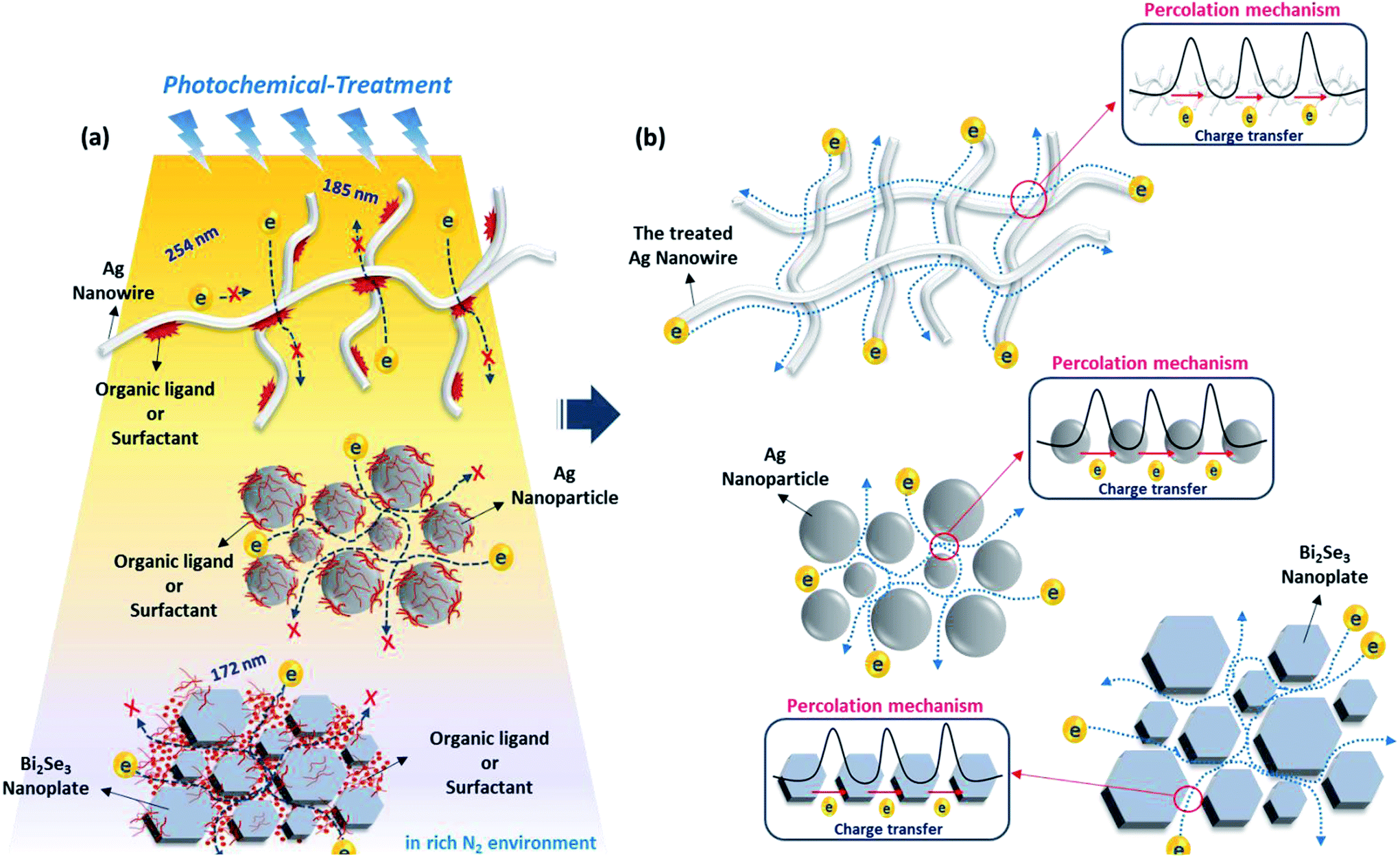 | ||
| Fig. 1 Experimental scheme for photochemical activation on various dimensional metal or metal–chalcogenide nanomaterials. (a) Concept for photochemical activation and removal of organic ligands on nanomaterials. (b) Percolation mechanism of various morphology nanomaterials by photochemical activation. | ||
Fig. 2 shows the sheet resistances of nanomaterials (AgNPs, AgNWs, Bi2Se3 NSs) with thermal and DUV-treatment. In the case of the AgNPs, aliphatic oleylamine (OAm) and polymeric polyvinylpyrrolidone (PVP) ligands were used as surfactants. The initial nanomaterials showed poor electrical conductivities with few available electrical contacts between nanomaterials or impurity mediated conduction.41 As shown in Fig. 2a and c, although the initial conductive characteristics were different, the sheet resistances of AgNP films with OAm and PVP decreased according to the increase of the annealing temperature (30 min). The thermal annealing induces the shrinkage, vaporization, or partial decomposition of polymeric or hydrocarbon chains, which make the surfaces of each AgNP have closer contact. Furthermore, the AgNPs that in contact were sintered at the specific temperature because of the lower melting point of small AgNPs with high surface energy. However, a relatively high temperature (above 200 °C) is still needed to achieve higher conductivity values that are similar to that of bulk silver, so thermal annealing treatment is not suitable for the fabrication of conducting electrodes on cheap plastic substrates, such as PET film. Compared to thermal annealing treatment, DUV treatment significantly decreased the sheet resistance of AgNPs at low temperatures of 50–60 °C. In particular, the DUV treatment of AgNPs with PVP for 30 min (50–60 °C) resulted in a sheet resistance of 4.45 Ω □−1, while the thermal-treatment of AgNPs with PVP resulted in a sheet resistance of 7.5 kΩ □−1 at a similar annealing temperature of 60 °C. The further DUV irradiation for 90 min on AgNPs with PVP resulted in a very low sheet resistance of 0.54 Ω □−1 without film morphology degradation. This result indicates that the DUV treatment process induces a dramatic reduction in the sheet resistance of AgNP films at low temperature owing to the effective cleavage or removal of organic ligands on AgNP materials.34,35
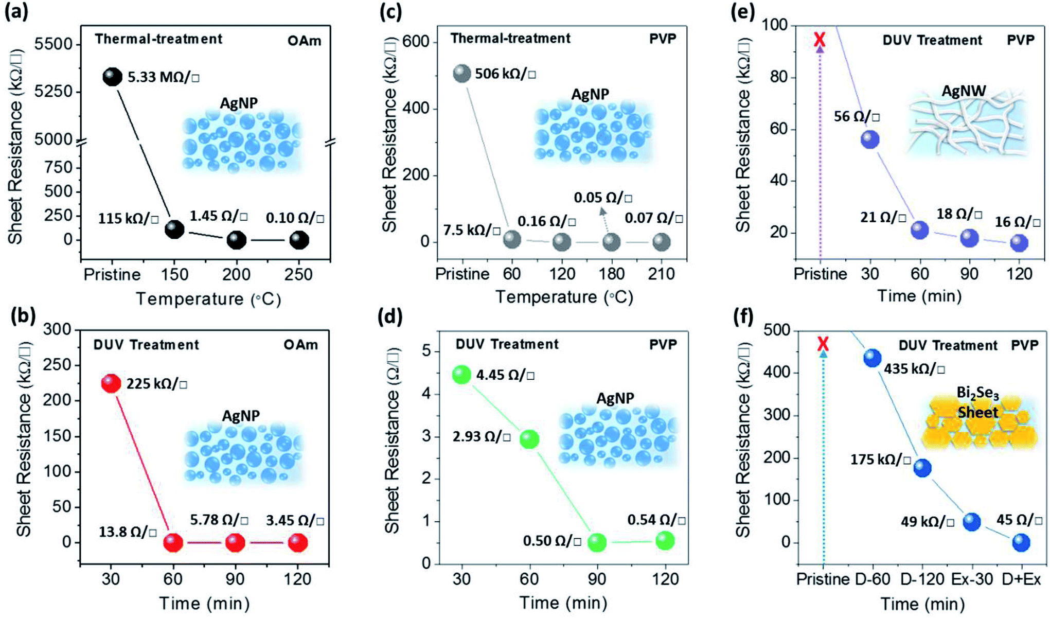 | ||
| Fig. 2 Electrical characteristics of metal or metal–chalcogenide nanomaterials (AgNPs, AgNWs, and Bi2Se3 NSs). (a) Sheet resistance of OAm-AgNPs by thermal treatment at R.T., 150, 200, and 250 °C. (b) Sheet resistance of OAm-AgNPs by DUV treatment for 30, 60, 90, 120 min. (c) Sheet resistance of PVP-AgNPs by thermal treatment at R.T., 60, 120, 180 and 210 °C. (d) Sheet resistance of PVP-AgNPs by DUV treatment for 30, 60, 90, 120 min. (e) Sheet resistance of PVP-AgNWs by DUV treatment for 30, 60, 90, 120 min. (f) Sheet resistance of PVP-Bi2Se3 NSs by DUV treatment for 60, 120 min, excimer only for 30 min, and DUV 30 min + excimer 30 min. | ||
To demonstrate the generality of photochemical treatment for low-temperature nanomaterial conductor fabrication, nanomaterials having various shapes, such as PVP-AgNWs and PVP-Bi2Se3 NSs films, were exposed to DUV and excimer (172 nm) irradiations. The PVP-AgNW film exhibited a similar tendency as that of PVP-AgNP films for DUV treatment. The resistance of PVP-AgNW films reduced up to 16 Ω □−1 as the DUV exposure time increased (Fig. 2e). In comparison, the thermally treated AgNW films showed improved sheet resistance of 25.7 Ω □−1 after high temperature annealing at 150 °C (ESI Fig. S1a†). However, PVP-Bi2Se3 NS films could not achieve high conductivity close to the bulk characteristic using only DUV treatment, unlike PVP-AgNP or PVP-AgNW films. Without excimer treatment, the sheet resistances of PVP-Bi2Se3 NS films with DUV-60 min and DUV-120 min had values of 435 kΩ □−1 and 175 kΩ □−1, respectively. The sheet-shape of PVP-Bi2Se3 NSs may reflect electromagnetic wave and hinder its pathway through the stacked-structure. The confined nature of organic ligands between Bi2Se3 NSs resulted the significant increase of thermal treatment temperature of the NS films upto 300 °C for reasonable sheet resistance of 473 Ω □−1 (ESI Fig. S1b†). In contrast, shorter wavelength-excimer treatment (30 min) can lead to the enhancement of the conductivity of PVP-Bi2Se3 NS films (49 kΩ □−1). In the case where both DUV and excimer were sequentially treated in a short time, the PVP on Bi2Se3 NSs was effectively removed. In our preliminary test, a long irradiation time of the excimer (>30 min) with high-intensity energy enables the removal of the organic ligands, and influences the structural integrity of PVP-Bi2Se3 NS, resulting in the degradation of the electrical performance. As shown in Fig. 2f, the sheet resistance of PVP-Bi2Se3 the NS film significantly decreased to 45 Ω □−1 by the successive photochemical activation with two different values of photo-energy (DUV and excimer). Consequently, it indicated that photochemical activation is effectively capable of removing the insulating organic ligands on the surface of nanomaterials without any thermal treatment, regardless of the shape or structure of nanomaterials.
In order to investigate the variation of the OAm-AgNPs surface morphology with or without thermal or DUV treatment, field-emission scanning electron microscopy (FE-SEM) images were obtained, as shown in Fig. 3a–d. The pristine sample (Fig. 3a) showed that a large amount of OAm ligand is present within the large size of AgNPs and OAm aggregates. After thermal (<150 °C) or DUV treatment, the OAm ligand aggregates on the top surface of AgNPs were removed, and the original grain of AgNPs was revealed owing mainly to OAm slow evaporation, as shown in Fig. 3c, d and S2 (ESI†). However, the grains of OAm-AgNPs grew and aggregated above a specific annealing temperature (>150 °C) owing to the filling of the empty space during the OAm evaporation and sintering (Fig. 3b).42 This aggregation phenomenon shifted toward the side edge of the substrate, which resulted in the generation of a charge-carrier transport pathway at the only side edge, as shown in Fig. S3 (ESI†). On the contrary, with the increased irradiation time of DUV treatment, there was no significant variation of the size or shape and aggregation of AgNPs. The DUV treatment induced the slight growth of the particle size with an increasing DUV irradiation time because the partial nano-welding between particles that were in close contact was due to the plasmon effect (Fig. S4 in ESI†).43,44 Consequently, the FE-SEM images showed that the photochemical treatment is an effective process for the removal of OAm ligands on AgNPs without any deformation or degradation of AgNPs in spite of the long irradiation time at low temperature. To confirm the OAm ligand removal on AgNP surfaces using DUV treatment, we have implemented Raman spectroscopy analysis for OAm-capped AgNP films with different DUV irradiation times, as shown in Fig. 3f. The OAm ligand peak is located at wavenumbers of 1200–1400 cm−1 of the C–H bending mode, and 1600–1800 cm−1 of C![[double bond, length as m-dash]](https://www.rsc.org/images/entities/char_e001.gif) C stretching and N–H bending mode.45 Raman spectra in Fig. 3f showed that the OAm ligand on AgNPs was gradually removed as the DUV irradiation time increased. However, in the case of the thermal treatment, the intensity peak corresponding to the OAm ligand was increased at an annealing temperature of >150 °C, as shown in Fig. 3e. It can be considered that molten OAm molecules spontaneously desorbed on the NPs and moved to the top of the NP films or empty space formed by sintered NPs. Further, the remaining OAm cannot be easily removed owing to its high boiling point (>300 °C). Consequently, the OAm ligand can be easily removed by DUV treatment at low temperature without a specific change in the AgNP shapes and the generation of undesirable products, resulting in a significant improvement of the electrical performances.
C stretching and N–H bending mode.45 Raman spectra in Fig. 3f showed that the OAm ligand on AgNPs was gradually removed as the DUV irradiation time increased. However, in the case of the thermal treatment, the intensity peak corresponding to the OAm ligand was increased at an annealing temperature of >150 °C, as shown in Fig. 3e. It can be considered that molten OAm molecules spontaneously desorbed on the NPs and moved to the top of the NP films or empty space formed by sintered NPs. Further, the remaining OAm cannot be easily removed owing to its high boiling point (>300 °C). Consequently, the OAm ligand can be easily removed by DUV treatment at low temperature without a specific change in the AgNP shapes and the generation of undesirable products, resulting in a significant improvement of the electrical performances.
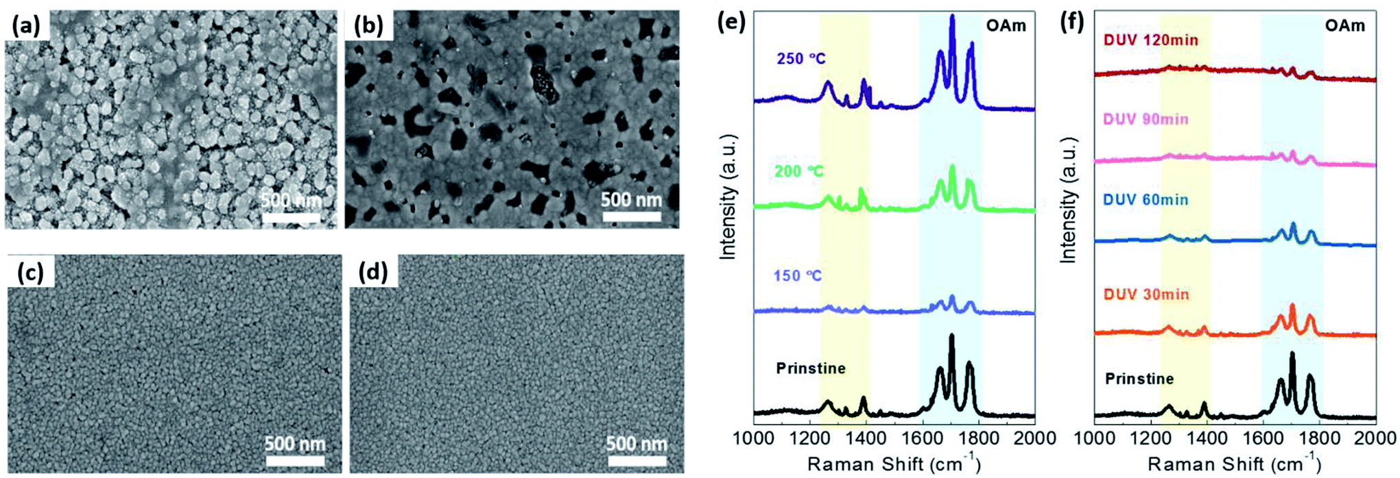 | ||
| Fig. 3 Morphology (FE-SEM) and chemical analysis (Raman) of the OAm-AgNPs with DUV and thermal treatment. (a and b) FESEM image of (a) pristine OAm-AgNPs, and (b) thermal annealed OAm-AgNPs at 200 °C. (c and d) FESEM image of DUV treated OAm-AgNPs for (c) 60 min and (d) 90 min. (e and f) Raman spectrum variation of OAm-AgNP films obtained using (e) thermal and (f) DUV treatment. | ||
In the case of PVP-AgNPs, (Fig. 4a–d), the decrease in the distance between AgNPs and the increase in the AgNP size were accompanied by the PVP ligand removal and the partial nano-welding via DUV treatment, while the thermal-treated PVP-AgNPs were aggregated by partial sintering at an annealing temperature greater than 120 °C (Fig. S5 in the ESI†). As with OAm-AgNPs, thermally treated PVP-AgNPs exhibited large grain growth above 180 °C (Fig. 4b), as well as the subsequent formation of many voids owing to film shrinkage. Fig. 4e and f show the Raman spectra of thermal and DUV treatment for AgNPs with PVP ligands, respectively. As the annealing temperature and DUV irradiation time increased, the peak at 2935 cm−1 of the C–H stretching mode corresponding to PVP ligands markedly decreased.46 Because DUV treatment enabled the degradation of the C–H, CO, even the C–C bond by sigma–sigma* or pi–pi* transition, a polymeric hydrocarbon chain was converted into short and volatile components that will be easily evaporated into the atmosphere. Therefore, the percolation conduction of AgNPs with PVP ligands could be improved by removing the potential barrier of organic ligands on metal nanomaterials using photochemical activation, resulting in enhanced charge-carrier transfer between nanomaterials. The facile removal of organic ligands with photochemical treatment could be further implemented for the fabrication of various solution-processed electronic devices with nanomaterials, such as thin-film transistors, solar cells, light emitting diodes, and sensors.
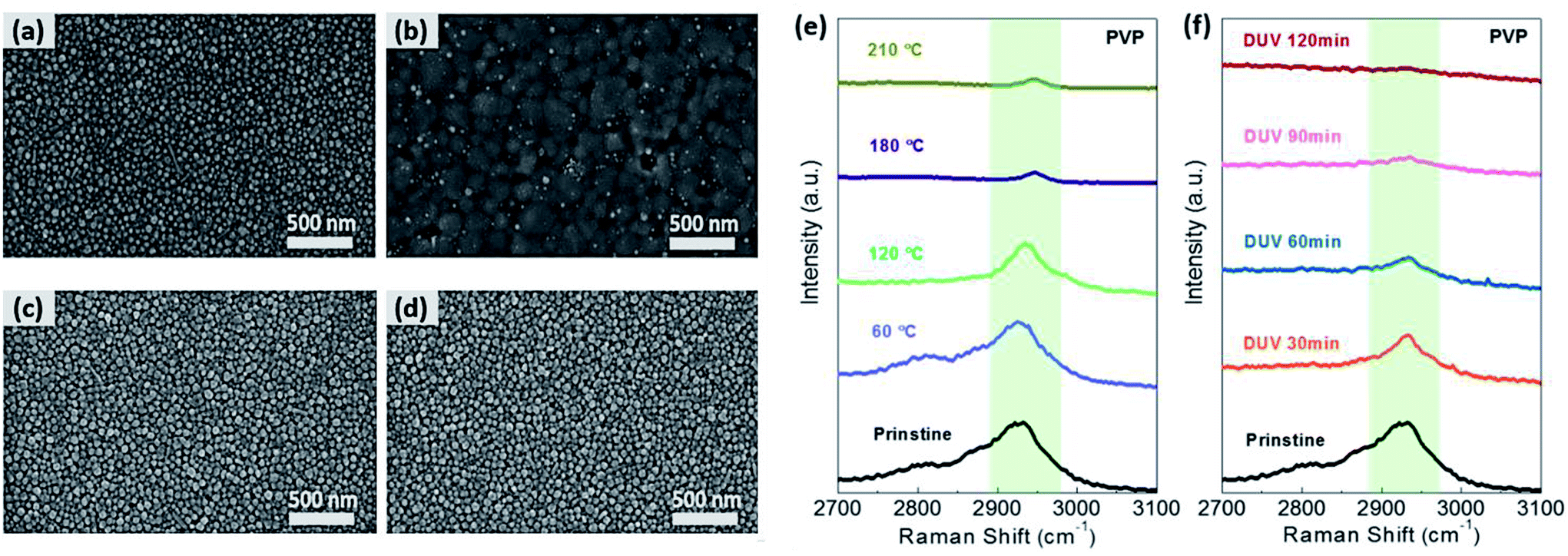 | ||
| Fig. 4 Morphology (FE-SEM) and chemical analysis (Raman) of the PVP-AgNPs with DUV and thermal treatment. (a and b) FESEM image of (a) pristine PVP-AgNPs and (b) thermally annealed PVP-AgNPs at 180 °C. (c and d) FESEM image of DUV treated PVP-AgNPs for (c) 60 min and (d) 90 min. (e and f) Variation of Raman spectrum of PVP-AgNP films obtained via (e) thermal and (f) DUV treatment. | ||
To demonstrate the removal of organic ligands more clearly, X-ray photoelectron spectra (XPS) of pristine and photochemical treated nanomaterial films were obtained. The C 1s or N 1s peaks were normalized with respect to Ag 3d or Bi 4f intensities, respectively. As shown in Fig. 5, S6 and S7 (ESI†), the pristine samples without photochemical treatment exhibit large amounts of carbon or nitrogen contents from organic surfactant. In contrast, the carbon or nitrogen contents are significantly reduced after photochemical treatment, which clearly indicates that the organic ligands are removed by DUV irradiation at relatively low temperature (room temperature).
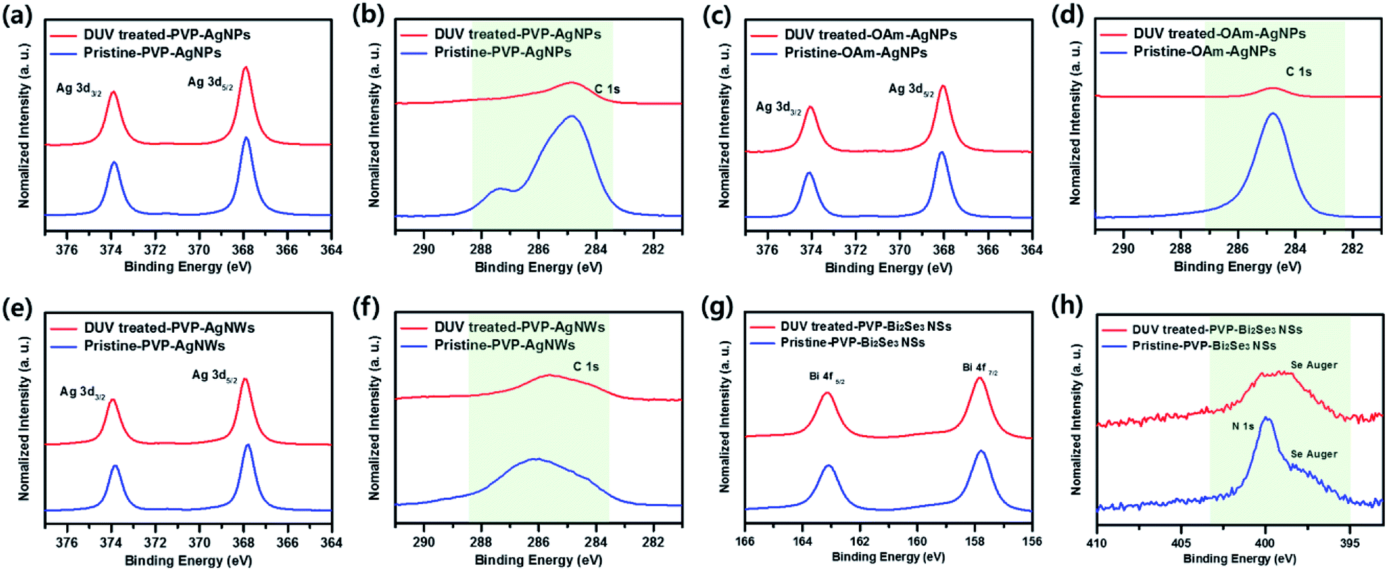 | ||
| Fig. 5 X-ray photoelectron spectroscopy analysis of C 1s (normalized to Ag 3d) and N 1s (normalized to Bi 4f) peaks for the before and after DUV treatment. ((a and d) PVP-AgNPs, (b and e) OAm-AgNPs, (c and f) PVP-AgNWs. (g and h) PVP-Bi2Se3 NSs). | ||
Conclusions
In this study, we confirmed that DUV treatment is an efficient method for the removal of the high-energy barrier polymeric or aliphatic organic ligands on the nanomaterials regardless of their morphology, such as NPs, NWs, and NSs. Although the NSs required additional excimer treatment to achieve the electronic properties, all of the DUV-treated materials exhibited much higher conductivities than the conductivities of thermally annealed samples. The thermally annealed AgNPs (PVP and OAm) showed the significant aggregation of sintered particles by the removal of ligands and thermal shrinkage, which cause void generation within AgNP films (>180 °C), whereas the DUV-treated AgNPs were sintered by nano-welding without significant film shrinkage. In particular, the DUV treated of PVP-AgNPs for 90 min (50–60 °C) resulted in a sheet resistance of 0.54 Ω □−1, while thermally treated PVP-AgNP had a sheet resistance of 7.5 kΩ □−1 at a similar annealing temperature of 60 °C. The Raman spectrum showed the additional evidence for the efficient removal of organic ligands, which indicates that the DUV-treatment is more effective than heat treatment, even at low temperature. In addition, the removal of organic ligands was confirmed more clearly from the reduction of the carbon content, as shown in XPS spectra. In conclusion, the photochemical treatment of nanomaterials is an efficient processing strategy for low-temperature-processed nanomaterial matrixes for next-generation flexible and wearable electronic devices.Conflicts of interest
There are no conflicts to declare.Acknowledgements
This research was partially supported by the Chung-Ang University Research Grants in 2017, and by the National Research Foundation of Korea (NRF) grant funded by the Korean government (No. 2017R1C1B2005254).References
- B. Cho, J. Yoon, M. G. Hahm, D.-H. Kim, A. R. Kim, Y. H. Kahng, S.-W. Park, Y.-J. Lee, S.-G. Park, J.-D. Kwon, C. S. Kim, M. Song, Y. Jeong, K.-S. Nam and H. C. Ko, J. Mater. Chem. C, 2014, 2, 5280–5285 RSC.
- X. Hu, X. Zhang, L. Liang, J. Bao, S. Li, W. Yang and Y. Xie, Adv. Funct. Mater., 2014, 24, 7373–7380 CrossRef CAS.
- Q. Hua, J. Sun, H. Liu, R. Bao, R. Yu, J. Zhai, C. Pan and Z. L. Wang, Nat. Commun., 2018, 9, 244 CrossRef PubMed.
- J. Jang, B. G. Hyun, S. Ji, E. Cho, B. W. An, W. H. Cheong and J.-U. Park, NPG Asia Mater., 2017, 9, e432 CrossRef CAS.
- D. Kim, Y. Fu, S. Kim, W. Lee, K. H. Lee, H. K. Chung, H. J. Lee, H. Yang and H. Chae, ACS Nano, 2017, 11, 1982–1990 CrossRef CAS PubMed.
- S. Wang, J. Xu, W. Wang, G. N. Wang, R. Rastak, F. Molina-Lopez, J. W. Chung, S. Niu, V. R. Feig, J. Lopez, T. Lei, S. K. Kwon, Y. Kim, A. M. Foudeh, A. Ehrlich, A. Gasperini, Y. Yun, B. Murmann, J. B. Tok and Z. Bao, Nature, 2018, 555, 83–88 CrossRef CAS PubMed.
- M. G. Kim, M. G. Kanatzidis, A. Facchetti and T. J. Marks, Nat. Mater., 2011, 10, 382–388 CrossRef CAS PubMed.
- C. Zhong, C. Duan, F. Huang, H. Wu and Y. Cao, Chem. Mater., 2011, 23, 326–340 CrossRef CAS.
- M. R. Niazi, R. Li, E. Qiang Li, A. R. Kirmani, M. Abdelsamie, Q. Wang, W. Pan, M. M. Payne, J. E. Anthony, D. M. Smilgies, S. T. Thoroddsen, E. P. Giannelis and A. Amassian, Nat. Commun., 2015, 6, 8598 CrossRef CAS PubMed.
- T. Sakanoue and H. Sirringhaus, Nat. Mater., 2010, 9, 736–740 CrossRef CAS PubMed.
- M. K. Choi, J. Yang, K. Kang, D. C. Kim, C. Choi, C. Park, S. J. Kim, S. I. Chae, T. H. Kim, J. H. Kim, T. Hyeon and D. H. Kim, Nat. Commun., 2015, 6, 7149 CrossRef CAS PubMed.
- J. H. Heo, M. H. Lee, H. J. Han, B. R. Patil, J. S. Yu and S. H. Im, J. Mater. Chem. A, 2016, 4, 1572–1578 RSC.
- Y. L. Rao, A. Chortos, R. Pfattner, F. Lissel, Y. C. Chiu, V. Feig, J. Xu, T. Kurosawa, X. Gu, C. Wang, M. He, J. W. Chung and Z. Bao, J. Am. Chem. Soc., 2016, 138, 6020–6027 CrossRef CAS PubMed.
- J. You, L. Meng, T. B. Song, T. F. Guo, Y. M. Yang, W. H. Chang, Z. Hong, H. Chen, H. Zhou, Q. Chen, Y. Liu, N. De Marco and Y. Yang, Nat. Nanotechnol., 2016, 11, 75–81 CrossRef CAS PubMed.
- W. Nie, H. Tsai, R. Asadpour, J.-C. Blancon, A. J. Neukirch, G. Gupta, J. J. Crochet, M. Chhowalla, S. Tretiak, M. A. Alam, H.-L. Wang and A. D. Mohite, Science, 2015, 347, 522–525 CrossRef CAS PubMed.
- X. Wang, F. Sun, Y. Duan, Z. Yin, W. Luo, Y. Huang and J. Chen, J. Mater. Chem. C, 2015, 3, 11397–11405 RSC.
- W. Ke, G. Fang, Q. Liu, L. Xiong, P. Qin, H. Tao, J. Wang, H. Lei, B. Li, J. Wan, G. Yang and Y. Yan, J. Am. Chem. Soc., 2015, 137, 6730–6733 CrossRef CAS PubMed.
- Y. S. Rim, H. Chen, X. Kou, H. S. Duan, H. Zhou, M. Cai, H. J. Kim and Y. Yang, Adv. Mater., 2014, 26, 4273–4278 CrossRef CAS PubMed.
- M. Akin, R. Bongartz, J. G. Walter, D. O. Demirkol, F. Stahl, S. Timur and T. Scheper, J. Mater. Chem., 2012, 22, 11529 RSC.
- R. M. Arán-Ais, F. J. Vidal-Iglesias, J. Solla-Gullón, E. Herrero and J. M. Feliu, Electroanalysis, 2015, 27, 945–956 CrossRef.
- S. Yu, C. Hwang, D. J. Kim, J. Park, S. Kim, J. Hong, J. An, T. H. Lee and M.-G. Kim, Thin Solid Films, 2018, 661, 46–52 CrossRef CAS.
- A. Nag, M. V. Kovalenko, J. S. Lee, W. Liu, B. Spokoyny and D. V. Talapin, J. Am. Chem. Soc., 2011, 133, 10612–10620 CrossRef CAS PubMed.
- D. Li, C. Wang, D. Tripkovic, S. Sun, N. M. Markovic and V. R. Stamenkovic, ACS Catal., 2012, 2, 1358–1362 CrossRef CAS.
- Z. Liu, M. Shamsuzzoha, E. T. Ada, W. M. Reichert and D. E. Nikles, J. Power Sources, 2007, 164, 472–480 CrossRef CAS.
- C.-H. Hwang, J.-P. Park, M.-Y. Song, J.-H. Lee and I.-W. Shim, Bull. Korean Chem. Soc., 2011, 32, 2207–2211 CrossRef CAS.
- B. Ingham, T. H. Lim, C. J. Dotzler, A. Henning, M. F. Toney and R. D. Tilley, Chem. Mater., 2011, 23, 3312–3317 CrossRef CAS.
- J. You, H. Ziruo, Y. Yang, Q. Chen, M. Cai, T.-B. Song, C.-C. Chen, S. Lu, L. Yongsheng, H. Zhou and Y. Yang, ACS Nano, 2014, 8, 1674–1680 CrossRef CAS PubMed.
- Z. Y. Chen, D. Liang, G. Ma, G. S. Frankel, H. C. Allen and R. G. Kelly, Corros. Eng., Sci. Technol., 2013, 45, 169–180 CrossRef.
- N. C. Anderson, M. P. Hendricks, J. J. Choi and J. S. Owen, J. Am. Chem. Soc., 2013, 135, 18536–18548 CrossRef CAS PubMed.
- P. R. Brown, D. Kim, R. R. Lunt, N. Zhao, M. G. Bawendi, J. C. B. Grossman and V. Bulovic, ACS Nano, 2014, 8, 5863–5872 CrossRef CAS PubMed.
- D. H. Webber and R. L. Brutchey, J. Am. Chem. Soc., 2012, 134, 1085–1092 CrossRef CAS PubMed.
- C. Hwang, J. An, B. D. Choi, K. Kim, S.-W. Jung, K.-J. Baeg, M.-G. Kim, K. M. Ok and J. Hong, J. Mater. Chem. C, 2016, 4, 1441–1447 RSC.
- G. Jiang, X. Li, M. Lan, T. Shen, X. Lv, F. Dong and S. Zhang, Appl. Catal., B, 2017, 205, 532–540 CrossRef CAS.
- J. Kim, M. G. Kim, J. Kim, S. Jo, J. Kang, J. W. Jo, W. Lee, C. Hwang, J. Moon, L. Yang, Y. H. Kim, Y. Y. Noh, J. Y. Jaung, Y. H. Kim and S. K. Park, Sci. Rep., 2015, 5, 14520 CrossRef CAS PubMed.
- Y. H. Kim, J. S. Heo, T. H. Kim, S. Park, M. H. Yoon, J. Kim, M. S. Oh, G. R. Yi, Y. Y. Noh and S. K. Park, Nature, 2012, 489, 128–132 CrossRef CAS PubMed.
- D. Tsvetanova, R. Vos, G. Vereecke, T. N. Parac-Vogt, F. Clemente, K. Vanstreels, D. Radisic, T. Conard, A. Franquet, M. Jivanescu, D. A. P. Nguyen, A. Stesmans, B. Brijs, P. Mertens and M. M. Heyns, J. Electrochem. Soc., 2011, 158, H785 CrossRef CAS.
- Y. Sun, B. Mayers, T. Herricks and Y. Xia, Nano Lett., 2003, 3, 955–960 CrossRef CAS.
- J. Perelaer, A. W. M. de Laat, C. E. Hendriks and U. L. Schubert, J. Mater. Chem., 2008, 18, 3209–3215 RSC.
- M. Chen, Y.-G. Feng, X. Wang, T.-C. Li, J.-Y. Zhang and D.-J. Qian, Langmuir, 2007, 23, 5296–5304 CrossRef CAS PubMed.
- Z. Lin, Y. Chen, A. Yin, Q. He, X. Huang, Y. Xu, Y. Liu, X. Zhong, Y. Huang and X. Duan, Nano Lett., 2014, 14, 6547–6553 CrossRef CAS PubMed.
- D. E. Xu, J. B. Kim, M. D. Hook, J. P. Jung and M. Mayer, J. Alloys Compd., 2018, 731, 504–514 CrossRef CAS.
- L. Mo, D. Liu, W. Li, L. Li, L. Wang and X. Zhou, Appl. Surf. Sci., 2011, 257, 5746–5753 CrossRef CAS.
- H. J. Hwang, K. H. Oh and H. S. Kim, Sci. Rep., 2016, 6, 19696 CrossRef CAS PubMed.
- K. Mallikarjuna, H.-J. Hwang, W.-H. Chung and H.-S. Kim, RSC Adv., 2016, 6, 4770–4779 RSC.
- M. M. Al-Shalalfeh, A. T. Onawole, T. A. Saleh and A. A. Al-Saadi, Mater. Sci. Eng., C, 2017, 76, 356–364 CrossRef CAS PubMed.
- R. G. Snyder, S. L. Hsu and S. Krimm, Spectrochim. Acta, 1978, 34A, 395–406 CrossRef CAS.
Footnotes |
| † Electronic supplementary information (ESI) available: [DETAILS]. See DOI: 10.1039/c8ra08173e |
| ‡ These two authors contributed equally to this work and are co-first authors. |
| This journal is © The Royal Society of Chemistry 2019 |