DOI:
10.1039/C8RA08107G
(Paper)
RSC Adv., 2019,
9, 3550-3557
CrO2-based heterostructure and magnetic tunnel junction: perfect spin filtering effect, spin diode effect and high tunnel magnetoresistance
Received
30th September 2018
, Accepted 17th January 2019
First published on 25th January 2019
Abstract
Half-metallic ferromagnetic CrO2 has attracted much interest due to its 100% spin polarization and high Curie temperature. CrO2 films have been fabricated on a TiO2 (100) substrate. However, there have been no reports on the spin transport properties of devices based on a CrO2 electrode and TiO2 barrier. In this work, we use first-principles calculations combined with a nonequilibrium Green's function method to investigate the bias-voltage-dependent spin transport properties for the CrO2/TiO2 (100) heterostructure and the CrO2/TiO2/CrO2 (100) magnetic tunnel junction (MTJ). Our results reveal the excellent spin filtering effect and spin diode effect in the heterostructure as well as the high tunnel magnetoresistance ratio (up to 4.48 × 10¹⁴%) in the MTJ, which indicate potential spintronic applications. The origins of these perfect spin transport characteristics are discussed in terms of the calculated spin-dependent electrode band structures, the spin-dependent transmission spectra and semiconductor theory.
1. Introduction
Spintronic devices, which use electronic spin or both electronic charge and spin to increase the data processing speed and decrease electric power consumption compared to conventional semiconductor devices, have attracted more and more research interest.1 One of the keys to high-performance spintronic devices is high spin injection efficiency from a magnetic material to a semiconductor, and thus high-spin-polarized materials are desired.2 Half-metallic magnets,3 which possess 100% spin polarization of electrons due to the fact that one of the two spin channels is metallic and the other has semiconductor or insulator characteristics, have been seen as promising candidates for high-spin-polarized materials and received extensive experimental and theoretical attention.4–8
Rutile CrO2 is one of the most famous spintronic materials due to its nearly 100% spin polarization and high Curie temperature (394 K).9–12 Rutile TiO2 is a semiconductor with the same crystal structure and comparable lattice constant with CrO2.13 So, TiO2 was usually used as the substrate to grow the CrO2 films. Bulk half-metallic ferromagnetic CrO2 is a metastable oxide phase that degrades at a high temperature (above 400 K) and atmospheric pressure into the thermodynamically more stable antiferromagnetic insulator Cr2O3 phase,14 and there are more or less Cr2O3 at the surface of CrO2,15–17 however, with the improvement of experimental technology and the control of growth condition, single crystal CrO2 films with a better crystalline quality and different orientations have been successfully grown on the TiO2 (100), TiO2 (001) and TiO2 (110) substrates by the chemical vapor deposition technique.17–20
For the spintronic applications, there have been some studies on electronic transport properties based on CrO2 electrode.21–26 Meena and Choudhary21–25 systemically investigated the spin transport properties for some magnetic tunnel junctions (MTJs) based on CrO2 electrode and different barriers such as the graphene and the carbon nanotube, and large tunneling magnetoresistance (TMR) ratios were predicted. Leo et al.26 experimentally studied the TMR in the MTJ of CrO2/MgO/CoFe (100), and revealed that the TMR sign can be reversed simply by subtle modifications to the CrO2/MgO interface. In addition, some MTJs, where TiO2 as the barrier and other magnetic materials instead of CrO2 as the electrodes, have also been explored.27–30 These studies indicated that the large TMR ratio is related to the electrode with high spin polarization and the property of tunnel barrier in the MTJ. As far as we know, however, there is no report on the spin transport properties of the MTJ of CrO2/TiO2/CrO2, considering the facile growth of the CrO2 films on the TiO2 (100) substrate,17,20 it is meaningful to explore the potential spintronic applications for the CrO2/TiO2 (100) heterostructure and the CrO2/TiO2/CrO2 (100) MTJ. In the present work, our calculations based on the first-principles combined with the nonequilibrium Green's function method reveal that the CrO2/TiO2 (100) heterostructure behaves obvious spin diode effect and spin filtering effect, and the CrO2/TiO2/CrO2 (100) MTJ has a high TMR ratio (up to 4.48 × 10¹⁴%). These results could be helpful for the experimental realization of CrO2-based spintronic devices.
2. Computational details
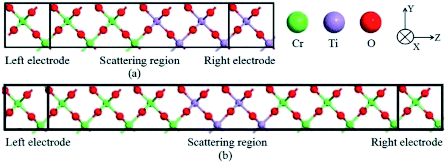
Rutile CrO2 belongs to the tetragonal structure (P42/mnm) with lattice parameters a = b = 4.421 Å and c = 2.916 Å,31 while isostructural TiO2 has the lattice parameters a = b = 4.594 Å and c = 2.958 Å.32 Considering the experimental growth of CrO2 (100) films on the TiO2 (100) substrates and the small lattice mismatch along (100) direction (1.72%), we construct the CrO2/TiO2 (100) heterostructure and the CrO2/TiO2/CrO2 (100) MTJ based on the TiO2 lattice constant. As shown in Fig. 1, both models of the two devices are divided into three parts: the left electrode, the scattering region, and the right electrode. Note that there are four possible contacts for the interface between CrO2 and TiO2:Cr–O interface (type-I), Cr–Ti interface (type-II), O–Ti interface (type-III) and O–O interface (type-IV). We relax the four interfaces and the calculated total energies are −8752.1461, −8750.3011, −8751.7887 and −8749.9607 eV per cell for the four interfaces, respectively, which indicate that the type-I configuration is most stable relatively. So, in our present work, we focus on the type-I structure for the transport properties of the heterostructure and the MTJ.
 |
| | Fig. 1 Schematic illustrations of the devices of the CrO2/TiO2 (100) heterostructure (a) and the CrO2/TiO2/CrO2 (100) magnetic tunnel junction (MTJ) (b). The z direction is the transmission direction. | |
Our calculations are performed by the Atomistix ToolKit (ATK) package, which combines the nonequilibrium Green's function (NEGF) and the density functional theory (DFT).33,34 The generalized gradient approximation (GGA) with the Perdew–Burke–Ernzerhof (PBE) form is adopted for the electronic exchange–correlation functional.35 Before calculating the transport properties, the interface relaxation is carried out until the force on each atom is less 0.01 eV Å−1. The electron wave function of the linear combination of atomic orbitals (LCAO) is cut off at a kinetic energy of 2041 eV, and the Brillouin zone of the unit cell is sampled by using a 6 × 4 × 1 k-point grid. In the calculations of transport properties, the Monkhorst–Pack k-meshes of both devices are 6 × 4 × 100, the integration grid of the current calculation is 10 × 10, and the self-consistent calculations are limited to 2.7 × 10⁻⁴ eV tolerance. All these parameters are tested to be sufficient to obtain accurate results, and the present method has been successfully used in our previous works on spin transport properties of magnetic heterostructures and MTJs.36,37 The spin-dependent current is calculated by the Landauer-Buttiker formula:
| |
 | (1) |
where
fL/R(
E −
μL/R) is the Fermi–Dirac distribution for the left (right) electrode, and
μL/R =
EF ±
eV/2 is the corresponding electrochemical potential.
T↑(↓)(
E,
Vb) is the spin-dependent transmission coefficient,
| | |
T↑(↓)(E,Vb) = Tr[ΓLGRΓRGA]↑(↓),
| (2) |
where
GR(A) is the retarded (advanced) Green's function of the central region, and
ΓL(R) is the coupling matrix of the left (right) electrode.
3. Results and discussion
3.1. Spin diode and spin filtering effects in the CrO2/TiO2 heterostructure
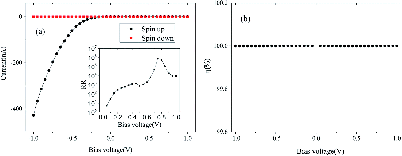
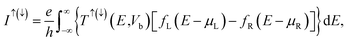
We first study the spin transport properties of the CrO2/TiO2 (100) heterostructure. The spin-resolved current is calculated under the bias voltage range from −1 V to 1 V, as shown in Fig. 2. It is clear that the spin-down current is absolutely inhibited. For the spin-up current, the value is close to zero when the applied voltage is positive. When the negative voltage is applied, however, the spin-up current rapidly increases with the increasing negative bias voltage. Hence the heterostructure exhibits perfect spin diode effect in the spin-up channel and successfully filters out the spin-down current. The rectification ratio,38 RR(V) = |I(−V)/I(V)|, is usually used to evaluate the diode performance, and a large rectification ratio means a good diode effect. Fig. 2 indicates that the largest RR value in the spin-up channel reaches 7.8 × 10⁵ at 0.75 V. Such a large RR indicates excellent unidirectional conductivity, making CrO2 a promising candidate for spin diode application. In addition, we calculate the efficient of the spin filtering by η = [(I↑ − I↓)/(I↑ + I↓)] × 100%, where I↑ and I↓ are the spin-up and spin-down currents, respectively.39 As shown in Fig. 2(b), the efficiency of the spin filtering is almost complete.
 |
| | Fig. 2 (a) The spin-dependent current-bias voltage curve of the CrO2/TiO2 (100) heterostructure. The inset is the rectification ratio (RR) in spin-up channel with the change of bias voltage. (b) The spin-filtering efficiency η (in %) versus bias voltage. | |
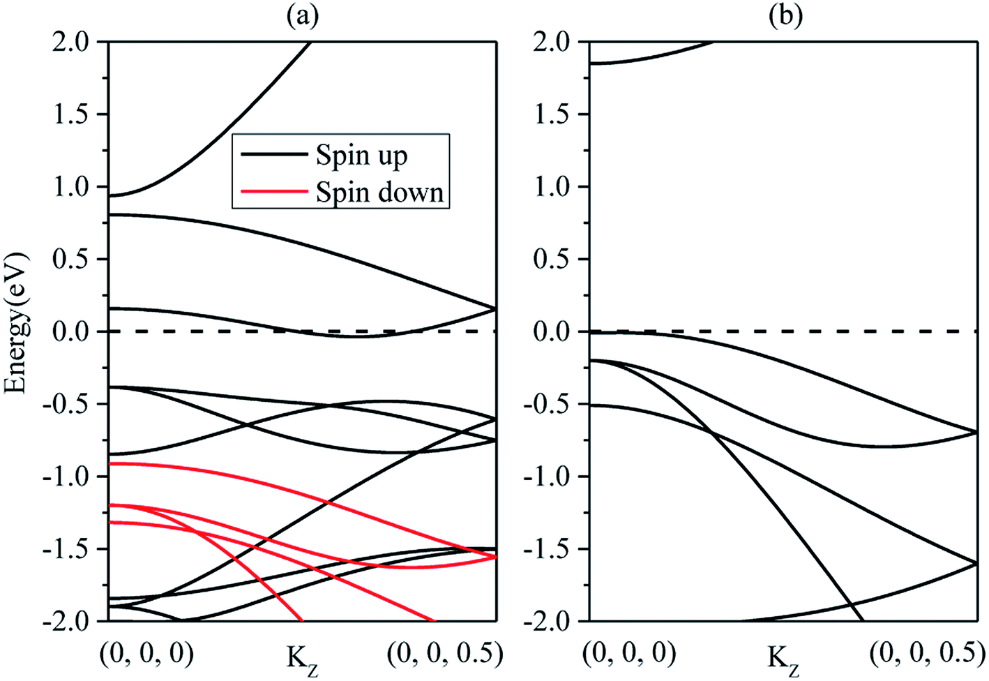
We further present in Fig. 3 the calculated spin-dependent band structures of the left electrode CrO2 (100) and the right electrode TiO2 (100) in order to explain the spin-dependent current–voltage curve. One can see from Fig. 3 that the left electrode CrO2 is a typical half-metal: a metallic characteristic in the spin-up channel and the Fermi-level falls in a large energy gap in the spin-down channel. The top of the spin-down valence bands is about 0.91 eV below the Fermi level at the (000) k point, and the bottom of the spin-down conduction bands is about 3.64 eV above the Fermi level at the same k point. For the right electrode TiO2 (100), the top of the valence bands is tangent to the Fermi level and there is a wide band gap above the Fermi level. According to the electrochemical potentials of the left and right electrodes, μL/R = EF ± (1/2)eVb, the Fermi level of the left electrode (right electrode) will move down (up) (1/2)eVb when a positive bias voltage Vb is applied. Therefore, in the applied voltage range from 0 V to 1 V, the spin-up valence bands of the left electrode cross the Fermi level and the transmission channel is generated in the spin-up channel of the left electrode. At the same time, the Fermi level of the right electrode falls in the semiconductor gap. Such a big gap could not motivate the right electrode to produce transmission channel. Hence, either in the spin-up or spin-down state, the Bloch states of the left electrode are unable to go through the right electrode at a positive bias voltage, because there is no transmission channel to receive them. So, the forward current in both spin channels is zero at the positive bias voltage range. However, when the negative bias voltage is applied to the device, the spin-up conduction bands of the left electrode cross the Fermi level, and thus some transmission channels are generated. Meanwhile, the Fermi level of the right electrode moves down, and in turn, the valence bands of right electrode cross the Fermi level, producing transmission channels. The well match of the spin-up resonance channels of two electrodes provides the transmission condition. This is similar to the open-circuit state. With the increase of the negative bias voltage, more and more bands cross the Fermi level, resulting in the increase of the transmission channels and the spin-up current, and thus the diode effect emergences in the spin-up channel. In the bias voltage range, the spin-down bands of CrO2 are never able to cross the Fermi level due to the relatively wide band gaps above and below the Fermi level in the spin-down channel of the CrO2 electrode. Therefore, there is no Bloch state in the spin-down channel and the spin-down current is zero, resulting in the spin filtering effect at the negative bias voltage.
 |
| | Fig. 3 Band structures along the (100) direction for the left electrode CrO2 (a) and the right electrode TiO2 (b). The dashed line means the Fermi level at zero eV. | |
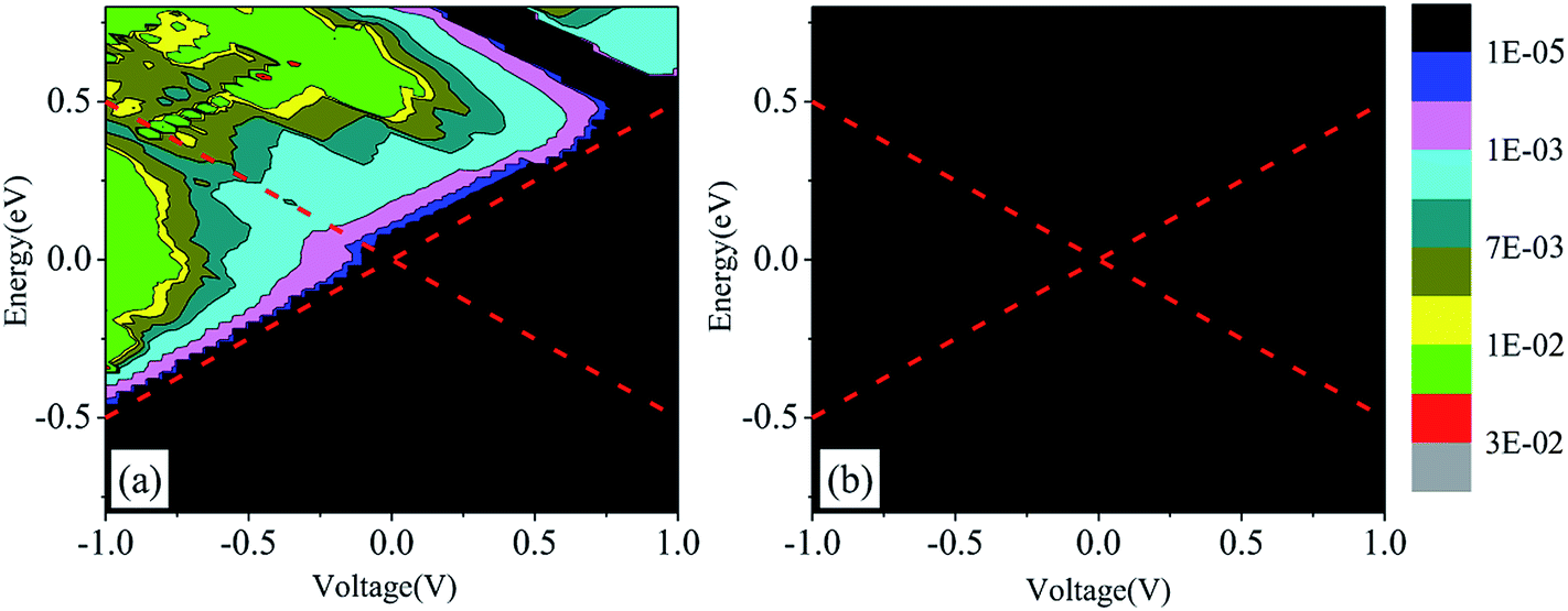
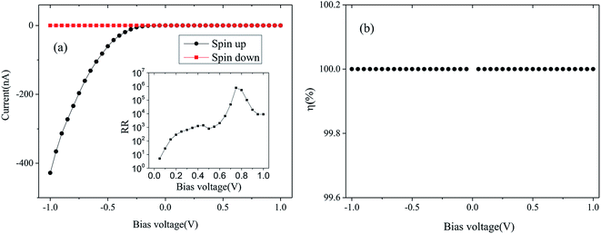
To further understand the mechanism of the spin diode effect and the spin filtering effect, we show in Fig. 4 the calculated bias voltage-dependent transmission spectra. The red dotted lines represent the electrochemical potentials of the left/right electrode, and the area between lines denotes the bias window. Note that the spin-polarized current can be obtained through the energy integral of transmission coefficients over the bias window. For the spin-up transmission spectra (Fig. 4(a)), there is no transmission coefficient in the positive bias window. So, the spin-up current is zero at the positive bias voltage. However, different phenomenon appears in the negative bias window, i.e., with the increase of the negative bias voltage, the transmission coefficient value becomes more and more large, and the area of bias window becomes broader and broader. So, the spin-up current increases with increasing negative bias voltage, i.e., the diode effect appears in the spin-up channel. However, for the spin-down transmission spectra (Fig. 4(b)), neither negative nor positive bias window is filled with transmission coefficient. So, the spin-down current is inhibited, leading to the spin filtering effect in the negative bias voltage range.
 |
| | Fig. 4 The spin-dependent transmission spectra in the spin-up (a) and spin-down (b) channels for the CrO2/TiO2 (100) heterostructure. | |
3.2. High tunnel magnetoresistance in the CrO2/TiO2/CrO2 magnetic tunnel junction
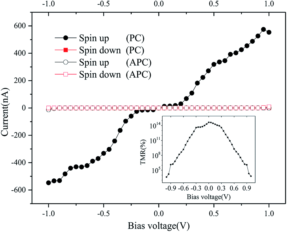
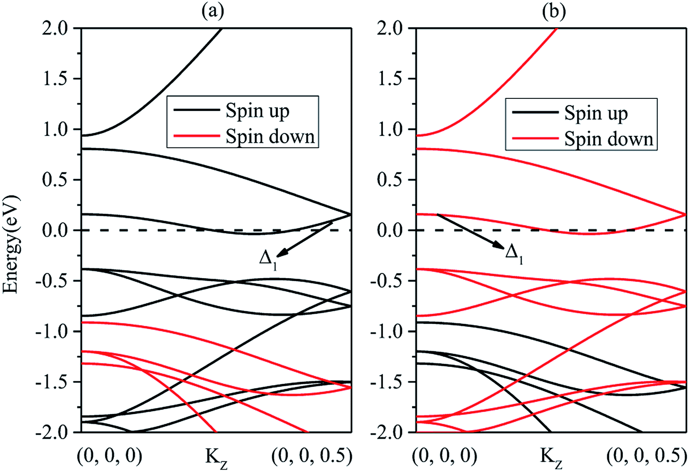
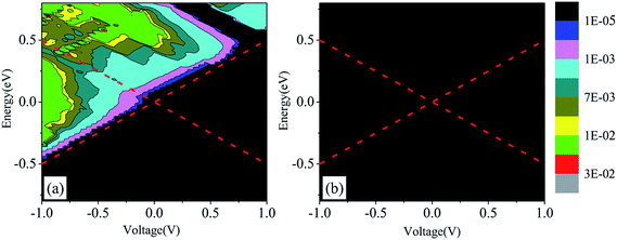
We now calculate the spin transport properties of the CrO2/TiO2/CrO2 (100) MTJ. The parallel magnetization configuration (PC) and the antiparallel magnetization configuration (APC) between the left and right CrO2 electrodes are considered. Fig. 5 shows the calculated spin-dependent current with the change of bias voltage in the PC and APC. One can see clearly from Fig. 5 that the spin-down current in the PC and both spin-up and spin-down currents in the APC are almost zero in the bias voltage range considered. Only the spin-up current in the PC is considerable and it rapidly increases with increasing bias voltage. These distinctive I–V characteristics lead to the large TMR ratio, as shown in the inset of Fig. 5, it reaches 4.48 × 10¹⁴% at zero bias voltage. Note that, there are usually three definitions of the TMR value: the “optimistic”, the “pessimistic” and the “normalized” TMR.40 Here, we adopt the optimistic TMR = [(IP − IAP)/IAP] × 100%, where IP (IAP) is the total (spin-up plus spin-down) current for the MTJ in the PC (APC).40 To explain the I–V characteristics and the large TMR ratio, we calculate the spin-dependent band structures of the CrO2 electrode in the PC and APC (Fig. 6). For the PC, the magnetization directions of two electrodes are same, and thus the band structure of the left electrode (Fig. 6(a)) is identical to that of the right electrode (Fig. 6(a)). When a positive bias voltage is applied to the MTJ, the Fermi level of the left electrode moves down, and the Fermi level of the right electrode moves up. Due to the metallic properties in the spin-up direction, the Fermi levels of two electrodes always cross the bands and the transmission channels are generated in the spin-up channel of two electrodes simultaneously. So, the Bloch states started in the left electrode can be well received in the right electrode. With the increase of applied bias voltage, the spin-up current is increased. The same situation also appears in the case of the negative bias voltage. At the same time, we also note the semiconductor characteristic with a large energy gap in the spin-down channel. No matter what the bias voltage is applied in the PC, the large band gap always prevents the generation of transmission channels in the spin-down channel, and thus there is no spin-down current in the PC.
 |
| | Fig. 5 The spin-dependent current-bias voltage curve of the CrO2/TiO2/CrO2 (100) MTJ in the PC and the APC. The inset shows the TMR with the change of bias voltage. | |
 |
| | Fig. 6 Band structures along the (100) direction for the left and right electrodes of the CrO2/TiO2/CrO2 (100) MTJ in the PC [(a) and (a)] and the APC [(a) and (b)]. | |
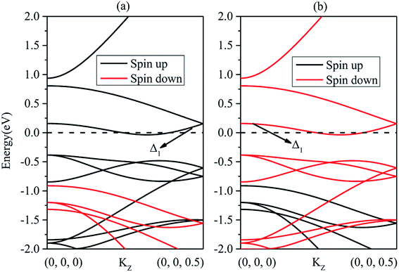
For the APC, the magnetization directions of two electrodes are completely opposite. That is, the spin-up bands and the spin-down bands are exchanged between the two electrodes. So, the band structures of the left and right electrodes correspond to Fig. 6(a) and (b), respectively. This spin-dependent inverse band structures between two electrodes and the large energy gap in one of the two spin channels result in the mismatch of the transmission channels no matter a positive or a negative bias voltage is applied, and in turn, both the spin-up and spin-down currents in the APC are suppressed. Therefore, the negligible current in the APC make the TMR ratio large. In order to explain the largest TMR value at the zero bias voltage (Fig. 5), we list in Table 1 the typical transport properties of the CrO2/TiO2/CrO2 (100) MTJ. For the spin-up channel in the PC, the maximum transmission coefficient reaches 0.184, which is relatively larger in transport. It is to say, the incoming wave function of the left electrode Δ1 band (Fig. 6) is slightly scattered and the right electrode receives most of the incoming wave. For the spin-down channel in the PC, the transmission coefficient is much smaller than that in the spin-up channel, because the incoming wave function of Δ1 band is nearly nonexistent. According to the definition of spin polarization, SP = [(G↑ − G↓)/(G↑ + G↓)] × 100%, where G↑ and G↓ are the spin-up and spin-down conductions, respectively. The calculated spin polarization in the PC reaches 100%. This indicates that the CrO2 electrode is a good spin injection source for the device. For the spin-up and spin-down channels in the APC, the maximum transmission coefficients are very small, because the incoming wave function of Δ1 band only appears in one spin channel, and there is no corresponding Δ1 symmetry state to receive them. Therefore, the incoming wave always decays along the transport direction, and both spin-up and spin-down conductions in the APC are very small. The great differences of TMAX and G between the PC and APC at zero bias voltage result in the huge TMR ratio.
Table 1 Calculated spin transport properties of the CrO2/TiO2/CrO2 (100) MTJ in the parallel magnetization configuration (PC) and the antiparallel magnetization configuration (APC). TMAX is the largest transmission coefficient, G is the quantum conduction, and SP is the spin polarization at zero bias voltage for the MTJ
| |
TMAX |
G (siemens) |
SP (%) |
| Spin-up in PC |
1.84 × 10⁻¹ |
3.68 × 10⁻⁷ |
100.00% |
| Spin-down in PC |
2.03 × 10⁻¹⁶ |
1.95 × 10⁻²² |
|
| Spin-up in APC |
4.04 × 10⁻¹⁴ |
8.22 × 10⁻²⁰ |
99.99% |
| Spin-down in APC |
3.67 × 10⁻¹⁸ |
4.72 × 10⁻²⁴ |
|
It should be pointed out that the TMR value is usually dependent on the thickness of the barrier, so we further calculate the TiO2 layers dependence of TMR ratio, as shown in Fig. 7. It shows that the TMR value oscillates with the increase of the barrier thickness, but it still reaches ∼1014% when the thickness of the barrier is increased to three or four TiO2 units. According to the Julliere model, TMR ratio is determined by spin polarization of both electrodes and irrelevant to barrier thickness.41 The TMR oscillatory indicates that the coherency of electron wave functions is conserved across the barrier, and TiO2 plays a selective filtration role in transport mechanism.
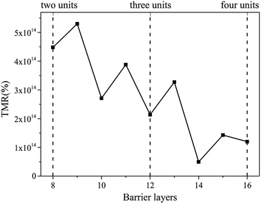 |
| | Fig. 7 The TiO2 barrier thickness dependence of the TMR ratio in the CrO2/TiO2/CrO2 (100) MTJ. The three dashed lines represent the thickness of two, three and four TiO2 units, respectively. | |
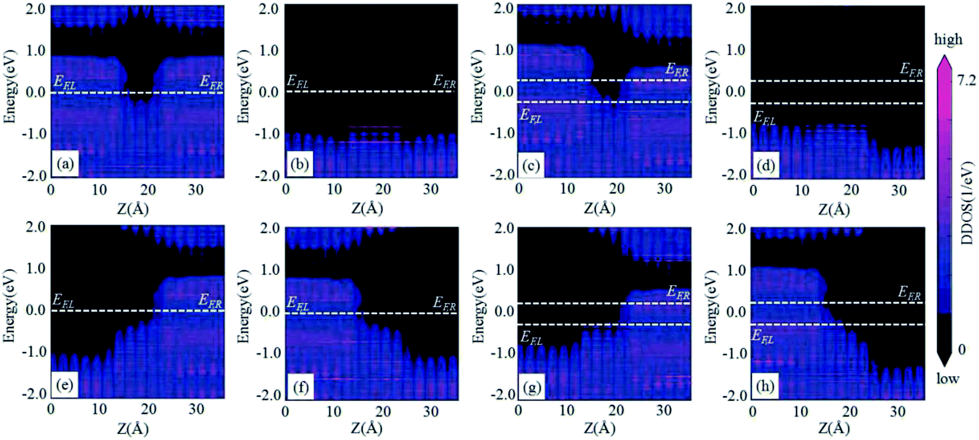
Finally, we use the semiconductor theory to explain the current change with bias voltage in different magnetization configurations of the CrO2/TiO2/CrO2 (100) MTJ. Fig. 8 indicates the calculated spin-dependent device density of states (DDOS). When the applied voltage is zero in the PC, the Fermi levels of left and right electrodes are located at the same energy level, as shown in Fig. 8(a) and (b). It is found that the device is a typical metal–semiconductor–metal (MSM)42 structure in the spin-up channel, and the apparent metal induced gap states (MIGS) are formed at the region of TiO2 due to the Fermi level pinning of semiconductor and metal.43 During the pinging process, the Schottky barriers appear on the two metal–semiconductor interfaces. Under a positive bias voltage such as 0.5 V [Fig. 8(c)], the Fermi level of the left electrode shifts down, leading to the decrease of the barrier height around the left interface of the device. A lot of holes coming from the left electrode begin to inject into the TiO2 intrinsic semiconductor. The rising Fermi level of the right electrode makes electrons inject into TiO2 barrier from right to left. TiO2 stores a lot of electrons and holes, and these carriers recombination causes TiO2 resistivity to be lower. So, the higher the bias voltage between two electrodes, the bigger the passing spin-up current in the MSM structure. For the spin-down channel of the PC (Fig. 8(b) and (d)), the device is made of three wide band gap semiconductors. There is no carrier within bias window under a positive bias voltage. So, the high insulation resistance device generates negligible current. Fig. 8(e)–(h) are the spin-dependent DDOS in the APC under the bias voltages of zero and 0.5 V. In both spin-up and spin-down states, the devices are composed of the insulator–semiconductor–metal structure or the metal–semiconductor–insulator structure, which are similar to the metal–insulator–semiconductor (MIS) structure.44 MIS plays the role of capacitor in the circuit and the electric conductive performance is poor, because there is no charge in the insulator region. So, the currents at positive bias voltage in the APC are very small and negligible, and this similar phenomenon is also found at the negative bias voltage in the APC (not shown here).
 |
| | Fig. 8 The spin-dependent device density of states (DDOS) for the CrO2/TiO2/CrO2 (100) MTJ at the bias voltages of zero V in the PC [(a) and (b)], 0.5 V in the PC [(c) and (d)], zero V in the APC [(e) and (f)] and 0.5 V in the APC [(g) and (h)]. [(a), (c), (e) and (g)] and [(b), (d), (f) and (h)] represent the spin-up and spin-down channels, respectively. | |
4. Conclusion
Half-metallic CrO2 with 100% spin polarization make it meaningful to study the spin transport properties of the spintronic devices based on the CrO2 electrode. Motivated by the experimental growth of the CrO2 (100) films on TiO2 (100) substrate, we construct the spintronic devices of the CrO2/TiO2 (100) heterostructure and the CrO2/TiO2/CrO2 (100) MTJ. By using the first-principles calculations combined with the nonequilibrium Green's function, we predict the excellent spin diode and spin filtering effects in the heterostructure as well as the high TMR ratio in the MTJ, which indicate the potential spintronic applications of CrO2. We also discuss the formation mechanism of these perfect spin transport properties from the calculated spin-dependent electrode band structures, the transmission spectra and the device density of states.
Conflicts of interest
There are no conflicts to declare.
Acknowledgements
This work was supported by the National Natural Science Foundation of China under Grant No. 11474113 and No. 11504278.
References
- A. Hirohata and K. Takanashi, J. Phys. D: Appl. Phys., 2014, 47, 193001 CrossRef.
- G. Schmidt, D. Ferrand, L. W. Molenkamp, A. T. Filip and B. J. van Wees, Phys. Rev. B: Condens. Matter Mater. Phys., 2000, 62, R4790–R4793 CrossRef CAS.
- R. A. de Groot, F. M. Mueller, P. G. V. Engen and K. H. J. Buschow, Phys. Rev. Lett., 1983, 50, 2024–2027 CrossRef CAS.
- H. C. Kandpal, G. H. Gerhard and C. Felser, J. Phys. D: Appl. Phys., 2007, 40, 1507–1523 CrossRef CAS.
- X. Wu, J. Han, Y. Feng, G. Li, C. Wang, G. Ding and G. Gao, RSC Adv., 2017, 7, 44499–44504 RSC.
- J. He, P. Lyu and P. Nachtigall, J. Mater. Chem. C, 2016, 4, 11143–11149 RSC.
- R. Hu, Z. H. Zhang and Z. Q. Fan, Phys. Chem. Chem. Phys., 2017, 19, 20137–20146 RSC.
- M. M. Monshi, S. M. Aghaei and I. Calizo, RSC Adv., 2016, 7, 18900–18908 RSC.
- K. Schwarz, J. Phys. F: Met. Phys., 1986, 16, L211 CrossRef CAS.
- Y. Ji, G. J. Strijkers, F. Y. Yang, C. L. Chien, J. M. Byers, A. Anguelouch, G. Xiao and A. Gupta, Phys. Rev. Lett., 2001, 86, 5585–5588 CrossRef CAS PubMed.
- A. Anguelouch, A. Gupta, G. Xiao, D. W. Abraham, Y. Ji, S. Ingvarsson and C. L. Chien, Phys. Rev. B: Condens. Matter Mater. Phys., 2001, 64, 180408(R) CrossRef.
- T. J. Swoboda, P. Arthur, N. L. Cox, J. N. Ingraham, A. L. Oppegard and M. S. Sadler, J. Appl. Phys., 1961, 32, 374S–375S CrossRef.
- D. O. Scanlon, C. W. Dunnill, J. Buckeridge, S. A. Shevlin, A. J. Logsdail, S. M. Woodley, C. R. Catlow, M. J. Powell, R. G. Palgrave, I. P. Parkin, G. W. Watson, T. W. Keal, P. Sherwood, A. Walsh and A. A. Sokol, Nat. Mater., 2013, 12, 798–801 CrossRef CAS PubMed.
- L. W. Fringer and R. M. Hazen, J. Appl. Phys., 1980, 51, 5362 CrossRef.
- R. Cheng, B. Xu, C. N. Borca, A. Sokolov, C. S. Yang, L. Yuan, S. H. Liou, B. Doudin and P. A. Dowben, Appl. Phys. Lett., 2001, 79, 3122 CrossRef CAS.
- J. Dho, D.-H. Kim, D. Kwon and B. G. Kim, J. Appl. Phys., 2008, 104, 063528 CrossRef.
- H. Fujiwara, M. Sunagawa, K. Terashima, T. Kittaka, T. Wakita, Y. Muraoka and T. Yokoya, Appl. Phys. Lett., 2015, 106, 202404 CrossRef.
- P. B. Visscher, P. R. LeClair and A. Gupta, Appl. Phys. Lett., 2013, 102, 162410 CrossRef.
- K. B. Chetry, M. Pathak, P. LeClair and A. Gupta, J. Appl. Phys., 2009, 105, 083925 CrossRef.
- M. Rabe, J. Pommer, K. Samm, B. Özyilmaz, C. König, M. Fraune, U. Rüdiger, G. Güntherodt, S. Senz and D. Hesse, J. Phys.: Condens. Matter, 2002, 14, 7 CrossRef CAS.
- S. Meena and S. Choudhary, Phys. Chem. Chem. Phys., 2017, 19, 17765–17772 RSC.
- S. Meena and S. Choudhary, Phys. Lett. A, 2017, 381, 3431–3439 CrossRef CAS.
- S. Meena and S. Choudhary, AIP Adv., 2017, 7, 125008 CrossRef.
- S. Meena and S. Choudhary, Mater. Chem. Phys., 2018, 217, 175–181 CrossRef CAS.
- A. K. Singh, S. Choudhary and S. Meena, J. Supercond. Novel Magn., 2018, 31, 2753–2758 CrossRef CAS.
- T. Leo, C. Kaiser, H. Yang, S. S. P. Parkin, M. Sperlich, G. Güntherodt and D. J. Smith, Appl. Phys. Lett., 2007, 91, 252506 CrossRef.
- V. Garcia, M. Bibes, A. Barthélémy, M. Bowen, E. Jacquet, J. P. Contour and A. Fert, Phys. Rev. B: Condens. Matter Mater. Phys., 2004, 69, 052403 CrossRef.
- K. M. Kim, B. J. Choi, M. H. Lee, G. H. Kim, S. J. Song, J. Y. Seok, J. H. Yoon, S. Han and C. S. Hwang, Nanotechnology, 2011, 22, 254010 CrossRef PubMed.
- M. Bibes, M. Bowen, A. Barthélémy, A. Anane, K. Bouzehouane, C. Carrétéro, E. Jacquet, J. P. Contour and O. Durand, Appl. Phys. Lett., 2003, 82, 3269–3271 CrossRef CAS.
- H. Mahmoudi, T. Windbacher, V. Sverdlov and S. Selberherr, 21st International Conference “MIXDES 2014”, Lublin, Poland, 2014, June 19–21, pp. 58–61 Search PubMed.
- M. S. Anwar and J. Aarts, Phys. Rev. B: Condens. Matter Mater. Phys., 2013, 88, 085123 CrossRef.
- J. K. Burdett, T. Hughbanks, G. J. Miller, J. W. Richardson Jr and J. V. Smith, J. Am. Chem. Soc., 1987, 109, 3639–3646 CrossRef CAS.
- J. Taylor, H. Guo and J. Wang, Phys. Rev. B: Condens. Matter Mater. Phys., 2001, 63, 245407 CrossRef.
- M. Brandbyge, J.-L. Mozos, P. Ordejón, J. Taylor and K. Stokbro, Phys. Rev. B: Condens. Matter Mater. Phys., 2002, 65, 165401 CrossRef.
- J. P. Perdew, K. Burke and M. Ernzerhof, Phys. Rev. Lett., 1996, 77, 3865 CrossRef CAS PubMed.
- G. Y. Gao and K. L. Yao, Appl. Phys. Lett., 2014, 105, 182405 CrossRef.
- J. Li, G. Gao, Y. Min and K. Yao, Phys. Chem. Chem. Phys., 2016, 18, 28018–28023 RSC.
- Z. Zhu, Z. H. Zhang, D. Wang, X. Q. Deng, Z. Q. Fan and G. P. Tang, J. Mater. Chem. C, 2015, 3, 9657–9663 RSC.
- J. Zeng and K. Q. Chen, J. Mater. Chem. C, 2015, 3, 5697–5702 RSC.
- X. Feng, O. Bengone, M. Alouani, I. Rungger and S. Sanvito, Phys. Rev. B: Condens. Matter Mater. Phys., 2009, 79, 214432 CrossRef.
- M. Julliere, Phys. Lett., 1975, 54A, 225–226 CrossRef CAS.
- S. M. Sze, D. J. Coleman and A. Loya, Solid-State Electron., 1971, 14, 1209–1218 CrossRef CAS.
- V. Heine, Phys. Rev., 1965, 138, A1689 CrossRef.
- P. Cova, A. Singh and R. A. Masut, J. Appl. Phys., 1997, 82, 5217 CrossRef CAS.
|
| This journal is © The Royal Society of Chemistry 2019 |
Click here to see how this site uses Cookies. View our privacy policy here. 
 Open Access Article
 This Open Access Article is licensed under a Creative Commons Attribution-Non Commercial 3.0 Unported Licence
 *ac
*ac