
 Open Access Article
 This Open Access Article is licensed under a Creative Commons Attribution-Non Commercial 3.0 Unported Licence
Graphene/Si Schottky solar cells: a review of recent advances and prospects
Xinyi
Kong
,
Linrui
Zhang
,
Beiyun
Liu
,
Hongli
Gao
,
Yongzhe
Zhang
 ,
Hui
Yan
and
Xuemei
Song
*
,
Hui
Yan
and
Xuemei
Song
*
College of Material Science and Engineering, College of Applied Sciences, Beijing University of Technology, Beijing 100124, China. E-mail: sxm@bjut.edu.cn; Tel: +86-010-67392533
First published on 8th January 2019
Abstract
Graphene has attracted tremendous interest due to its unique physical and chemical properties. The atomic thickness, high carrier mobility and transparency make graphene an ideal electrode material which can be applied to various optoelectronic devices such as solar cells, light-emitting diodes and photodetectors. In recent years, there has been a growing interest in developing graphene/silicon Schottky junction solar cells and the power conversion efficiency has reached up to 15.8% with an incredible speed. In this review, we introduce the structure and mechanism of graphene/silicon solar cells briefly, and then summarize several key strategies to improve the performance of the cells. Finally, the challenges and prospects of graphene/silicon solar cells are discussed in the development of the devices in detail.
1. Introduction
As the population continuously grows, the rising environmental pollution and increasing energy demand have created a surge in exploring renewable, clean energy sources other than fossil fuels. Among the various renewable energy sources such as tidal energy, wind energy and so on, solar cells have drawn tremendous interest and are being investigated intensively to meet the greatly increasing demand for clean energy.1 To date, solar cells have experienced generations with the core photovoltaic conversion material ranging from p–n junction solar cells, dye solar cells (DSCs), and perovskite solar cells. Dye solar cells (DSCs) have drawn tremendous interest due to their low-cost, environment friendly nature and low-energy manufacturing process,2 but the maximum efficiency is only 13.0%.3 Solid state perovskite solar cells, have reached efficiency as high as 22.1%,4 but there is a great challenge that it has a low stability, the cells currently only last for months outdoors, whereas silicon solar panels are usually guaranteed to work for at least 25 years. Although various light-harvesting materials have been explored and developed in solar cells, so far, silicon is the most representative because of its broad absorption band. The efficiency of a conventional silicon solar cells based on p–n junction could exceed 26.6% as reported in 2017.5 In addition to its high power conversion efficiency, the dominant role of p–n junction-based silicon solar cell in the market results from highly commercialized fabrication techniques. However, these involved techniques usually require high temperature ion diffusion and expensive ion implantation processes to introduce dopants into silicon substrate.6 Despite of the complicated processes, they are of high pollution and energy-consumption which is contradictory to the aim of clean energy. In addition, the high temperature processes also result in decrease of Si minority carrier life time, which greatly deteriorates the solar cell performance.7 Compared to the traditional solar cells, Schottky junction solar cells have the merits of easy fabrication and low cost,8 it can be formed by depositing metal film or transparency electrode on semiconductor wafer, two-dimensional materials have also been introduced as transparent electrodes in recent years.2. Graphene–Si Schottky junction solar cells
Schottky junction solar cells, fabricated by directly depositing a thin layer of metal or transparency electrode on a moderate doped semiconductor wafer, are receiving much attention in photovoltaic field.9 Compared to the traditional p–n junction solar cells, the Schottky junction solar cells have the merits of easy fabrication and low cost.8 However, the metal layer should be thick enough to form a junction in a conventional Schottky junction solar cell, which will have a negative effect on the absorption of the solar radiation.10 Indium tin oxide (ITO), as an alternative for the metal layer, has been chosen by researchers.11 However, the limited resource of indium will lead to high production cost, and the brittle nature of ITO will limit its application for flexible devices.12Graphene, the model of two-dimensional material, was first fabricated by mechanical exfoliation out of graphite by Geim and Novoselov in 2004.13 As a single layer of carbon atoms packed together with hexagonal structure,14 it is a promising material with many unique characteristics. The transparency can reach to 97.7% in the near-infrared and visible region,15,16 the excellent optical properties of graphene can effectively avoid the loss of photons. The carrier mobility achieves to 104 cm2 v−1 s−1 at room temperature,17,18 all the superior optical and electronic properties render graphene a promising transparent electrode in organic light-emitting diodes,19,20 sensors21,22 and solar cells.23,24 Additionally, graphene is not only flexible but abundant in the globe,25,26 so it has drawn great attention to replace indium tin oxide (ITO) and fluorine tin oxide (FTO) for producing low-cost devices.27,28 Its tunable work function allows graphene to be served as either n-type or p-type electrodes.29–31 Moreover, graphene is generally superior in its great mechanical strength,32 environment stability,33 and crystalline quality in large-scale synthesis compare with other two-dimensional materials, such as MoS2, hexagonal boron nitride (h-BN) and so on.34,35
In consideration the excellent optical and electrical properties of graphene, there is a great interest in developing graphene/Si Schottky junction solar cells in recent years. In 2010, the first graphene/n-Si Schottky junction solar cell was reported by Zhu et al.23 They showed that graphene film can be combined with Si to form efficient solar cells. In this kind of solar cells, graphene not only acts as a transparency electrode, but also plays an important role in photo-carriers separation and transport.23
In this review, the structure and mechanism of the graphene/Si solar cells are exhibited. Afterwards, several key ways which can enhance the power conversion efficiency (PCE) are introduced in detail. Lastly the challenges and prospects are discussed in the development of the devices, all of which may provide researchers a better understanding of the graphene/Si solar cells.
3. Structure and mechanism of graphene/Si solar cells
The structure of graphene/Si solar cells is illustrated in Fig. 1a. The SiO2 layer is wet-etched with pure or buffered HF solution from Si wafer to expose a square window which defines the active area of the solar cell. The front contact is prepared by photolithography and metal deposition, then single layer, bilayer or multilayer graphene is directly transferred onto the top of the patterned substrates via a solution method to create a conformal coating with the front contact and underlying n-Si. In such devices, a built-in electric field is established due to work function difference of the two materials, graphene and n-type Si adjust their Fermi lever to the common position (Fig. 1b).36,37 When incident light penetrate into the junction, the electron–hole pairs are created in Si and then carriers are separated by the built-in electric field. The electrons drift toward the n-type Si direction and holes drift to the graphene side, resulting in the output of current and power. In graphene/Si solar cells, the built-in potential ΦSBH is determined by the difference between the work function of graphene ΦG and the electron affinity of n-Si χSi.38 Since the work function of graphene is tunable, we have more freedom in device design to optimize the separation and collection of the electrons and holes in graphene/Si solar cells, and result in larger potential drop across the depletion width, all of which can allow a more efficient collection of carriers.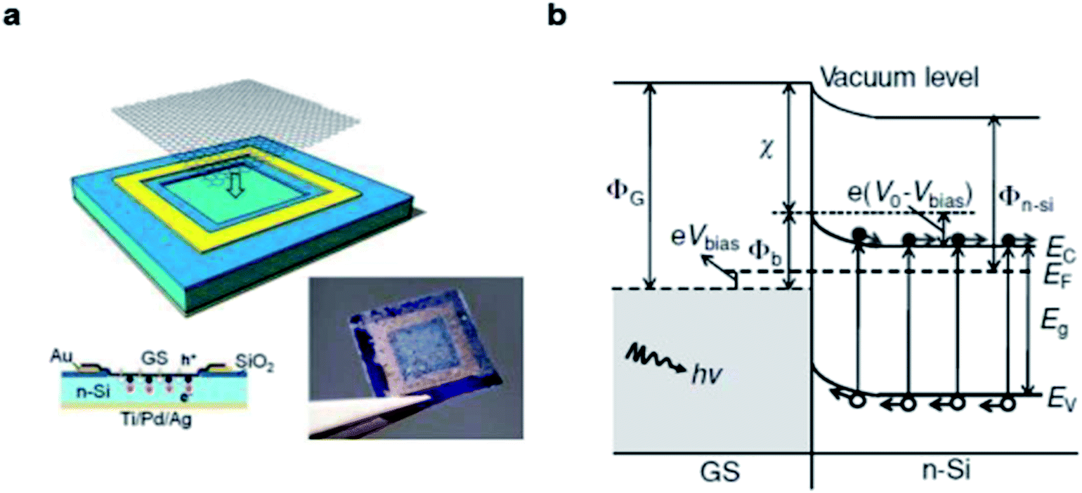 | ||
| Fig. 1 Characterizations of the graphene/n-Si Schottky junction. (a) Schematic illustration of the device configuration. (b) Energy diagram of the forward-biased graphene/n-Si Schottky junction upon illumination. Reproduced from23 with permission from Wiley. | ||
Open-circuit voltage (VOC), short-circuit current (ISC), filling factor (FF) and PCE of the solar cells are the main parameters to evaluate the performance of solar cells. All of them can be obtained from light J–V curves when the devices are tested with a solar simulator under AM 1.5 conditions. When the graphene/Si solar cell is open-circuited, the separation of photon-generated carriers will create VOC. When the solar cell is short-circuited, the extracted photogenerated carriers can transit through the external circuit, generating ISC. At V = VOC, these two currents will cancel each other and result in a zero net current. The PCE (η) of a solar cell is defined as the incident power which is converted to electricity and it can be expressed as below:
 | (1) |
 | (2) |
The non-linear dark J–V characteristics of the graphene/Si solar cells can be described by the formula as follows:39
 | (3) |
![[thin space (1/6-em)]](https://www.rsc.org/images/entities/char_2009.gif) J–V curve.
J–V curve.
According to Schottky–Mott mode, the mental with work function (Φmetal) higher than the electron affinity (χe) of the a certain semiconductor can create a Schottky barrier height,41ΦSBH = Φmetal − χe, which is helpful to produce a relatively large built-in filed to block the recombination of holes and electrons. Similarly, the junction barrier height between graphene and silicon also observes the rules. The barrier height ΦSBH can be obtained by the thermal emission theory:42
 | (4) |
4. The optimization of graphene/Si solar cells
The PCE of the first graphene/Si solar cell is only about 1.5%, far below the requirements for industrial application.23 The poor performance of the solar cells can be attributed to: (1) the pristine single-layer graphene has low work function (∼4.4 eV) and large sheet resistance (a few kohms).20 The low work function can decrease the barrier height, which will lower the built-in electric field and prevent electron–hole pairs separating,43 while the large sheet resistance can lead to large series resistance. (2) The absorbed photon number is reduced by the planar Si wafers which is 30–40% for visible light (350–800 nm).44 After graphene/Si solar cells was reported in 2010,23 lots of methods are developed to tune the work function and conductivity of graphene and the reflectance Si wafers, such as chemical doping,45–50 increasing layer number of graphene51,52 and introducing an interlayer,53–59 all of which can help to optimize the performance of solar cells significantly.4.1 Optimization of the work function and conductivity of graphene
 | ||
| Fig. 2 (a) Schematic illustration of the vapor doping process. The device was exposed to the SOCl2 (or HNO3) vapor for a few seconds and chlorine (nitrate) anions were doped on the films. (b) Scheme of the doping mechanism. (c) J–V characteristics of the solar cell before (red curve) and after (black) infiltration of dilute SOCl2. (d) Light J–V curves and PCE of solar cells before and after volatile oxidant treatment. (e) The band schematics at the MLG/Si interface before and after doping. Reproduced from46 and48 with permission from The Royal Society of Chemistry. | ||
Similar to HNO3, SOCl2 and H2O2 can also lead to the improved performance of solar cells. Four volatile oxidants HNO3, SOCl2, HCl, and H2O2 were employed by Cui et al. to dope the graphene films in graphene/Si solar cells.48 They placed the assembled graphene/Si solar cells above a vial containing HNO3 (65 wt%), SOCl2 (99.5 wt%), HCl (36 wt%), or H2O2 (30 wt%) for 1 min. It has been shown that the PCE could be remarkably enhanced after being treated by either of the four volatile oxidants. The PCE enhancement of the volatile oxidant-treated cells are primarily contributed by the improvement in FF and VOC. Among all the four volatile oxidants, the PCE enhanced by SOCl2 doping showed the best improvement (Fig. 2d). A solar cell with an initial PCE of 2.58% (VOC = 412.10 mV, JSC = 17.65 mA cm−2, FF = 35.42%) could be increased to 5.95% (VOC = 547.78 mV, JSC = 17.92 mA cm−2, FF = 60.64%) after SOCl2 doping treatment (Fig. 2c). They also investigated the stability of the volatile oxidant-treated cells by keeping them in ambient conditions for 8 days. Due to the volatilization of the volatile oxidant, the PCE of the volatile oxidant treated cells decreased with storage time in the air, and the results also showed that solar cells treated by SOCl2 and HCl have relatively better stability than that of HNO3 and H2O2 ones.
In addition to the volatile oxidants, doping with organic polymer dopant TFSA is also an effect way to improve the performance of graphene/Si solar cells. Miao et al. reported that TFSA could increase the conductivity of graphene significantly by p-doping.45 They demonstrated that the PCE of the device doping with TFSA was increased to 8.6% from the original (undoped) PCE of 1.9% and the JSC increased from 14.2 to 25.3 mA cm−2, VOC increased from 0.43 to 0.54 V, respectively. Fig. 3a and b notes that p-type doping can increase the work function of graphene, which will lead to an improvement of ΦSBH, creating a larger potential drop across the depletion width and allowing a more efficient of electrons and holes separation and collection. Due to the p-type doping effect, the enhanced work function of the graphene therefore leads to an decrease the sheet resistance and improvement of the barrier height in graphene/n-Si junction.61 The electrical and optical properties of monolayer graphene after TFSA doping were also investigated by Lai et al.62 The results showed that doping with TFSA can efficiently lower the sheet resistance of graphene because the resistance decreased from 1200 Ω cm2 to 300 Ω cm2 rapidly, and the UV-visible transmittance spectra also presented that the TFSA preserved graphene's optical properties without any significant reduction that single layer graphene still remained extremely high transmittance after chemical doping (Fig. 3c), all of which make it possible to fabricate graphene–Si solar cells with superior electrical–optical properties.
 | ||
| Fig. 3 (a) J–V characteristics in the semi-logarithmic scale. (b) Amplified J–V characteristics of graphene/n-Si diodes. (c) The transmittance spectra of graphene. (a and b) Reproduced from45 with permission from The American Chemical Society (c) reproduced from62 with permission from IEEE Xplore. | ||
In addition to volatile oxidants and TFSA, several groups also attempted to improve the PCE of graphene/Si solar cells by metal nanoparticles (NPs) such as Au, Pt.49,60,63,64 Introducing nanoparticles not only improves the work function and decreases the sheet resistance of graphene, but can possibly increase the light absorption and PCE of the devices.65 For example, Kim and the coworkers deposited Au layer on graphene by radio frequency sputtering and annealed in nitrogen atmosphere to gain Au NP-doped graphene–Si solar cells.64 As displayed in Fig. 4a, the discrete spherical nanoparticles are uniformly distributed on the graphene surface. In the XPS spectra, shown in Fig. 4b, indicating Au NPs are successfully doped into graphene. The PCE was increased from 3.52% to 7.51% after doping of Au nanoparticles. It was further enhanced to 10.69% by co-doping it with TFSA.
 | ||
| Fig. 4 (a) SEM image of the surface of Au NPs/TFSA-doped graphene. The scale bar indicates 200 nm. (b) XPS spectra of graphene layers with and without Au NPs/TFSA dopants. (c) VOC, (d) JSC and FF, (e) PCE as functions of the Au thickness for both Au NPs/MLG/Si and Au NPs/FLG/Si solar cells. (f) Schematic diagrams of Pt-GWF/n-Si solar cell. (a and b) Reproduced from64 with permission from The Royal Society of Chemistry. (c–e) Reproduced from60 with permission from American Institute of Physics. (f) Reproduced from63 with permission from The Royal Society of Chemistry. | ||
Liu et al. also reported a structure of Au nanoparticles/graphene/Si solar cells by incorporating Au nanoparticles onto the graphene layers to improve the device performance.49 Different with Kim et al., they deposited Au thin layer with various thickness onto the monolayer graphene (MLG) and few-layer graphene (FLG), then annealed under nitrogen flow to gain Au NPs with different sizes. Fig. 4c showing that the VOC increases monotonically with Au thickness for the two batches of devices, and the VOC of the solar cells with multilayer graphene (0.40–0.45 V) is much higher than that of single layer devices (0.26–0.42 V), which is in good agreement with the previous works in which the VOC difference is attributed to the increased work function of graphene with more layers.51 Unlike VOC, the value of JSC is found to exhibit a first-rise then decrease behavior of which the critical Au thickness was 9 nm, and FF showed a similar tendency as JSC (Fig. 4d). Due to the increased VOC, JSC, and FF after incorporating Au nanoparticles, a maximum PCE of 7.34% has been obtained for the Au nanoparticles/multilayer graphene/Si cells when the Au thickness is 9 nm, which is more than three times of the original value (Fig. 4e). In this work, Au-doping gives rise to an enhanced built-in electric field and thus an improved VOC in the solar cell, meanwhile, the enhanced electrical conductivity of graphene and the reduced RS of cell lead to a higher FF and JSC. This work provides a route for developing stable, and highly efficient graphene/Si solar cells.
Kang et al. developed an effective and practical method to deposit Pt nanoparticles on graphene woven fabrics (GWF) to improve the performance of graphene/silicon solar cells.63 (Fig. 4f) The deposition of Pt NPs increased the work function of GWF and also reduced the sheet resistance of GWF. The increased work function of GWF resulted in an enhanced built-in electric field and thus an improved VOC, whereas the enhanced conductivity led to a higher JSC, thereby improving the PCE of graphene/silicon solar cells. To further enhance the PCE of the solar cells, they also coated solid electrolyte (HNO3 + PVA) onto the Pt NPs–GWF/n-Si solar cells which serves as photoelectron chemical channel, and the PCE was improved to 10.02%. In comparison, the efficiency of the solar cell that was only coated with solid electrolyte (without Pt NPs deposition) was 7.51%. The results suggest that the deposition of Pt NPs can improve the performance of the GWF/n-Si solar cells significantly. But it is worth noting that Pt is expensive compared with other metals, so it is necessary to find cheaper metal nanoparticles that can enhance the efficiency of graphene/Si solar cells in the future.
The effect of the number of graphene layers on the performance of graphene/n-Si solar cells were investigated by Li et al.51 They found that the VOC improved monotonically when the layer number of graphene increased (Fig. 5b). The reason is that the graphene work function could be tuned by its layer number, leading to improved barrier height of graphene/n-Si Schottky junction. Fig. 5 shows that with increasing graphene layer number, JSC first linear increases when the layer number of graphene less than 4, and then decreases when it further increases. They explained that the sheet resistance (RS) decreases when the layer number is less than 4, and then it has an opposite trend when the layer number more than 4. In addition, with the increase of layer number, the transmission of graphene reduced. In consideration of the sheet resistance and the transmittance, the 4-layer graphene solar cells exhibit the best performance.
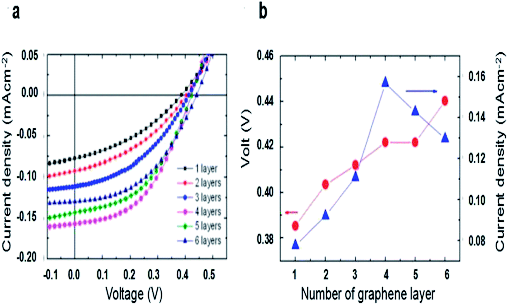 | ||
| Fig. 5 (a) Current–voltage curves of solar cells based on graphene with 1, 2, 3, 4, 5, and 6 layers under illumination of 730 nm LED (2 mW cm−2). (b) The open-circuit voltage and short-circuit current of solar cells measured as functions of the number of graphene layers. (a and b) Reproduced from51 with permission from American Institute of Physics. | ||
Ihm et al. reported that the layer number-dependent trend is reversed for graphene/p-Si solar cells.52 They found that VOC decreased as the layer number of graphene increased. Similar in graphene/n-Si junction solar cells, when the layers increase, the work functions of graphene shows a sequential increase accordingly. And in the graphene/p-Si cell, ΦB = χSi − ΦG, so the barrier height of graphene/p-Si reduces, while improves that of graphene/n-Si junction solar cells. Jiao et al. fabricated PMMA/bilayer graphene/CNWs-Si solar cell with a maximum PCE of 8.9%.66 A PMMA/few-layer graphene could be achieved by a layer-by-layer (LBL) transfer method67,68 and poly(methylmethacrylate) (PMMA) film was kept after transferring graphene, serving as an efficient antireflection layer. As the layer number of graphene increased from 1 to 4, the transmittance decreased from 96% to 87% in the visible range, while the RS declined from 458 to 183 Ω cm2. When the RS (337 Ω cm2) and transmittance (94.5% at 550 nm) had the best tradeoff with 2 layers, the optimal PCE of 8.9% was attained with JSC, VOC and FF values of 29.1 mA cm−2, 0.44 V, and 69.8%, respectively. When the layer number increased to 4, the FF improved to 71.8% due to low RS, and the JSC decreased to 25.1 mA cm−2 as a result of low transmittance, the efficiency declined to 7.6% (Table 1).
| Method | Cell structure | PCE (%) | Year | Ref. |
|---|---|---|---|---|
| Original | Graphene/n-Si | 1.65 | 2010 | 23 |
| Chemical doping | HNO3/graphene/n-Si | 4.35 | 2011 | 47 |
| SOCl2/graphene/n-Si | 5.95 | 2013 | 48 | |
| TFSA/graphene/n-Si | 8.6 | 2012 | 45 | |
| Nanoparticle doping | Au NPs/graphene/n-Si | 7.34 | 2014 | 49 |
| Pt NPs/GWF/n-Si | 10.02 | 2016 | 63 | |
| Layer number | 4 layer graphene/n-Si | 1.48 | 2014 | 51 |
| Light trapping | SOCl2/graphene/SiNW array | 2.86 | 2011 | 81 |
| HNO3/graphene/SiPA | 3.55 | 2011 | 75 | |
| AuCl3/graphene/SiHA | 10.4 | 2013 | 84 | |
| Antireflection layer | HNO3/TiO2/graphene/n-Si | 14.5 | 2013 | 44 |
| PMMA/bilayer graphene/CNWs/Si | 8.9 | 2016 | 66 | |
| HNO3/PMMA/graphene/n-Si | 13.34 | 2016 | 85 | |
| MgF2/ZnS/graphene/n-Si | 14.6 | 2018 | 87 | |
| Interface engineering | Graphene/SiO2/n-Si | 12.4 | 2015 | 53 |
| HNO3/4-layer graphene/P3HT/CH3–Si | 10.56 | 2013 | 59 | |
| Au NPs/HNO3/graphene/h-BN/n-Si | 10.93 | 2016 | 58 |
4.2 Optimization of the reflectivity of silicon
 | ||
| Fig. 6 Schematics diagrams of (a) graphene/planar Si and (b) graphene/SiNW junctions. (c) Schematic illustration of the graphene/SiHA Schottky junction solar cell. (d) Top-view SEM image of the graphene/SiHA device. (e) Photovoltaic characteristics and (f) EQE spectra of the graphene/SiHA Schottky junction solar cells with various hole depths. (a and b) Reproduced from81 with permission from The American Chemical Society. (c–f) Reproduced from84 with permission from The Royal Society of Chemistry. | ||
Shi et al. introduced TiO2 as an antireflection layer, the structure can be illustrated as sandwich structure with TiO2 layer on the top, graphene in the middle, n-Si substrate at the bottom (Fig. 7a).44 The efficiency of the control cell without TiO2 antireflection layer is 8.9% after HNO3 doping. Then TiO2 colloidal solution was spin-coated on the window of graphene/Si solar cells to form a smooth and thin film. After coating TiO2, the reflectance was lowered to about 10% in the visible region (500–800 nm). Consequently, the JSC was increased significantly by 30% (from 23.9 to 32.5 mA cm−2). The resulting HNO3 doped-TiO2–graphene–Si cell showed a VOC of 0.60 V, a FF of 73%, and an efficiency of 14.1% (Fig. 7c). Here, HNO3 doping mainly improve the VOC and FF, while TiO2 coating significantly enhance the JSC. After optimized with both routes, the power conversion efficiency of both of graphene/Si solar cell reached 14.1%. The device stability was studied after storing the solar cell for about 20 days in the ambient air. The results showed that the JSC remained unchanged, VOC dropped from 0.60 to 0.45 V and the FF reduced from 73% to 45%, resulting in a degradation of cell efficiency (from 14.1% to 6.5%). So it can be deduced that doping by volatile acid is indeed not stable and cell degradation occurs after loss of acid and doping effect. However, the antireflection effect by TiO2 coating was excellent since the JSC remained unchanged about 32 mA cm−2 during the storage period. After that, they treated it by HNO3 vapor again, the VOC returned from 0.45 to 0.6 V, FF to 72%. The efficiency of the re-doping solar cell can recover to 14.5%, slightly higher than that before.
 | ||
| Fig. 7 (a) Illustration of the TiO2/graphene/Si structure (left) and cross-sectional SEM image showing a uniform TiO2 coating (thickness of ∼65 nm) on top of the graphene–Si cell. (b) Schematic illustration of color graphene/Si heterojunction solar cells with double layer-MgF2/ZnS films. Inset shows the SEM image of the Ag grid mesh. (c) J–V characteristics of an as fabricated graphene–Si solar cell, after HNO3 vapor doping, and after TiO2 coating (combined with HNO3 doping), respectively. (d) Transmittance spectra of PMMA-removed and PMMA-coated (2000 rpm) graphene. The inset is a typical Raman spectrum of graphene on SiO2/Si. Transmittance values at 550 nm are 96.0% and 97.4% for PMMA-coated and PMMA-removed samples, respectively. (e) J–V spectra of the devices with different structural colors measured under AM1.5, 100 mW cm−2. J–V spectra of the devices without coating and with optimized anti-reflection coating were also presented for comparison. (a and c) Reproduced from104 with permission from The American Chemical Society. (b and e) Reproduced from87 with permission from Elsevier. (d) Reproduced from85 with permission from The Royal Society of Chemistry. | ||
Gan et al. demonstrated a novel way of PMMA film as an antireflection layer on a graphene/silicon solar cell.85 Traditionally, PMMA protective coating was regarded as a protection layer during graphene transfer process, and is usually removed after transfer process.91,92 In this work, the PMMA was remained on the graphene film acting as an anti-reflection layer. And the Fig. 7d shows that the transmittance at 550 nm measured was 96.0% with PMMA coatings. With the PMMA-coating and HNO3 doping, the PCE reached up to 13.34%. They also compared the antireflection effect of TiO2 with that of PMMA. The result showed that the efficiency of TiO2-coated graphene/Si solar cells are significantly inferior to those of PMMA-coated graphene/Si solar cells.
Ding et al. fabricated multi-color graphene/Si solar cells by taking advantage of the combination of MgF2/ZnS anti-reflection coating and graphene (Fig. 7b).87 ZnS owns the maximum refractive index nearly 2.5 while MgF2 owns the minimum refractive index of 1.4.93,94 Therefore, the double layer MgF2/ZnS films can serve as efficient antireflection layers for solar cells. Meanwhile, they can enabled the graphene/Si solar cells with high color saturation. In this work, Ding et al. deposited MgF2/ZnS in sequence onto the graphene/Si solar cell by thermal evaporation. Different structural colors can be achieved by carefully tuning the thickness of the films. And the coated graphene/Si solar cells exhibited respectable power conversion efficiency in the range of 10.7–13.2%. With the optimized MgF2/ZnS antireflection coating, PCE of the device can reach up to 14.6% (Fig. 7e). Their work demonstrates the great potential to fabricate colorful graphene/Si solar cells for future high-efficiency, low-cost and designable PV panels.
4.3 Interface engineering
The PCE of the graphene/Si solar cells can reach up to 10% after reflectivity optimization of silicon, but the efficiency is still much lower than the commercial silicon solar cells based on p–n junction, which is mainly restricted by the strong re-combination of carriers along the interface due to the low barrier height. One solution to this problem is to introduce a passivation dielectric film between graphene and Si, thereby forming a metal-insulator-semiconductor (MIS) structure.95,96 In a MIS solar cell, the additional insulating film can reduce the carrier recombination by suppressing diffusion of electrons from n-Si to graphene, and help the holes transfer to the graphene layer through tunnelling processes. Both mechanisms lead to improved VOC and PCE of solar cells.The best insulating layer materials include SiO2,53,54 MoS2,55 Al2O3,56 graphene oxide (GO),57 h-BN,58 3-hexylthiophene (P3HT).59 Several groups have demonstrated that the interface of the graphene/Si heterojunction play an important role in high efficient photoelectronic devices.53–59
Song et al. inserted SiO2 as an electron blocking layer by exposing the substrate in air to allow the native oxide to regrow and layer thicknesses were optimized for achieving the best performance for graphene/Si solar cells.53 In the conventional Si wafer pretreatment, the native silicon oxide was usually completely etched before the graphene films were transferred. However, it has been demonstrated that leaving the silicon exposed to air for some time can allow a moderately thick oxide to regrow,97,98 yielding improved performance. To systematically study the effect of oxide thickness on the performance of the graphene/Si solar cells, the devices were left in air for varied duration before transferring graphene. The results showed that with the increasing oxide thickness from 5 Å to 15 Å, the efficiency can be improved from 7.9% to 12.4%. VOC and FF were both improved further if the device left in air longer before transfer. For devices with 15 Å oxide, VOC increased to 0.59 V and the FF increased to 0.74. Furthermore, TiO2 antireflective coating (ARC) and AuCl3 doping were also applied to the device, the overall efficiency can reach up to 15.6%.
P3HT organic layer were introduced by Xie et al. and Zhang et al. as an interfacial layer, and in their work, P3HT was inserted into the graphene–Si interface as an electron blocking layer, preventing electrons diffusion from n-Si to the graphene, minimizing the dark saturation current and a large leakage current.59 P3HT layer was spin-coated on Si within the window area and the thickness of the P3HT layer was carefully controlled by adjusting the solution concentration. With the increasing of the P3HT thickness, the PCE improved from 4.24% with 0 nm-thick P3HT layer to 9.70% with a 10 nm-thick P3HT layer. Further increase of the P3HT thickness to 40 nm would result in an obvious performance degradation. Supplemented with the by doping and optimization of the graphene layer number, a PCE of 10.56% was achieved.
Meng et al. introduced a few-layer h-BN between graphene and n-Si to improve the performance of the solar cells.58 As shown in Fig. 8a, the few-layer h-BN and the CVD-grown few-layer graphene were successively transferred onto the patterned substrate by LBL transfer process. After introducing the h-BN layer, the VOC and PCE were increased from 0.412 to 0.474 V and from 3.75% to 4.40%, respectively in pristine cells (Fig. 8b). They explained that the h-BN can not only act as an effective electron-blocking/hole-transporting layer, but also has suitable band alignment with Si, and thus the interface recombination was suppressed and the open circuit voltage was significantly increased (Fig. 8c and d). In order to avoid the interface contamination and defects arising from the LBL process, they also transferred the directly grown graphene/h-BN heterostructure onto the graphene/h-BN/Si solar cell by one step method.99 A maximum efficiency of 10.93% was achieved for the graphene/h-BN/Si solar cells by combining the directly grown graphene/h-BN heterostructures with co-doping of graphene with Au nanoparticles and HNO3.
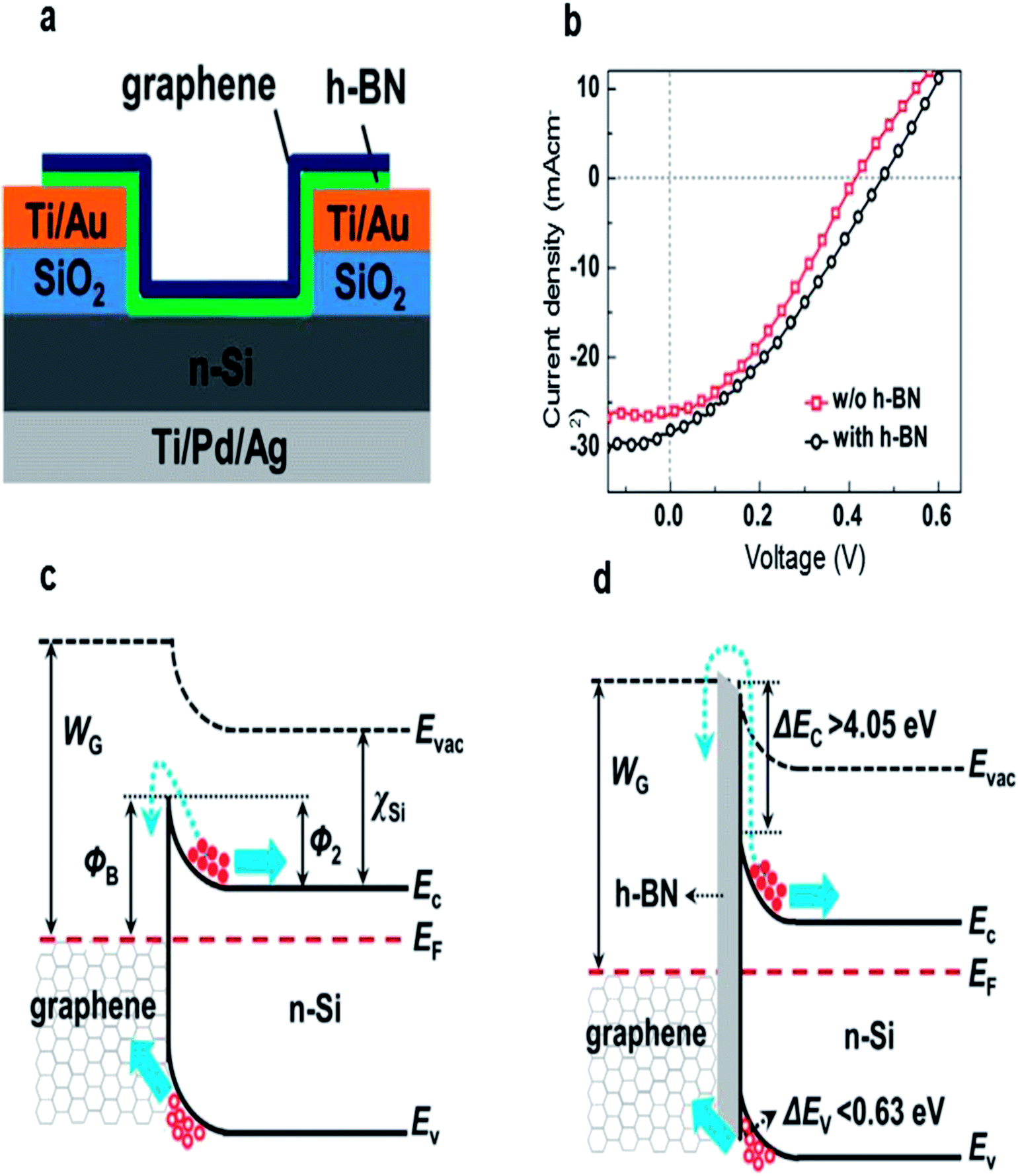 | ||
| Fig. 8 (a) Schematic illustration of graphene/h-BN/Si solar cells. (b) Illuminated J–V characteristics of the graphene/Si solar cells with and without an h-BN interlayer. (c and d) Energy band diagrams of the graphene/Si Schottky junction solar cells without and with an h-BN electron blocking layer. Reproduced from 58 with permission from Elsevier. | ||
Ma et al. demonstrate the fabrication of high efficiency graphene/MoS2/Si Schottky barrier solar cells with MoS2 interlayers.55 The inserted MoS2 layers function as hole transport layer to facilitate the separation of electron–hole pairs as well as electron blocking layer to suppress the recombination at graphene/silicon interfaces. By optimizing the thickness of MoS2 layers, a high photovoltaic conversion efficiency of 15.8% was achieved in graphene/MoS2/Si solar cells, which is a new record reported so far.
5. Conclusions, challenges and prospects
In this article, we briefly reviewed the optimization approaches of the graphene/Si Schottky solar cells in recent years. These approaches could be categorized as optimization of (1) the work function and conductivity of graphene, (2) the reflectivity of silicon, (3) passivation and energy band engineering of the graphene/Si interface. Assisted with these approaches, the PCE has increased from 1.5% to 15.8% in less than a decade. In spite of the rapid progress in this field, there are still some issues need to be addressed.(1) Till now, different approaches have been tried to improve the efficiency of the solar cells, such as chemical doping of graphene, passivation and band-engineering of the graphene/Si interface, introduction of antireflection layer or nano/microstructures to improve the light harvest, the graphene layer number controlling. Among them, chemical doping has been recognized as the most effective method to optimize the performance of the solar cells. Although many doping dopants have been introduced, the stability of solar cells is still a serious challenge due to the instability of the doping methods. Cui et al. presented a significant high-stability single-walled carbon nanotube (SWNT)/Si solar cells with a PCE over 11% after 10 months of exposure to ambient conditions.100 Jia et al. demonstrated CNT (carbon nanotube)-oxide–Si cells with a PDMS anti-reflection layer, and the efficiency showed a slight drop from 10.9% to 9.1% for 20 days in air.101 Yang et al. reported a new structure of graphene–Si solar cells by introducing a graphene oxide (GO) interlayer to engineer the graphene–Si interface for improving device performance, the graphene/GO/Si solar cell retains 95% of its original level after storing in the open air for one week.102 Rehman et al. inserted an Al2O3 interlayer between the Si and graphene to suppress the surface charge recombination at the interface, and the efficiency of solar cell was not degraded after 9 months period exposed in ambient air.103 So, a high stability of materials such as carbon nanotube can be used for a long-term stability of the solar cell. In addition, exploring new structure of the solar cells, for example, introduce an interlayer to engineer a graphene–Si interface to form a metal insulator semiconductor (MIS) structure may also be an important direction in this field.
(2) The PCE of the graphene/Si solar cells has reached up to 15.8% in just a few years, but it is still lower than that of commercial Si p–n junction solar cells. Due to the limitation of low electrical conductivity and low work function of graphene, the active area of the solar cell is relatively small (<10 mm2) in current research. Xie et al. and Zhang et al. demonstrated the device performance with various device areas from 4 to 100 mm2, they found that with the increasing device area, the PCE decreased from 10.56% to 3.62%,59 similarly, Shi et al. also reported that the PCE of graphene/Si solar cells decreased from 14.5% to 10.6% when the active area was increased from 4.7 mm2 to 14.5 mm2,104 all these results show that there is a close relationship between the active area and PCE. With a larger size of active area, the collection efficient of photogenerated charge carriers would be lower because of the low conductivity of the graphene layer. In order the improve the conductivity of the graphene layer, Suhail et al. introduced with grid electrode to the conventional window-based device structure,105 which could provide a low resistance contact to the graphene layer, and it might also help to improve the efficiency of carrier collection. So a fine metal electrode design should be adopted on the front to facilitate carrier collection through the entire device area.
(3) It is known that graphene is transferred on the Si substrate to form the Schottky junction, but graphene is easy to be cracked and torn, and copper particles residual may remain on the graphene film after the wet etching,91,106 all the defects and impurities at the graphene/Si interface can serve as short-circuit channels and lead to current leakage. Predictably, the current leakage will be more obvious at a larger device area. And large area of graphene is therefore a critical factor influencing the collection efficiency. In this regard, more matured production and transfer skills should be developed to decrease the defects and impurities arisen in the wet transfer process, and it is also a reliable method to grow graphene directly on semiconductor surface to get less structural defects and uniform film of graphene.107
Conflicts of interest
There are no conflicts to declare.Acknowledgements
This project was supported by National Science Foundation of China (No. 11574014).References
- M. A. Green, Energy Policy, 2000, 28, 989–998 CrossRef.
- S. Ashraf, R. Su, J. Akhtar, H. M. Siddiqi and A. El-Shafei, Dyes Pigm., 2018, 150, 347–353 CrossRef CAS.
- S. Mathew, A. Yella, P. Gao, R. Humphry-Baker, B. F. Curchod, N. Ashari-Astani, I. Tavernelli, U. Rothlisberger, M. K. Nazeeruddin and M. Gratzel, Nat. Chem., 2014, 6, 242–247 CrossRef CAS.
- W. S. Yang, B. W. Park, E. H. Jung, N. J. Jeon, Y. C. Kim, D. U. Lee, S. S. Shin, J. Seo, E. K. Kim, J. H. Noh and S. I. Seok, Science, 2017, 356, 1376–1379 CrossRef CAS.
- K. Yoshikawa, W. Yoshida, T. Irie, H. Kawasaki, K. Konishi, H. Ishibashi, T. Asatani, D. Adachi, M. Kanematsu, H. Uzu and K. Yamamoto, Sol. Energy Mater. Sol. Cells, 2017, 173, 37–42 CrossRef CAS.
- G. A. Kachurin, I. E. Tyschenko and L. I. Fedina, Nucl. Instrum. Methods Phys. Res., 1992, 68, 323–330 CrossRef.
- T. Warabisako, T. Uematsu, S. Muramatsu, K. Tsutsui, H. Ohtsuka, Y. Nagata and M. Sakamoto, Sol. Energy Mater. Sol. Cells, 1997, 48, 137–143 CrossRef CAS.
- W. Di and K. Jani, Nanoscale, 2013, 5, 10108–10126 RSC.
- Y. Ye, L. Dai, P. C. Wu, C. Liu, T. Sun, R. M. Ma and G. G. Qin, Nanotechnology, 2009, 20, 375202 CrossRef CAS.
- S. B. Photodiodes, Metal-semiconductor Schottky barrier junctions and their applications, Plenum Press, 1984 Search PubMed.
- D. W. Kim, Y. J. Sung, J. W. Park and G. Y. Yeom, Thin Solid Films, 2001, 398, 87–92 CrossRef.
- J. Li, H. Chen and J. Xue, J. Photonics Energy, 2014, 4, 040990 CrossRef.
- K. S. Novoselov, A. K. Geim, S. V. Morozov, D. Jiang, Y. Zhang, S. V. Dubonos, I. V. Grigorieva and A. A. Firsov, Science, 2004, 306, 666–669 CrossRef CAS.
- B. Partoens and F. M. Peeters, Phys. Rev. B: Condens. Matter Mater. Phys., 2006, 74, 075404 CrossRef.
- L. A. Falkovsky, J. Phys.: Conf. Ser., 2008, 129, 012004 CrossRef.
- R. R. Nair, P. Blake and A. N. Grigorenko, et al. , Science, 2008, 320, 1308 CrossRef CAS PubMed.
- F. Bonaccorso, Z. Sun, T. Hasan and A. C. Ferrari, Nat. Photonics, 2010, 4, 611–622 CrossRef CAS.
- A. K. Geim and K. S. Novoselov, Nat. Mater., 2007, 6, 183–191 CrossRef CAS.
- J. Wu, M. Agrawal, H. A. Becerril, Z. Bao, Z. Liu, Y. Chen and P. Peumans, ACS Nano, 2010, 4, 43–48 CrossRef CAS.
- T.-H. Han, Y. Lee, M.-R. Choi, S.-H. Woo, S.-H. Bae, B. H. Hong, J.-H. Ahn and T.-W. Lee, Nat. Photonics, 2012, 6, 105–110 CrossRef CAS.
- Z. Fan, B. Liu, X. Liu, Z. Li, H. Wang, S. Yang and J. Wang, Electrochim. Acta, 2013, 109, 602–608 CrossRef CAS.
- E. W. Hill, A. Vijayaragahvan and K. Novoselov, IEEE Sens. J., 2011, 11, 3161–3170 CAS.
- X. Li, H. Zhu, K. Wang, A. Cao, J. Wei, C. Li, Y. Jia, Z. Li, X. Li and D. Wu, Adv. Mater., 2010, 22, 2743–2748 CrossRef CAS.
- X. Wang, A. Linjie Zhi and K. Müllen, Nano Lett., 2008, 8, 323 CrossRef CAS.
- K. S. Kim, Y. Zhao, H. Jang, S. Y. Lee, J. M. Kim, K. S. Kim, J. H. Ahn, P. Kim, J. Y. Choi and B. H. Hong, Nature, 2009, 457, 706–710 CrossRef CAS.
- Z. Liu, Q. Liu, Y. Huang, Y. Ma, S. Yin, X. Zhang, W. Sun and Y. Chen, Adv. Mater., 2008, 20, 3924–3930 CrossRef CAS.
- S. Bae, H. Kim, Y. Lee, X. Xu, J. S. Park, Y. Zheng, J. Balakrishnan, T. Lei, H. R. Kim, Y. I. Song, Y. J. Kim, K. S. Kim, B. Ozyilmaz, J. H. Ahn, B. H. Hong and S. Iijima, Nat. Nanotechnol., 2010, 5, 574–578 CrossRef CAS.
- S. Pang, Y. Hernandez, X. Feng and K. Mullen, Adv. Mater., 2011, 23, 2779–2795 CrossRef CAS.
- P. Avouris, Nano Lett., 2010, 10, 4285–4294 CrossRef CAS.
- Y. J. Yu, Y. Zhao, S. Ryu, L. E. Brus, K. S. Kim and P. Kim, Nano Lett., 2009, 9, 3430–3434 CrossRef CAS.
- W. Chen, S. Chen, D. C. Qi, X. Y. Gao and A. T. Wee, J. Am. Chem. Soc., 2007, 129, 10418–10422 CrossRef CAS PubMed.
- C. Lee, X. Wei, J. W. Kysar and J. Hone, Science, 2008, 321, 385–388 CrossRef CAS.
- Ç. Ö. Girit, J. C. Meyer, R. Erni, M. D. Rossell, C. Kisielowski, Y. Li, C. H. Park, M. F. Crommie, M. L. Cohen and S. G. Louie, Science, 2009, 323, 1705–1708 CrossRef.
- G. Fiori, F. Bonaccorso, G. Iannaccone, T. Palacios, D. Neumaier, A. Seabaugh, S. K. Banerjee and L. Colombo, Nat. Nanotechnol., 2014, 9, 768–779 CrossRef CAS.
- X. Wang, H. You, F. Liu, M. Li, L. Wan, S. Li, Q. Li, Y. Xu, R. Tian, Z. Yu, D. Xiang and J. Cheng, Chem. Vap. Deposition, 2009, 15, 53–56 CrossRef CAS.
- A. Di Bartolomeo, Phys. Rep., 2016, 606, 1–58 CrossRef CAS.
- M.-Y. Li, C.-H. Chen, Y. Shi and L.-J. Li, Mater. Today, 2016, 19, 322–335 CrossRef CAS.
- H. Zhong, K. Xu, Z. Liu, G. Xu, L. Shi, Y. Fan, J. Wang, G. Ren and H. Yang, J. Appl. Phys., 2014, 115, 013701 CrossRef.
- S. M. Sze, IEEE J. Quantum Electron., 1981, 15, 1438 Search PubMed.
- D. Sinha and J. U. Lee, Nano Lett., 2014, 14, 4660–4664 CrossRef CAS.
- H. Yang, J. Heo, S. Park, H. J. Song, D. H. Seo, K. E. Byun, P. Kim, I. Yoo, H. J. Chung and K. Kim, Science, 2012, 336, 1140 CrossRef CAS.
- S. Tongay, M. Lemaitre, X. Miao, B. Gila, B. R. Appleton and A. F. Hebard, Phys. Rev. X, 2012, 2, 011002 Search PubMed.
- Y. Lin, X. Li, D. Xie, T. Feng, Y. Chen, R. Song, H. Tian, T. Ren, M. Zhong, K. Wang and H. Zhu, Energy Environ. Sci., 2013, 6, 108–115 RSC.
- E. Shi, L. Zhang, Z. Li, P. Li, Y. Shang, Y. Jia, J. Wei, K. Wang, H. Zhu, D. Wu, S. Zhang and A. Cao, Sci. Rep., 2012, 2, 884 CrossRef.
- X. Miao, S. Tongay, M. K. Petterson, K. Berke, A. G. Rinzler, B. R. Appleton and A. F. Hebard, Nano Lett., 2012, 12, 2745–2750 CrossRef CAS.
- X. Li, D. Xie, H. Park, M. Zhu, T. H. Zeng, K. Wang, J. Wei, D. Wu, J. Kong and H. Zhu, Nanoscale, 2013, 5, 1945–1948 RSC.
- T. Feng, D. Xie, Y. Lin, H. Zhao, Y. Chen, H. Tian, T. Ren, X. Li, Z. Li, K. Wang, D. Wu and H. Zhu, Nanoscale, 2012, 4, 2130–2133 RSC.
- T. Cui, R. Lv, Z.-H. Huang, S. Chen, Z. Zhang, X. Gan, Y. Jia, X. Li, K. Wang, D. Wu and F. Kang, J. Mater. Chem. A, 2013, 1, 5736 RSC.
- X. Liu, X. W. Zhang, Z. G. Yin, J. H. Meng, H. L. Gao, L. Q. Zhang, Y. J. Zhao and H. L. Wang, Appl. Phys. Lett., 2014, 105, 183901 CrossRef.
- Y. Jia, A. Cao, X. Bai, Z. Li, L. Zhang, N. Guo, J. Wei, K. Wang, H. Zhu, D. Wu and P. M. Ajayan, Nano Lett., 2011, 11, 1901–1905 CrossRef CAS.
- Y. F. Li, W. Yang, Z. Q. Tu, Z. C. Liu, F. Yang, L. Q. Zhang and R. Hatakeyama, Appl. Phys. Lett., 2014, 104, 043903 CrossRef.
- K. Ihm, J. T. Lim, K.-J. Lee, J. W. Kwon, T.-H. Kang, S. Chung, S. Bae, J. H. Kim, B. H. Hong and G. Y. Yeom, Appl. Phys. Lett., 2010, 97, 032113 CrossRef.
- Y. Song, X. Li, C. Mackin, X. Zhang, W. Fang, T. Palacios, H. Zhu and J. Kong, Nano Lett., 2015, 15, 2104–2110 CrossRef CAS.
- Y. Jia, P. Li, X. Gui, J. Wei, K. Wang, H. Zhu, D. Wu, L. Zhang, A. Cao and Y. Xu, Appl. Phys. Lett., 2011, 98, 133115 CrossRef.
- J. Ma, H. Bai, W. Zhao, Y. Yuan and K. Zhang, Sol. Energy, 2018, 160, 76–84 CrossRef CAS.
- M. A. Rehman, I. Akhtar, W. Choi, K. Akbar, A. Farooq, S. Hussain, M. A. Shehzad, S.-H. Chun, J. Jung and Y. Seo, Carbon, 2018, 132, 157–164 CrossRef.
- L. Yang, X. Yu, M. Xu, H. Chen and D. Yang, J. Mater. Chem. A, 2014, 2, 16877–16883 RSC.
- J.-H. Meng, X. Liu, X.-W. Zhang, Y. Zhang, H.-L. Wang, Z.-G. Yin, Y.-Z. Zhang, H. Liu, J.-B. You and H. Yan, Nano Energy, 2016, 28, 44–50 CrossRef CAS.
- C. Xie, X. Zhang, Y. Wu, X. Zhang, X. Zhang, Y. Wang, W. Zhang, P. Gao, Y. Han and J. Jie, J. Mater. Chem. A, 2013, 1, 8567 RSC.
- X. Liu, X. W. Zhang, J. H. Meng, Z. G. Yin, L. Q. Zhang, H. L. Wang and J. L. Wu, Appl. Phys. Lett., 2015, 106, 233901 CrossRef.
- K. K. Kim, A. Reina, Y. Shi, H. Park, L. J. Li, Y. H. Lee and J. Kong, Nanotechnology, 2010, 21, 285205 CrossRef PubMed.
- Y. C. Lai, B. S. Wu, S. C. Yu, P. C. Yu and G. C. Chi, in 2013 Ieee 39th Photovoltaic Specialists Conference, 2013, pp. 2436–2438 Search PubMed.
- Z. Kang, X. Tan, X. Li, T. Xiao, L. Zhang, J. Lao, X. Li, S. Cheng, D. Xie and H. Zhu, Phys. Chem. Chem. Phys., 2016, 18, 1992–1997 RSC.
- J. H. Kim, D. H. Shin, H. S. Lee, C. W. Jang, J. M. Kim, S. W. Seo, S. Kim and S.-H. Choi, J. Mater. Chem. C, 2017, 5, 9005–9011 RSC.
- X. Liu, X. W. Zhang, J. H. Meng, H. L. Wang, Z. G. Yin, J. L. Wu and H. L. Gao, Nanotechnology, 2014, 25, 365602 CrossRef CAS PubMed.
- T. Jiao, D. Wei, X. Song, T. Sun, J. Yang, L. Yu, Y. Feng, W. Sun, W. Wei, H. Shi, C. Hu and C. Du, RSC Adv., 2016, 6, 10175–10179 RSC.
- Y. Wang, S. W. Tong, X. F. Xu, B. Ozyilmaz and K. P. Loh, Adv. Mater., 2011, 23, 1514–1518 CrossRef CAS PubMed.
- J. Kang, D. Shin, S. Bae and B. H. Hong, Nanoscale, 2012, 4, 5527–5537 RSC.
- C.-H. Sun, P. Jiang and B. Jiang, Appl. Phys. Lett., 2008, 92, 061112 CrossRef.
- Y. Zeng, X. Fan, J. Chen, S. He, Z. Yi, X. Ye and Y. Yi, Superlattices Microstruct., 2018, 117, 144–154 CrossRef CAS.
- T. Aho, M. Guina, F. Elsehrawy, F. Cappelluti, M. Raappana, A. Tukiainen, A. Alam, I. Vartiainen, M. Kuittinen and T. Niemi, Opt. Express, 2018, 26, A331–A340 CrossRef CAS PubMed.
- H. Dai, J. Sun, Z. Li, X. Yu, J. Zhao, H. Fang and Z. Zhu, Trans. Indian Inst. Met., 2018, 71, 1681–1686 CrossRef CAS.
- X. Jiang, P. Zhang, J. Zhang, J. Wang, G. Li, X. Fang, L. Yang and X. Chen, Nanoscale Res. Lett., 2018, 13, 53 CrossRef PubMed.
- H. C. Chen, C. C. Lin, H. W. Han, Y. L. Tsai, C. H. Chang, H. W. Wang, M. A. Tsai, H. C. Kuo and P. Yu, Opt. Express, 2011, 19(suppl 5), A1141 CrossRef CAS PubMed.
- T. Feng, D. Xie, Y. Lin, Y. Zang, T. Ren, R. Song, H. Zhao, H. Tian, X. Li, H. Zhu and L. Liu, Appl. Phys. Lett., 2011, 99, 233505 CrossRef.
- J.-T. Lin, C.-C. Lai, C.-T. Lee, Y.-Y. Hu, K.-Y. Ho and S. W. Haga, IEEE J. Photovolt., 2018, 8, 669–675 Search PubMed.
- E. Garnett and P. Yang, Nano Lett., 2010, 10, 1082 CrossRef CAS PubMed.
- E. C. Garnett and P. Yang, J. Am. Chem. Soc., 2008, 130, 9224–9225 CrossRef CAS PubMed.
- S. K. Srivastava, D. Kumar, S. W. Schmitt, K. N. Sood, S. H. Christiansen and P. K. Singh, Nanotechnology, 2014, 25, 175601 CrossRef PubMed.
- H. Jansen, M. De Boer, R. Legtenberg and M. Elwenspoek, J. Micromech. Microeng., 1999, 5, 115–120 CrossRef.
- G. Fan, H. Zhu, K. Wang, J. Wei, X. Li, Q. Shu, N. Guo and D. Wu, ACS Appl. Mater. Interfaces, 2011, 3, 721–725 CrossRef CAS PubMed.
- Y. P. Hsu, S. J. Chang, Y. K. Su, J. K. Sheu, C. H. Kuo, C. S. Chang and S. C. Shei, Opt. Mater., 2005, 27, 1171–1174 CrossRef CAS.
- H. Jansen, M. D. Boer, H. Wensink, B. Kloeck and M. Elwenspoek, Microelectron. J., 2001, 32, 769–777 CrossRef CAS.
- C. Xie, X. Zhang, K. Ruan, Z. Shao, S. S. Dhaliwal, L. Wang, Q. Zhang, X. Zhang and J. Jie, J. Mater. Chem. A, 2013, 1, 15348 RSC.
- X. Gan, R. Lv, H. Zhu, L.-P. Ma, X. Wang, Z. Zhang, Z.-H. Huang, H. Zhu, W. Ren, M. Terrones and F. Kang, J. Mater. Chem. A, 2016, 4, 13795–13802 RSC.
- X. Zhang, H. Ye, B. Xiao, L. Yan, H. Lv and B. Jiang, J. Phys. Chem. C, 2010, 114, 19979–19983 CrossRef CAS.
- K. Ding, X. Zhang, L. Ning, Z. Shao, P. Xiao, A. Ho-Baillie, X. Zhang and J. Jie, Nano Energy, 2018, 46, 257–265 CrossRef CAS.
- L. Lancellotti, E. Bobeico, A. Castaldo, P. Delli Veneri, E. Lago and N. Lisi, Thin Solid Films, 2018, 646, 21–27 CrossRef CAS.
- H. K. Raut, V. A. Ganesh, A. S. Nair and S. Ramakrishna, Energy Environ. Sci., 2011, 4, 3779 RSC.
- R. B. Pettit, C. J. Brinker and C. S. Ashley, Sol. Cells, 1985, 15, 267–278 CrossRef CAS.
- X. Liang, B. A. Sperling, I. Calizo, G. Cheng, C. A. Hacker, Q. Zhang, Y. Obeng, K. Yan, H. Peng and Q. Li, ACS Nano, 2011, 5, 9144–9153 CrossRef PubMed.
- X. Li, Y. Zhu, W. Cai, M. Borysiak, B. Han, D. Chen, R. D. Piner, L. Colombo and R. S. Ruoff, Nano Lett., 2009, 9, 4359 CrossRef CAS PubMed.
- G. R. Olbright, N. Peyghambarian, H. M. Gibbs, H. A. Macleod and F. Van Milligen, Appl. Phys. Lett., 1984, 45, 1031–1033 CrossRef CAS.
- Z. Chen, P. Sana, J. Salami and A. Rohatgi, IEEE Trans. Electron Devices, 2002, 40, 1161–1165 CrossRef.
- J. Bae, H. Kim, X. M. Zhang, C. H. Dang, Y. Zhang, Y. J. Choi, A. Nurmikko and Z. L. Wang, Nanotechnology, 2010, 21, 095502 CrossRef PubMed.
- C. H. Lin, Nanoscale Res. Lett., 2012, 7, 343 CrossRef PubMed.
- M. Morita, T. Ohmi, E. Hasegawa, M. Kawakami and M. Ohwada, J. Appl. Phys., 1990, 68, 1272–1281 CrossRef CAS.
- M. Morita, T. Ohmi, E. Hasegawa, M. Kawakami and K. Suma, Appl. Phys. Lett., 1989, 55, 562–564 CrossRef CAS.
- J. H. Meng, X. W. Zhang, H. L. Wang, X. B. Ren, C. H. Jin, Z. G. Yin, X. Liu and H. Liu, Nanoscale, 2015, 7, 16046–16053 RSC.
- K. Cui, A. S. Anisimov, T. Chiba, S. Fujii, H. Kataura, A. G. Nasibulin, S. Chiashi, E. I. Kauppinen and S. Maruyama, J. Mater. Chem. A, 2014, 2, 11311–11318 RSC.
- Y. Jia, P. Li, X. Gui, J. Wei, K. Wang, H. Zhu, D. Wu, L. Zhang, A. Cao and Y. Xu, Appl. Phys. Lett., 2011, 98, 239 Search PubMed.
- L. Yang, X. Yu, M. Xu, H. Chen and D. Yang, J. Mater. Chem. A, 2014, 2, 16877–16883 RSC.
- M. A. Rehman, I. Akhtar, W. Choi, K. Akbar, A. Farooq, S. Hussain, M. A. Shehzad, S. H. Chun, J. Jung and Y. Seo, Carbon, 2018, 132, 157–164 CrossRef.
- E. Shi, H. Li, L. Yang, L. Zhang, Z. Li, P. Li, Y. Shang, S. Wu, X. Li, J. Wei, K. Wang, H. Zhu, D. Wu, Y. Fang and A. Cao, Nano Lett., 2013, 13, 1776–1781 CrossRef CAS PubMed.
- A. Suhail, G. Pan, D. Jenkins and K. Islam, Carbon, 2018, 129, 520–526 CrossRef CAS.
- M. Her, R. Beams and L. Novotny, Phys. Lett. A, 2013, 377, 1455–1458 CrossRef CAS.
- M. F. Bhopal, K. Akbar, M. A. Rehman, D. w. Lee, A. u. Rehman, Y. Seo, S.-H. Chun and S. H. Lee, Carbon, 2017, 125, 56–62 CrossRef CAS.
| This journal is © The Royal Society of Chemistry 2019 |