
 Open Access Article
 This Open Access Article is licensed under a
 Creative Commons Attribution 3.0 Unported Licence
Crystal recombination control by using Ce doped in mesoporous TiO2 for efficient perovskite solar cells†
Honglin Lu,
Jia Zhuang *,
Zhu Ma*,
Weiya Zhou,
Haoran Xia,
Zheng Xiao,
Hua Zhang and
Haimin Li
*,
Zhu Ma*,
Weiya Zhou,
Haoran Xia,
Zheng Xiao,
Hua Zhang and
Haimin Li
The Center of New Energy Materials and Technology, School of Materials Science and Engineering, Southwest Petroleum University, Chengdu 610500, P. R. China. E-mail: zj-656@163.com; deve198509@163.com; Fax: +86 02883033286; Tel: +86 13550396098 Tel: +86 13880863057
First published on 9th January 2019
Abstract
Efficient electron transport layers (ETLs) are the crucial issue for electron transport and hole blocking in organic–inorganic hybrid perovskite solar cells (PSCs). To date, most of the reported effective ETLs have comprised TiO2, which exhibits limited electron mobility and numerous defect states and restricts the enhancement of the performance of PSCs. Hence, the investigation of effective tactics for improving the electronic properties of TiO2 is critical for the fabrication of high-efficiency devices. In this study, a cerium doping method was adopted in mesoporous TiO2, which was prepared via a traditional one-step hydrothermal process, to improve its electron transport properties by recombining nanocrystals and optimizing the negative flat band potential of TiO2. Continuous, aligned and regulated recombined crystals of mesoporous TiO2 were obtained with optimized pathways of electron transport from the ETL to the FTO layer. Moreover, a small amount of Ti4+ ions was replaced by Ce4+ ions in the TiO2 lattice, which led to deformation of the TiO2 lattice and influenced the growth process of TiO2 grains. With an optimized mole proportion of Ce element in the TiO2 precursor, the power conversion efficiency (PCE) of perovskite solar cells was typically boosted to 17.75% in comparison with 15.92% in the case of undoped TiO2.
Introduction
In recent years, numerous works have focused on organic–inorganic hybrid perovskite solar cells (PSCs) owing to their strong photovoltaic properties and low cost of manufacture. Their photoelectric conversion efficiency (PCE) has increased enormously from 3.8% in 2009 to 23.3% in 2018.1–3 Owing to the untiring efforts of researchers, PSCs will have great potential as replacements for silicon-based solar cells. In typical PSCs, a perovskite absorber layer, either with or without a mesoporous scaffold, is sandwiched between the electron transport layer (ETL) and the hole transport layer (HTL).4,5 The ETL has a significant function in transporting electrons and blocking holes.6–8To date, various metal oxide films have been employed as ETLs, such as TiO2, ZnO, SnO2, CeO2, BaSnO3, Nb2O5, SrTiO3 and In2S3,9–17 of which TiO2 has been the most frequently used material. In comparison with compact TiO2 (c-TiO2), mesoporous TiO2 (m-TiO2) is usually used as a scaffold over c-TiO2 to enhance the electron transport, light absorption and environmental stability of PSCs.18,19 At present, most high-efficiency PSCs are based on m-TiO2. However, m-TiO2 suffers from many problems, such as the surface and internal oxygen vacancies in m-TiO2, low conductivity, and multiple defect state densities, which lead to the loss of performance in PSCs.20,21
Surface passivation is considered to be an efficient method of boosting electron transport in silicon-based solar cells and PSCs from the absorption layer to the electrodes or ETLs and reducing electron recombination, which further increases the PCE of the device. Many groups have focused on the interfacial engineering of ETLs to increase the PCE of cells. For instance, Jia et al. introduced CsI as an interfacial modification layer between MAPbI3 and m-TiO2, which could improve the surface morphology of m-TiO2, reduce the work function of TiO2, and reduce the surface defect density.22 Zheng et al. reported an easy strategy whereby the deposition of both aminocaproic acid and caproic acid between mesoporous TiO2 and an MAPbI3 layer achieved a significant increase in PCE, which could contribute to the accelerated extraction and transfer of electrons via interfacial modification.23 Although the surface passivation of m-TiO2 can notably increase the PCE of devices, this additional modification process is contrary to the requirement for a simple fabrication process for the industrialization of PSCs. Therefore, it is important to search for a cost-effective and easy manufacturing method for processing high-quality and efficient m-TiO2 ETLs.
Recently, an ion doping method has been used to replace this additional modification process and moreover improve the optoelectronic properties of m-TiO2 ETLs. At present, many researchers have reported the ion doping of ETLs to increase the PCE of devices. For example, in the case of tungsten-doped TiO2 it was demonstrated that the conduction band (CB) of TiO2 was shifted downward, which is beneficial for electron transport because of the optimized energy level matching between the lowest unoccupied molecular orbital (LUMO) of an MAPbI3 layer and the CB of TiO2.24 Su et al. demonstrated that niobium (Nb)-doped TiO2 was manufactured via a one-step spin-coating process and the PCE of a cell increased from 14.9% to 16.3%, which was attributed to the increased charge density and conductivity of the TiO2 ETL.25 Chen et al. reported that in PSCs based on lithium-doped TiO2 the density of electron trap states can be increased.26 Moreover, aluminum, cesium and cadmium have been doped into TiO2 ETLs to improve the performance of PSCs by controlling the carrier dynamics in TiO2.27–29 Thus far, the aim of doping ions into TiO2 has mainly been to enhance the electronic properties of ETLs, which is mainly attributed to the high conductivity of the doped metal itself and the improved alignment of energy levels. However, few researchers have proposed schemes for the improvement of electronic properties by optimizing the morphology of TiO2 films by ion doping, which promotes electron transport in ETLs and decreases electron recombination.
In this study, a crystal recombination phenomenon was observed after cerium element was doped into mesoporous TiO2, which was prepared using a one-step hydrothermal method. The regulated crystal recombination provided optimized transport pathways for the extraction and transport of electrons. PSCs exhibited a maximum PCE of 17.75% with an increased open-circuit voltage (VOC), short-circuit current density (JSC), and fill factor (FF) in comparison with undoped cells. The overall enhancement in performance was ascribed to the excellent electronic properties of the ETL.
Results and discussion
Fig. 1a shows a schematic flow chart of the fabrication process of mesoporous TiO2. Compact TiO2 was prepared by spin coating, and mesoporous TiO2 was fabricated by a hydrothermal method. SEM images of mesoporous TiO2 and mesoporous TiO2 doped with 2% Ce are presented in Fig. 1b and c, respectively. As seen in Fig. 1b and c, we obtained nanoparticle-shaped TiO2 by a hydrothermal method, whereby mesoporous TiO2 doped with 2% Ce exhibited recombined crystalline grains with a greater diameter and a smoother nanodruse surface than undoped m-TiO2. The morphology of Ce-doped m-TiO2 promoted the transport and penetration of electrons from the MAPbI3 absorption layer into the mesoporous ETL, which possessed planar and mesoporous characteristics.30,31 Fig. 1d shows the diameter distribution of crystalline grain agglomerates, which further demonstrates that the diameter of crystalline grain agglomerates was larger when 2% Ce ions were doped into mesoporous TiO2.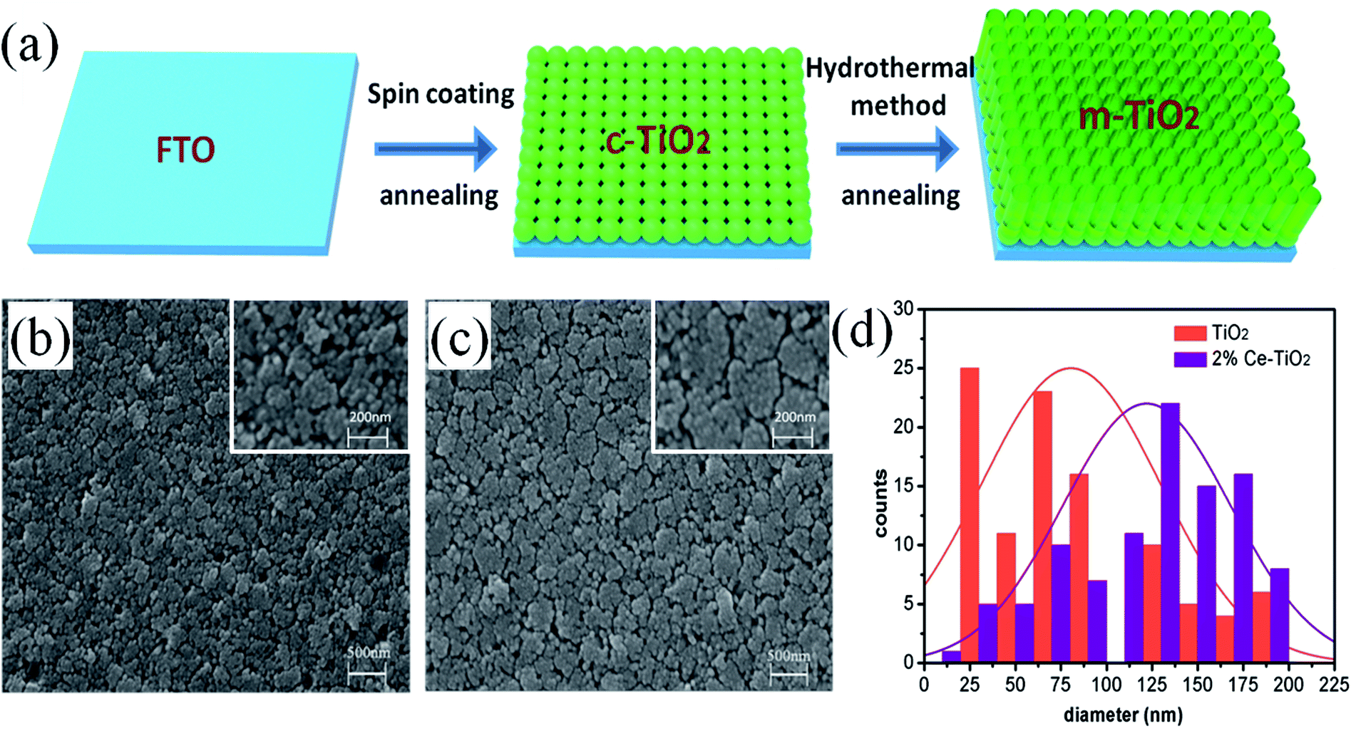 | ||
| Fig. 1 (a) Schematic flow chart of the fabrication of compact TiO2 and mesoporous TiO2, (b) and (c) SEM images of FTO/c-TiO2/m-TiO2 and FTO/c-TiO2/2% Ce-doped m-TiO2, (d) diameters of crystalline grain agglomerates of mesoporous TiO2. | ||
High-resolution transmission electron microscopy (HRTEM) was used to elucidate the reason for the lattice deformation that occurred when 2% Ce was doped into m-TiO2 (Fig. 2a and b). The lattice spacing measured from an HRTEM image was 0.35 nm (inset of Fig. 2a), which corresponded to the (101) crystallographic planes of the anatase form of titanium dioxide. Doping 2% Ce into TiO2 led to lattice deformation and a decrease in the spacing (0.31 nm) between the (101) crystallographic planes of the anatase form of titanium dioxide. This result shows that Ce element penetrated into the TiO2 lattice. Because the ionic radius of Ce4+ ions is greater than that of Ti4+ ions, the extrusion effect of ion replacement caused the lattice spacing to decrease. Fig. 2c illustrates the reason why mesoporous TiO2 doped with 2% Ce had a greater diameter of crystalline grain agglomerates when Ce4+ ions were doped into the TiO2 lattice.32,33 (A study showed that the critical temperature for the valence state from Ce3+ ion to Ce4+ ion is 200 °C. The experimental temperature was 500 °C, indicating that the conversion to valence state is credible.) Ce atoms have higher bond energies than Ti atoms, which could enable substitution doping when Ce4+ ions were doped into the TiO2 lattice.32 The incomplete match between the geometric features of the two elements led to slight deformation and strain in the TiO2 lattice. The greater diameter of recombined crystalline grains of TiO2 nanoparticles that was observed can be attributed to the occurrence of lattice deformation and strain induced by the substitution of larger Ce4+ ions (94 pm) in the positions of Ti4+ ions (68 pm). Lattice deformation caused by substitution doping leads to larger crystal particles, improves the regularity of the crystal structure, decreases the number of irregular holes, and provides more channels and opportunities for electron transport. Frank et al. reported that a decrease in film porosity was beneficial for electron transport in an m-TiO2 film.34 High porosity implies longer electron transport pathways, which indicates that electrons will spend a longer time in the m-TiO2 network before being collected.34,35 This result will cause more electron recombination. m-TiO2 doped with 2% Ce (Fig. 1c) exhibited lower porosity than undoped m-TiO2 (Fig. 1b), which was beneficial for improved electron transport and further increased the PCE of cells.
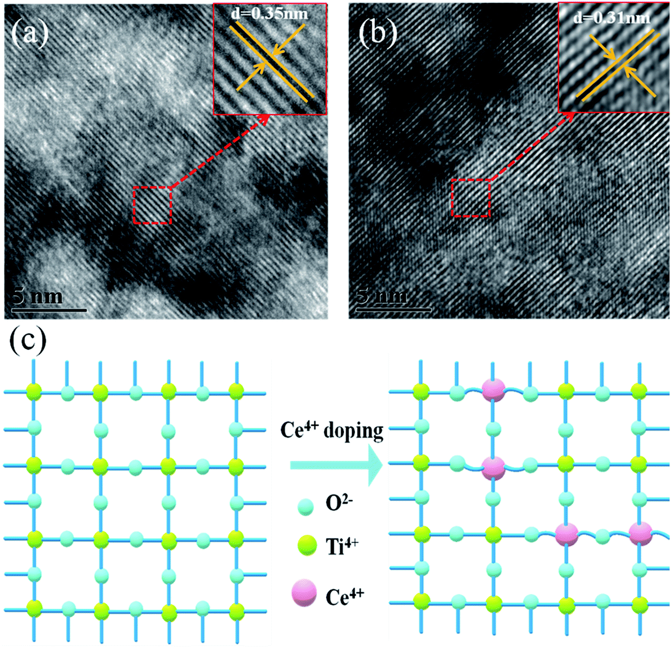 | ||
| Fig. 2 HRTEM images of (a) TiO2 and (b) 2% Ce–TiO2 and (c) 3D model diagram of Ce4+ ions replacing Ti4+ ions in the TiO2 lattice. | ||
Fig. 3a and b show elemental maps of the elemental compositions of undoped and 2% Ce-doped mesoporous TiO2 ETLs, respectively. Tin element originated from FTO glass, and Ti element originated from c-TiO2 and m-TiO2. The presence of cerium element and its uniform distribution demonstrate that Ce was successfully doped into mesoporous TiO2 by doping cerium nitrate pentahydrate into the hydrothermal precursor solution.36 To further confirm the presence and intrinsic effect of cerium element in TiO2, XPS (the carbon peak correction was carried out) was used to determine the chemical compositions and chemical states of undoped mesoporous TiO2 and mesoporous TiO2 doped with 2% Ce.37 The full XPS spectra can be seen in Fig. 3c, which shows the presence of Ti, O, and C elements in undoped mesoporous TiO2 and mesoporous TiO2 doped with 2% Ce. The presence of a C 1s peak is ascribed to adsorbed hydrocarbons on the TiO2 surface. However, the presence of Ce element is not directly indicated in Fig. 3c owing to its low concentration, but its characteristic peak can influence shifts in other peaks of mesoporous TiO2, which could confirm the presence of Ce indirectly. Fig. 3d shows the O 1s peaks of undoped mesoporous TiO2 and mesoporous TiO2 doped with 2% Ce. The Ti 2p spectra in Fig. 3e show that mesoporous TiO2 doped with 2% Ce exhibited a peak shift from 463.4 eV to 463.6 eV in comparison with undoped mesoporous TiO2, i.e., a shift of 0.2 eV. The shifts in the peaks of Ti 2p and O 1s are assigned to the different coordination environments and chemical environments that resulted when Ce4+ ions were doped into mesoporous TiO2. The shifts in the peaks of O 1s and Ti 2p are ascribed to the changes in the charge densities of O and Ti atoms, which could be caused by electron transfer from O 1s orbitals and the 2p orbitals of Ti atoms to Ce 4f orbitals. This result influenced the nucleation and crystallization of m-TiO2 when Ce was doped into m-TiO2, which further improved the morphology of m-TiO2. The characterization via EDS and XPS shows that Ce element was successfully doped into mesoporous TiO2 and was uniformly distributed.
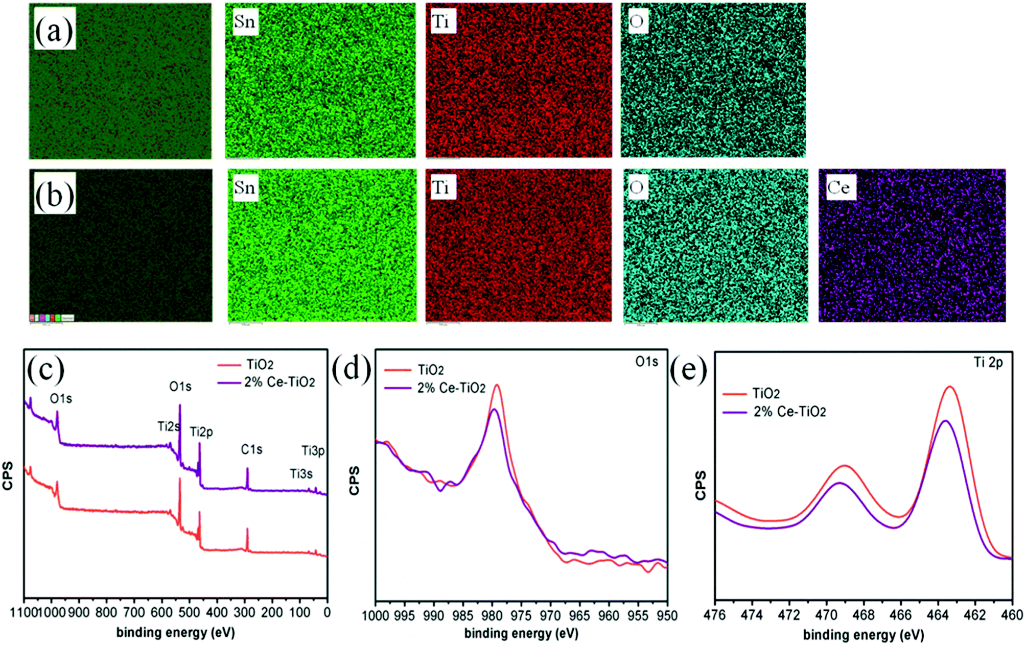 | ||
| Fig. 3 EDX elemental images of (a) FTO/c-TiO2/m-TiO2 and (b) FTO/c-TiO2/2% Ce-doped m-TiO2. XPS measurements of TiO2 and Ce-doped TiO2 mesoporous ETLs: (c) survey spectrum, (d) O 1s spectrum, and (e) Ti 2p spectrum. | ||
Surface SEM images of perovskite films based on undoped mesoporous TiO2 and mesoporous TiO2 doped with 2% Ce are shown in Fig. 4a and b, respectively. When Ce was added to mesoporous TiO2, there was no observable change in the morphology of the perovskite film in comparison with pure mesoporous TiO2. This result shows that the decrease in porosity when Ce was doped into m-TiO2 had no influence on the morphology of the perovskite layer. The perovskite films deposited onto mesoporous TiO2 and Ce-doped mesoporous TiO2 ETL substrates exhibited uniform film-forming abilities, which is important for producing high-efficiency PSCs. Fig. 4c shows the XRD patterns of perovskite thin films deposited on mesoporous TiO2 and 2% Ce-doped mesoporous TiO2 ETLs, which demonstrate that the addition of cerium nitrate did not influence the crystal structure of MAPbI3 and a perovskite film structure was formed. UV-vis absorption spectra (Fig. 4d) show that the CH3NH3PbI3 film based on a 2% Ce-doped TiO2 ETL exhibited a stronger absorption peak due to the CH3NH3PbI3 film within the range of 400–450 nm than the CH3NH3PbI3 film based on an undoped TiO2 ETL, and hence the absorption of visible light by the perovskite layer was further improved. This result further shows the improvement in the PCE of cells after Ce was doped into m-TiO2.
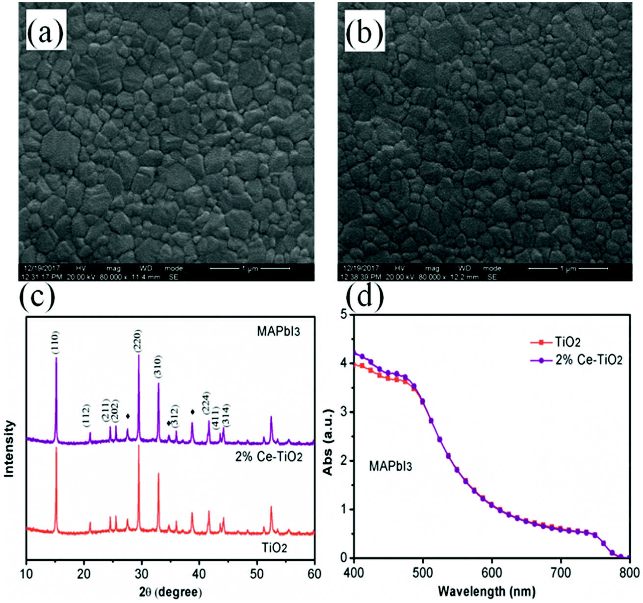 | ||
| Fig. 4 (a) and (b) Top-view SEM images of MAPbI3 films based on mesoporous TiO2 and 2% Ce-doped mesoporous TiO2 ETLs, (c) XRD patterns of MAPbI3 films (♦ represents FTO), and (d) UV-vis absorption spectra of MAPbI3 films based on mesoporous TiO2 and 2% Ce-doped mesoporous TiO2 ETLs. | ||
We manufactured a perovskite solar cell with a cell structure of FTO/c-TiO2 (70 nm)/m-TiO2 (300 nm)/MAPbI3 (500 nm)/spiro-OMeTAD (150 nm)/Ag (100 nm) (Fig. 5a), and a corresponding cross-sectional SEM image is shown in Fig. 5b. The reverse and forward current–voltage (J–V) characteristics of solar cells with and without 2% Ce dopant are shown and summarized in Fig. 5c and Table 1, respectively. The undoped TiO2 cell exhibited a JSC value of 22.80 mA cm−2, a VOC value of 1.020 V, and an FF of 68.50%, with a PCE of 15.92% under reverse scanning (10.11% under forward scanning), whereas the 2% Ce–TiO2 PSC exhibited a PCE of 17.75% (VOC = 1.048 V, JSC = 23.61 mA cm−2, FF = 71.70%) under reverse scanning and a PCE of 13.81% under forward scanning. A decrease in the hysteresis index (to 0.22) was demonstrated for the cell based on 2% Ce-m-TiO2 as the ETL (in comparison with the hysteresis index of 0.36 for the undoped device), which can be ascribed to the improved morphology and increased conductivity of m-TiO2. From Table S1,† we can demonstrate that the JSC and VOC values and FF of Ce-doped cells increased in comparison with the undoped TiO2 cell when the concentration was 1% and 2%. When the dopant concentration was 4%, the JSC and VOC values and FF of the cell declined rapidly. Ce4+ ions doped into m-TiO2 could produce a new impurity energy level, which may help charge capture and separation and may also serve as a recombination center for carriers. Obviously, doping with 4% Ce4+ ions provided m-TiO2 with recombination centers and further exerted a passive influence on the ETL. Therefore, Ce4+ ions were added to increase the JSC and VOC values and FF, which further led to an increase in the PCE at a certain concentration. The statistical distribution of the PCEs of undoped and 2% Ce-doped devices is shown in Fig. 5d, from which the PCEs of cells based on 2% Ce–TiO2 were concentrated around 15% and 16% in comparison with 13% and 14% in the case of undoped devices. The error bars (Fig. 5e, f and S1†) show that the 2% Ce-doped TiO2 cells exhibited higher VOC and JSC values and FFs than the undoped devices, which further illustrates that doping with Ce was effective for improving cell performance.
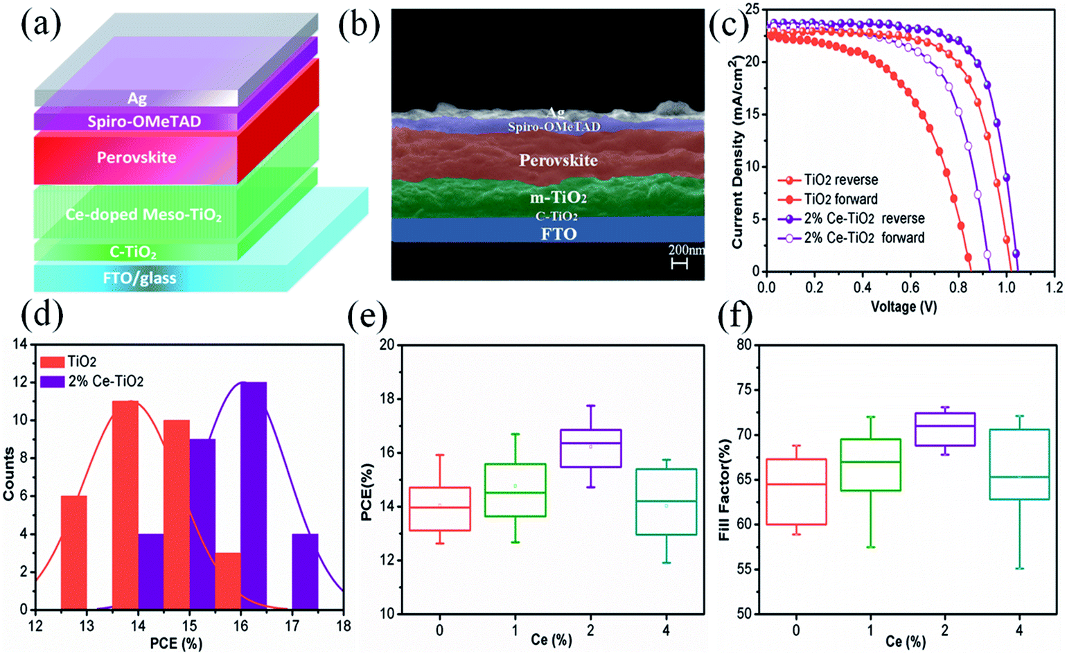 | ||
| Fig. 5 (a) Cell model diagram, (b) cross-sectional SEM image of PSC (FTO/compact TiO2/mesoporous TiO2/CH3NH3PbI3/spiro-OMeTAD/Ag), (c) J–V curves, (d) histogram of PCE, and (e) and (f) error bars of PCE and FF. | ||
| ETL | VOC (V) | JSC (mA cm−2) | FF (%) | PCE (%) | Hysteresis index |
|---|---|---|---|---|---|
| TiO2 reverse | 1.020 | 22.80 | 68.50 | 15.92 | 0.36 |
| TiO2 forward | 0.852 | 22.51 | 52.70 | 10.11 | |
| 2% Ce–TiO2 reverse | 1.048 | 23.61 | 71.70 | 17.75 | 0.22 |
| 2% Ce–TiO2 forward | 0.931 | 23.32 | 63.60 | 13.81 |
In order to get an insight into the relationship between the performance of devices and the properties of Ce-doped mesoporous TiO2, different tactics were used. Fig. 6a shows the UV-vis absorption spectra of undoped and 2% Ce-doped mesoporous TiO2. The absorption spectrum of Ce-doped TiO2 displays a red shift in the band gap (small image in Fig. 6a). The transformed Kubelka–Munk spectra (Fig. 6b) of undoped and 2% Ce-doped TiO2 were recorded to determine the optical band gap. The optical band gap of TiO2 decreased from 3.25 to 3.20 eV when 2% Ce(NO3)3 was doped into the TiO2 precursor solution. This could be attributed to the formation of a Ti–O–Ce bond structure in Ce-doped m-TiO2 owing to the partial substitution of Ti by Ce, which caused the red shift in the band gap of TiO2. The decrease in the band gap can promote an increase in the force of charge injection from the ETL to the FTO glass layer, as shown by the increased JSC value of the device. Fig. 6c shows the Mott–Schottky curves for undoped and 2% Ce-doped mesoporous TiO2. The flat band potential (Vfb) is the external voltage and corresponds to the intercept with the x-axis. A shift in the Vfb value is related to the position of the conduction band of m-TiO2.37 Fig. 6c shows that the Vfb value was negatively shifted from −0.601 V to −0.621 V, whereas the negative shift in the Vfb value implies that the quasi-Fermi level was higher (Fig. 6d). These results further led to an upward shift in the conduction band, which resulted in an increase of 15 mV in the VOC value. The increase of 28 mV observed in the VOC value of the device was much greater than the increase of 15 mV in the VOC value due to the shift in the conduction band, which may be ascribed to the improved morphology and increased conductivity of m-TiO2. Fig. 6e shows the EIS spectra of devices based on undoped and 2% Ce-doped TiO2 as ETLs, which were recorded with an amplitude of 7.5 mV and a measurement frequency ranging from 1 to 100 kHz.38,39 The model in the inset of Fig. 6e shows the fitted equivalent circuit. Table 2 shows the values used for fitting. The arc at high frequencies is attributed to the contact resistance of the interface between the perovskite layer and the ETL, whereas that at low frequencies originated from the recombination resistance (Rrec). The arc at high frequencies shows that doping with 2% Ce had little influence on electron transfer from the perovskite layer and ETL in comparison with the undoped device. The larger semicircle in the curve is generally related to the recombination of electrons. Obviously, the PSC based on mesoporous TiO2 doped with 2% Ce as the ETL exhibited a higher recombination resistance (8535 Ω) than the undoped cell (5420 Ω), which indicated that a lower recombination loss occurred when Ce element was doped into meso-TiO2. This result led to increases in the FF and VOC value of PSCs. Fig. 6f shows a 3D map of electron transport from MAPbI3 to the ETL. The higher PCE of the device based on 2% Ce–TiO2 as the ETL decreased the recombination of electrons owing to the optimized morphology of mesoporous TiO2, the decreased Vfb value and the increased conductivity in comparison with the undoped device.
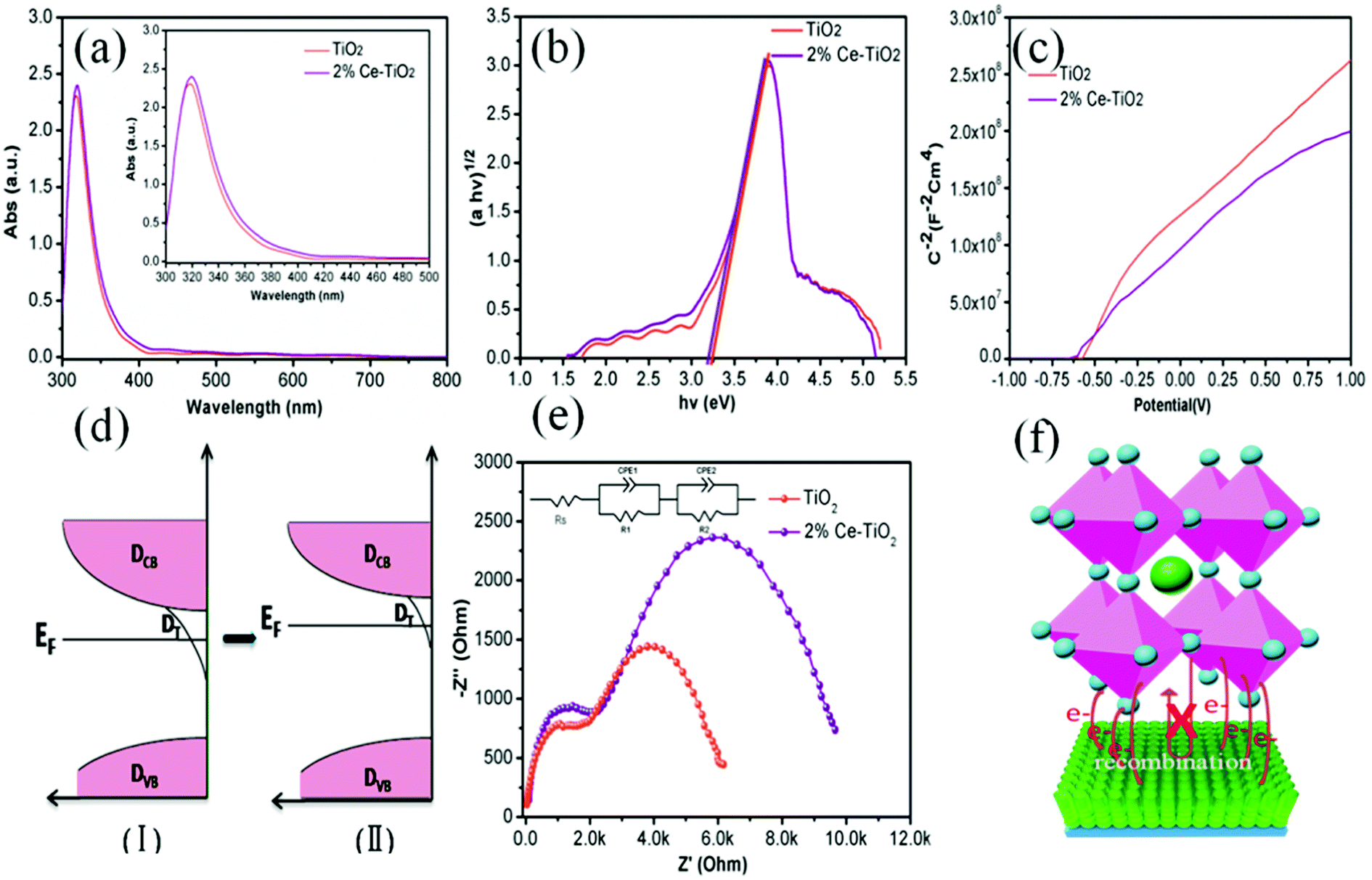 | ||
| Fig. 6 (a) UV-vis absorption spectra of TiO2 and 2% Ce-doped mesoporous TiO2 ETLs, (b) band gap map of TiO2, (c) Mott–Schottky curves for TiO2 and Ce-doped mesoporous TiO2 ETLs, (d) electronic density of states for meso-TiO2 ETLs including the densities of conduction band states (DCB), trap states (DT), and valence band states (DVB) and the decrease in the density of surface trap states due to doping with Ce, (e) EIS spectra of perovskite solar cells based on TiO2 and 2% Ce-doped mesoporous TiO2 as ETLs, and (f) 3D map of electron transport from MAPbI3 to the ETL. | ||
| Sample | Contact resistance (RS/Ω) | Transfer resistance (R1/Ω) | Transfer resistance (R2/Ω) |
|---|---|---|---|
| TiO2 | 29.37 | 1536 | 5420 |
| 2% Ce–TiO2 | 32.43 | 1725 | 8535 |
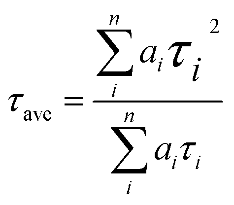
PL (Fig. 7a) and TRPL (Fig. 7b) measurements were used to assess whether charges could be efficiently extracted from the MAPbI3 layer to the mesoporous TiO2 layer.40,41 Fig. 7a shows the steady-state PL spectra of PSCs with the structures FTO/compact TiO2/mesoporous TiO2/perovskite and FTO/compact TiO2/2% Ce-doped mesoporous TiO2/perovskite. From the PL peak at about 775 nm, the CH3NH3PbI3 perovskite film deposited on 2% Ce-doped mesoporous TiO2 exhibited more evident PL quenching in comparison with the pristine mesoporous TiO2 film, which demonstrated an enhanced charge extraction ability. Furthermore, the time constants τe were determined by fitting the TRPL curves (Fig. 7b) to calculate the extraction lifetimes for perovskite layers on mesoporous TiO2 with and without a Ce dopant as the ETL. As a result, the fitted time constants τe were calculated by a biexponential decay function as follows:
 | (1) |
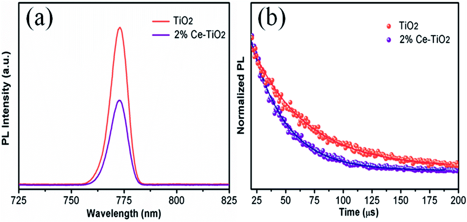 | ||
| Fig. 7 (a) PL and (b) TRPL decay curves for FTO/compact TiO2/mesoporous TiO2/MAPbI3 and FTO/compact TiO2/2% Ce-doped mesoporous TiO2/MAPbI3 films. | ||
The results for the τe values (Table 3) were 37.40 ns for the doped cell and 51.93 ns for the undoped cell, respectively. Thus, the PL decay for the cell based on 2% Ce-doped TiO2 was approximately 27.98% faster in comparison with the PSC based on pristine mesoporous TiO2, which showed that the time taken for electron injection from the perovskite layer to 2% Ce-doped mesoporous TiO2 was shorter. The enhanced electron extraction ability was probably due to the optimized morphology of mesoporous TiO2 and the decrease in the Vfb value, which further resulted in the increase in the PCE of the cell.
| Sample | τave (ns) | τ1 (ns) | Amplitude of τ1 (%) | τ2 (ns) | Amplitude of τ2 (%) |
|---|---|---|---|---|---|
| TiO2 | 51.93 | 1.96 | 0.22 | 51.94 | 99.78 |
| 2% Ce–TiO2 | 37.40 | 2.13 | 0.49 | 37.41 | 99.51 |
We introduced Ce element as an effective doping agent into mesoporous TiO2 to increase the PCE of perovskite solar cells. It was shown that doping of mesoporous TiO2 with Ce improved the optoelectronic properties of the ETL owing to the optimized morphology of mesoporous TiO2 and the decreased Vfb value. The PCE of a cell increased to 17.75% in comparison with the PCE of an undoped device of 15.92%. The increases in the values of JSC and VOC are ascribed to the increase in the force of electron transport from the ETL to the FTO layer and the rise in the quasi-Fermi energy level. The increase in the FF is attributed to the increase in the value of Rrec after Ce was doped into the mesoporous TiO2 ETLs. This study shows that ion doping is an effective strategy for producing high-efficiency perovskite solar cells.
Experimental section
Materials and reagents
Chlorobenzene (99.9%), N,N-dimethylformamide (DMF, 99.9%), titanium isopropoxide (99.999%), and acetonitrile (99.9%) were obtained from Sigma-Aldrich. Cerium(III) nitrate hexahydrate and isopropanol were obtained from Aldrich. 2,2′,7,7′-Tetrakis(N,N′-di-p-methoxyphenylamino)-9,9′-spirobifluorene (spiro-OMeTAD, 99.5%), PbI2 (99.99%), lithium bis(trifluoromethanesulfonyl)imide (Li-TFSI, 99.9%), CH3NH3I (99.5%), and 4-tert-butylpyridine (tBP, 96%) were obtained from Xi'an Polymer Light Technology Company. Glass substrates coated with fluorine-doped tin oxide (FTO) (15 Ω sq−1) were bought from OPV Tech New Energy Co. All the materials and reagents were used without further purification.Solar cell fabrication
The FTO substrates were ultrasonically cleaned with an abstergent, acetone, deionized water, and ethanol for 15 min in each case. The conductive substrates were dried with a nitrogen gun and post-treated with UV–ozone for 15 min. A c-TiO2 layer was coated on the cleaned FTO substrates by spin coating with the titanium precursor solution at 2000 rpm for 30 s. The as-prepared c-TiO2 was post-annealed at 150 °C for 15 min and then heated at 500 °C for 30 min in a muffle furnace. Then, we started to prepare the mesoporous TiO2 precursor solution, and 15 mL hydrochloric acid was mixed with 15 mL deionized water under magnetic stirring for 10 min. Then, 0.75 mL tetra-n-butyl titanate with or without different amounts of cerium(III) nitrate pentahydrate (Ce(NO3)3·5H2O) as a dopant was added to the abovementioned mixed solution, and then the solution was vigorously stirred for 30 min to obtain a clarified solution. Afterwards, the clear solution was transferred into a reaction kettle equipped with compact TiO2/FTO substrates. The sealed reaction kettle was placed in a laboratory oven at 170 °C for 1 h. After the autoclave was cooled to room temperature naturally, the substrate was taken out, rinsed with deionized water and ethanol twice to remove residual reactants, and finally dried with a nitrogen gun and then annealed at 500 °C for 30 min in a muffle furnace. An MAPbI3 layer was spin-coated on c-TiO2/m-TiO2/FTO glass at 3000 rpm for 55 s. CB (80 μL) was washed onto the substrate during the spin-coating method about 10 s before the beginning of the procedure, and the substrate was then annealed at 100 °C for 20 min. An HTL film was manufactured by spin-coating a spiro-OMeTAD solution on a perovskite film at 3000 rpm for 30 s. Finally, an Ag electrode was deposited onto the spiro-OMeTAD layer by a sputtering technique to finish the manufacture of the cell.Characterization
The current–voltage characteristics of perovskite solar cells were determined using an electrochemical workstation under AM 1.5 simulated solar illumination (CEL-S500, Beijing, China). Mott–Schottky plots were recorded by employing an electrochemical workstation with a standard three-electrode configuration with Ag/AgCl as the reference electrode in saturated Na2SO4 and a Pt sheet as the counter electrode in deionized water. The morphology and composition of mesoporous TiO2 films were investigated using a scanning electron microscope (SEM; Zeiss EVOMA15) equipped with an energy-dispersive X-ray spectroscopy (EDX) detector. X-ray diffraction (XRD, DX-2700, Dandong) patterns were recorded from 22° to 58° with Cu Kα radiation (λ = 0.15406 nm) at a scanning rate of 4° min−1. X-ray photoelectron spectroscopy (XPS) measurements were carried out with an X-ray photoelectron spectrometer (Kratos Axis Ultra DLD) with a monochromated Al Kα X-ray source (hν = 1486.6 eV, 200 W). HRTEM images were recorded with a Hitachi HT-7700 transmission electron microscope (Hitachi Limited, Tokyo, Japan) at a voltage of 100 kV. UV-vis absorption spectra were recorded by a UV-vis spectrometer (Varian Cary 5000). Time-resolved photoluminescence (TRPL) spectra were recorded at 765 nm with an Edinburgh Instruments FLS 980 spectrometer with a pulsed diode laser at 485 nm (with an intensity of 0.12 mW cm−2) at a pulse frequency of 1 MHz. Incident photocurrent conversion efficiency (IPCE) spectra were recorded using an IPCE system (PVE 300, Bentham, Inc.) as a function of the wavelength from 300 to 800 nm. The active area of the perovskite solar cells was fixed at 0.16 cm2 using a mask.Conflicts of interest
There are no conflicts to declare.Acknowledgements
The authors gratefully acknowledge the financial support from the Sichuan Science and Technology Program (Grant No. 2018JY0015), the Young Scholars' Development Fund of SWPU (Grant No. 201699010017) and the Scientific Research Starting Project of SWPU (Grant No. 2017QHZ021).References
- A. Kojima, K. Teshima, Y. Shirai and T. Miyasaka, J. Am. Chem. Soc., 2009, 131, 6050–6051 CrossRef CAS PubMed.
- H. Zhou, Q. Chen, G. Li, S. Luo, T. B. Song, H. S. Duan, Z. Hong, J. You, Y. Liu and Y. Yang, Science, 2014, 345, 542–546 CrossRef CAS PubMed.
- https://www.nrel.gov/pv/assets/images/efficiency-chart-20180716.jpg.
- W. S. Yang, J. H. Noh, N. J. Jeon, Y. C. Kim, S. Ryu, J. Seo and S. I. Seok, Science, 2015, 348, 1234–1237 CrossRef CAS PubMed.
- I. C. Smith, E. T. Hoke, D. Solis-Ibarra, M. D. Mcgehee and H. I. Karunadasa, Angew. Chem., Int. Ed., 2014, 53, 11232–11235 CrossRef CAS PubMed.
- Y. Guo, J. Jiang, S. Zuo, F. Shi, J. Tao, Z. Hu, X. Hu, P. Yang and J. Chu, Sol. Energy Mater. Sol. Cells, 2018, 178, 186–192 CrossRef CAS.
- Y. Xiang, J. Yu and J. Zhuang, Sol. Energy Mater. Sol. Cells, 2017, 165, 45–51 CrossRef CAS.
- X. Zhang, T. Wu, X. Xu, L. Zhang, J. Tang, X. He, J. Wu and L. Zhang, Sol. Energy Mater. Sol. Cells, 2018, 178, 65–73 CrossRef CAS.
- H. S. Kim, J. W. Lee, N. Yantara, P. P. Boix, S. A. Kulkarni, S. Mhaisalkar and M. Grätzel, Nano Lett., 2013, 13, 2412–2417 CrossRef CAS PubMed.
- L. Zhang, X. Xu, X. Zhang, J. Tang, L. Zhang, X. He and J. Wu, J. Mater. Chem. C, 2018, 6, 334–341 Search PubMed.
- Z. Ma, H. Lu, F. Zhao, Y. Xiang and J. Zhuang, RSC Adv., 2017, 7, 29357–29363 RSC.
- X. Xu, Z. Xu, J. Tang, X. Zhang, L. Zhang, J. Wu and L. Zhang, Chem. Eng. J., 2018, 351, 391–398 CrossRef CAS.
- S. S. Mali, J. V. Patil, H. Kim and C. K. Hong, Nanoscale, 2018, 10, 8275–8284 RSC.
- L. Zhu, Z. Shao, J. Ye, X. Zhang, X. Pan and S. Dai, Chem. Commun., 2015, 52, 970–973 RSC.
- X. Ling, J. Yuan, D. Liu, Y. Wang, Y. Zhang, S. Chen, H. Wu, F. Jin, F. Wu, G. Shi, X. Tang, J. Zheng, S. F. Liu, Z. Liu and W. Ma, ACS Appl. Mater. Interfaces, 2017, 9, 23181–23188 CrossRef CAS PubMed.
- A. Bera, K. Wu, A. Sheikh, E. Alarousu, O. F. Mohammed and T. Wu, J. Phys. Chem. C, 2014, 118, 28494–28501 CrossRef CAS.
- Y. Hou, X. Chen, S. Yang, Y. Zhong, C. Li, H. Zhao and H. Yang, Nano Energy, 2017, 36, 102–109 CrossRef CAS.
- X. H. Zhang, J. J. Ye, L. Z. Zhu, H. Y. Zheng, X. P. Liu and X. Pan, ACS Appl. Mater. Interfaces, 2016, 8, 35440–35446 CrossRef CAS PubMed.
- A. Sarkar, N. J. Jeon, J. H. Noh and I. S. Sang, J. Phys. Chem. C, 2014, 118, 16688–16693 CrossRef CAS.
- F. Giordano, A. Abate, J. P. C. Baena, M. Saliba, T. Matsui, S. M. Zakeeruddin, M. K. Nazeeruddin, A. Hagfeldt and M. Grätzel, Nat. Commun., 2016, 7, 10379 CrossRef CAS PubMed.
- G. S. Han, Y. H. Song, Y. U. Jin, J. W. Lee, N. G. Park and B. K Kang, ACS Appl. Energy Mater., 2015, 7, 23521–23526 CrossRef CAS PubMed.
- F. Han, J. Luo, B. Zhao, Z. Wan, R. Wang and C. Jia, Electrochim. Acta, 2017, 236, 122–130 CrossRef CAS.
- R. Chen, J. Cao, Y. Wu, X. Jing, B. Wu and N. Zheng, Adv. Mater. Interfaces, 2017, 4, 1700897 CrossRef.
- J. Liu, J. Zhang, G. Yue, X. Lu, Z. Hu and Y. Zhu, Electrochim. Acta, 2016, 195, 143–149 CrossRef CAS.
- B. X. Chen, H. S. Rao, W. G. Li, Y. F. Xu, H. Y. Chen, D. Bi. Kuang and C. Y. Su, J. Mater. Chem. A., 2016, 4, 5647–5653 RSC.
- D. Liu, S. Li, P. Zhang, Y. Wang, R. Zhang, H. Sarvari, F. Wang, J. Wu, Z. Wang and Z. D. Chen, Nano Energy, 2017, 31, 462–468 CrossRef CAS.
- H. Zhang, Y. Lv, Y. Guo, X. Tao, C. Yang and X. Zhou, J. Mater. Sci.: Mater. Electron., 2018, 29, 3759–3766 CrossRef CAS.
- W. Wang, H. Zheng, Y. Liu, J. Sun and L. Gao, J. Nanosci. Nanotechnol., 2016, 16, 12768–12772 CrossRef CAS.
- Y. Li, Y. Guo, Y. Li and X. Zhou, Electrochim. Acta, 2016, 200, 29–36 CrossRef CAS.
- N. Papageorgiou, A. C. Barbé and M. Grätzel, J. Phys. Chem. B, 1998, 102, 4156–4164 CrossRef CAS.
- D. Nanova, A. K. Kast, M. Pfannmöller, C. Müller, L. Veith, I. Wacker, M. Agari, W. Hermes, P. Erk, W. Kowalsky, R. R. Schröder and R. Lovrinčić, Nano Lett., 2014, 14, 2732–2740 CrossRef PubMed.
- M. Asemi and M. Ghanaatshoar, J. Mater. Sci., 2017, 52, 489–503 CrossRef CAS.
- B. Cheng, Y. Xiao, G. Wu and L. Zhang, Appl. Phys. Lett., 2004, 84, 416–418 CrossRef CAS.
- K. D. Benkstein, N. Kopidakis, J. Lagemaat and A. J. Frank, J. Phys. Chem. B, 2003, 107, 7759–7767 CrossRef CAS.
- J. V. D. Lagemaat and A. J. Frank, J. Phys. Chem. B, 2001, 105, 12433–12436 CrossRef.
- Y. Xiang, Z. Ma, J. Zhuang, H. Lu, C. Jia and H. Li, J. Phys. Chem. C, 2017, 121, 20150–20157 CrossRef CAS.
- B. Roose, C. M. Johansen, K. Dupraz, T. Jaouen, P. Aebi, U. Steiner and A. Abate, J. Mater. Chem. A, 2017, 6, 1850–1857 RSC.
- Y. Yan, F. Cai, L. Yang, J. Li, Y. Zhang, F. Qin, C. Xiong, Y. Zhou, D. G. Lidzey and T. Wang, Adv. Mater., 2016, 29, 1604044 CrossRef PubMed.
- L. Chen, G. Wang, L. Niu, Y. Yao, Y. Guan, Y. Cuia and Q. Song, RSC Adv., 2018, 8, 15961–15966 RSC.
- L. Zhang, X. Xu, X. Zhang, J. Tang, L. Zhang, X. He and J. Wu, J. Mater. Chem. C, 2018, 6, 334–341 Search PubMed.
- T. Wen, S. Yang, P. Liu, L. Tang, H. Qiao, X. Chen, X. Yang, Y. Hou and H. Yang, Adv. Energy Mater., 2018, 8, 1703143 CrossRef.
Footnote |
| † Electronic supplementary information (ESI) available. See DOI: 10.1039/c8ra07800a |
| This journal is © The Royal Society of Chemistry 2019 |