
Mixed-halide perovskite for ultrasensitive two-terminal artificial synaptic devices
Haiyang
Yu†
ab,
Jiangdong
Gong†
ab,
Huanhuan
Wei
ab,
Wei
Huang
ab and
Wentao
Xu
 *ab
*ab
aInstitute of Photoelectronic Thin Film Devices and Technology, Nankai University, No. 38 Tongyan Road, Haihe Education Park, Tianjin 300350, People's Republic of China. E-mail: wentao@nankai.edu.cn; bnuch@hotmail.com
bTianjin Key Laboratory of Photoelectronic Thin Film Devices and Technology, No. 38 Tongyan Road, Haihe Education Park, Tianjin 300350, People's Republic of China
First published on 25th March 2019
Abstract
Coexisting-Cooperative-Cognitive (Tri-Co) neuromorphic electronics emulate humankind in order to interact with robotic peers and dynamic environments. To fulfill synaptic functional emulation in a single ultrasensitive and energy-efficient electronic device is of vital importance in this field. This study reports the design and fabrication of two-terminal synaptic devices that are based on mixed halide perovskites (HPs). These devices emulate fundamental synaptic principles by the successive modulation of conductance, for example, excitatory post-synaptic current, paired-pulse facilitation, spike-number dependent plasticity, spike-duration dependent plasticity, spike-voltage dependent plasticity, and spike-rate dependent plasticity. The artificial HP synapses show high sensitivity of 100 mV to external stimuli. These results demonstrate the applicability of the HP synapses in Tri-Co neuromorphic electronics and sensory-motor nervetronics.
Introduction
The brain can remember and process a large amount of information efficiently while consuming relatively little energy.1–3 These superior functions can be ascribed to the highly parallel neural networks of the brain. The human brain contains 1012 neurons, each of which connects to >1000 synapses as information exchange channels in order to communicate with other neurons.4,5 The efficiency and low energy consumption of the brain for information processing have stimulated efforts to develop brain-inspired artificial intelligence devices that can sense and respond to a real environment.6,7Synapses constitute the basic unit of a brain, and synaptic plasticity constitutes the molecular basis of learning and memory. Therefore, the fabrication of a single device that can mimic this synaptic plasticity is an essential step in the construction of an artificial neural network.4,8–10 Traditional silicon complementary metal-oxide-semiconductor (CMOS) technology has been applied to emulate artificial synapses successfully, but each artificial synapse requires ten or more transistors, so they are not practical for realizing a high-density artificial neural network like a biological brain.11,12 Two-terminal and three-terminal device structures have been introduced into artificial synapses.13,14 The change in resistance in two-terminal devices is similar to the change in weights of connections between biological synapses.15 Several synaptic functions, including potentiation/depression of synaptic plasticity, spike-timing dependent plasticity (STDP), and paired-pulse facilitation (PPF) have been mimicked.16–19 Artificial neuromorphic systems that are constructed from synaptic devices have a simple structure and low energy consumption, so, in theory, they could reach a complexity that is approximately equal to a biological brain.6,20,21 These devices provide a feasible path toward building artificial neural networks and Tri-Co electronics.
Halide perovskites (HPs) have remarkable optical and electronic properties, including high light absorption coefficients, tunable bandgaps, long electron–hole diffusion lengths, and long carrier lifetimes.22–25 HPs (i.e., MAPbI3) have been widely used in solar cells, whose power conversion efficiency has exceeded 22%.26–29 However, the development of HP-based solar cells is somewhat hindered; the most relevant here is that its current–voltage curve shows a strong hysteresis, which may result from the ion migration and imbalanced extraction of holes and electrons.30–33 This phenomenon provides a gradual modulation of resistance that can be useful in synaptic electronic devices.
In this study, a two-terminal artificial synapse based on HPs was fabricated by low-temperature solution processes. Artificial synapses based on MAPbClBr2 and MAPbBr3 emulate several synaptic functions, including excitatory post-synaptic current (EPSC), PPF, spike-number dependent plasticity (SNDP), spike-voltage dependent plasticity (SVDP), spike-duration dependent plasticity (SDDP) and spike-rate dependent plasticity (SRDP). These electronic devices are ultrasensitive to external stimuli and energy-efficient.
Experimental section
Material preparation
Methylammonium chloride (MACl) and methylammonium bromide CH3NH3Br (MABr) powders were purchased from Shanghai MaterWin New Materials Co. Ltd., and lead bromide (PbBr2) was purchased from Sigma-Aldrich. All reagents presented here were used without further purification. A 20 wt% solution of MAPbClBr2 was prepared by mixing MACl and PbBr2 at a 1![[thin space (1/6-em)]](https://www.rsc.org/images/entities/char_2009.gif) :1 molar ratio in preblended organic solvents, which consisted of anhydrous N,N-dimethylformamide (DMF) and dimethyl sulfoxide (DMSO) at a 4:1 volume ratio. A 20 wt% solution of MAPbBr3 was prepared by mixing MABr and PbBr2 at a 1:1 molar ratio in the same preblended organic solvents. Both perovskite solutions were stirred at room temperature for >12 h. All the procedures were conducted in a nitrogen-filled glovebox.
:1 molar ratio in preblended organic solvents, which consisted of anhydrous N,N-dimethylformamide (DMF) and dimethyl sulfoxide (DMSO) at a 4:1 volume ratio. A 20 wt% solution of MAPbBr3 was prepared by mixing MABr and PbBr2 at a 1:1 molar ratio in the same preblended organic solvents. Both perovskite solutions were stirred at room temperature for >12 h. All the procedures were conducted in a nitrogen-filled glovebox.
Device fabrication
A heavily As-doped Si substrate was sequentially cleaned by sonication in deionized water, acetone and 2-propanol (IPA) for 15 min each, boiled in IPA, and then treated using UV-ozone for 20 min. To coat the substrates, the as-prepared solution was spin-coated by a consecutive two-step spin-coating procedure in a glovebox filled with N2. First, 50 μL of the HP solution was spin-coated at 1000 rpm for 10 s and 5000 rpm for 30 s then, the solvent treatment was performed at the 10th second during the second step: 70 μL chlorobenzene was quickly dropped onto the spinning substrate. The substrate was then annealed at 130 °C for 30 min to form a well-crystallized thin film. Circular aluminum pads were thermally deposited through a shadow mask onto the HP thin films as the top electrodes.Characterization
X-ray diffraction (XRD) patterns were recorded using a Rigaku Ultima IV instrument. X-ray photoelectron spectroscopy (XPS) was conducted using a Thermo Scientific ESCALAB 250Xi instrument. Atomic force microscopy (AFM) images were recorded using an ARTCAM-130-SIINT microscope. Scanning electronic microscopy (SEM) was performed using a QUANTA FEG 450 field-emission microscope to image the top-view and cross-section morphologies. All electrical measurements were characterized using a Keysight B1500A semiconductor parameter analyzer in an ambient atmosphere.Results and discussion
A neuron consists of a cell body, a large number of dendrites, a long axon, and a synapse, which is a gap of 20–40 nm between the axon terminal of the pre-neuron and the dendrites of the post-neuron (Fig. 1a). To mimic the structure of biological synapses, a two-terminal sandwiched structure (Fig. 1b) was used to implement synaptic electronic devices. Aluminum top electrodes (TEs) emulated the pre-synaptic membrane and highly-doped n-type Si bottom electrodes (BEs) emulated the post-synaptic membrane. The synaptic cleft was emulated by an HP active layer, which transmitted information. MAPbX3 (X: halide(s)) is composed of a cubic lattice of corner-sharing PbX6 octahedrons, each of which has a Pb cation in its center. X anions can migrate through the crystal under vacancy assistance, which is a prerequisite for a field-induced ion migration mechanism. Therefore, an HP active layer can achieve multi-resistance level because the external stimuli can drive the X anions from a disordered state into an ordered state.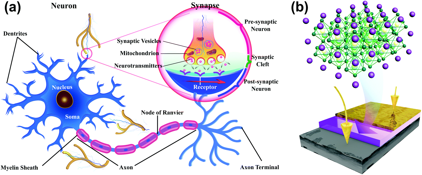 | ||
| Fig. 1 Schematics of (a) a biological neuron and (b) a two-terminal artificial synapse based on HP. | ||
The XRD patterns (Fig. 2a) of MAPbClBr2 and MAPbBr3 thin films slightly differed. MAPbBr3 crystallites show sharp diffraction peaks at 14.88°, 30.12° and 45.90°, which correspond to the (100), (200) and (300) planes, respectively. These results indicate that the MAPbBr3 crystals are quite pure in phase and preferred-oriented on growth. Doping of MAPbBr3 with Cl led to lattice distortion and crystal defects, so the intensity of diffraction peaks decreased for the MAPbClBr2 crystals and another peak that corresponds to the (210) plane appeared. To further confirm the existence of Cl, XPS was performed to study the distributions of surface component. The full scan XPS spectra (Fig. 2b) show carbon, nitrogen, lead and bromine in both specimens, and an additional Cl 2p peak appeared at 198 eV in MAPbClBr2; this peak indicates that the Cl had been incorporated into the crystal lattice.
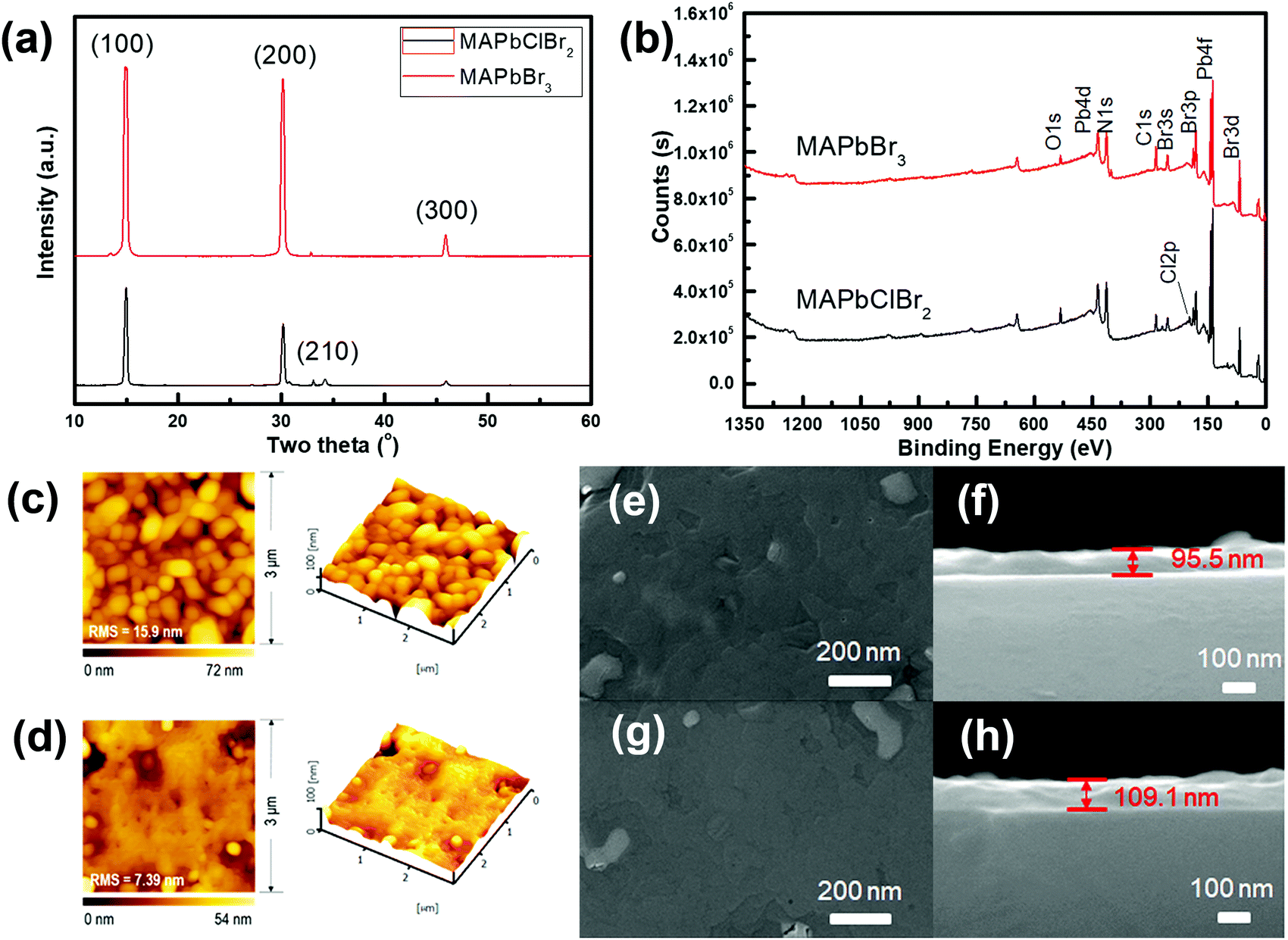 | ||
| Fig. 2 (a) XRD patterns of the MAPbClBr2 and MAPbBr3 HP films. (b) XPS full scan spectra of the MAPbClBr2 and MAPbBr3 HP films. (c) AFM images of the MAPbClBr2 thin film. (d) AFM images of the MAPbBr3 thin film. Top-view SEM images of the (e) MAPbClBr2 and (g) MAPbBr3 thin films. Cross-sectional SEM images of the (f) MAPbClBr2 and (h) MAPbBr3 thin films. | ||
The surface roughness and morphology of the MAPbClBr2 and MAPbBr3 thin films were recorded using AFM and SEM (Fig. 2c–h). Both thin films had a smooth surface with a root-mean-square (RMS) roughness of 15.9 nm for MAPbClBr2 and 7.39 nm that for MAPbBr3, and no obvious separate grains formed during the film growth. SEM cross-sectional images determined that the MAPbClBr2 films were 95.5 nm thick and the MAPbBr3 films were 109.1 nm thick.
Synaptic plasticity is the ability of synaptic connections to strengthen or weaken in response to external stimuli over time, which is the biological basis of signal transmission between neurons. Synaptic plasticity can be mainly divided into short-term plasticity (STP) and long-term plasticity (LTP).34 STP is recognized as the key element to extract valuable information efficiently while the brain is processing a huge number of stimuli.35 EPSC is caused by a temporary depolarization of the post-synaptic membrane potential, and it is one of the most common forms of STP.
To emulate this excitatory response in our artificial synapse, a synaptic device based on MAPbClBr2 was fabricated to mimic the biological synapse. The top and bottom electrodes served as the pre-synaptic and post-synaptic membranes, respectively, and the active layer of MAPbClBr2 acted as the synaptic cleft. A small constant voltage bias (0.1 V) was applied to the bottom electrode as a reading voltage, and a transient pulse with an amplitude of −0.5 V was applied to the top electrode to set up a temporary electric field across the HP thin film. The external pulse caused an increase in EPSC, which then decayed to its initial state (Fig. 3a). This phenomenon may be ascribed to the migration of halides and ion vacancies in response to the applied electrical field. When the input pulse arrived, the halide ions in HPs would migrate in an orderly fashion under the electric field force; as a result, the HP's conductivity increased substantially. Therefore, the artificial synapses showed memristive behavior, triggering a transient non-linear current that is analogous to EPSC in biological synapses. When the external stimulus was removed, the halide ions diffused back to their equilibrium positions under the effect of a concentration gradient, so the HP's electrical conductivity decreased to its initial state. The halide ion migration and the vacancy-assisted diffusion have dominant effects on the control over the multiple resistance levels of HP-based synaptic devices.
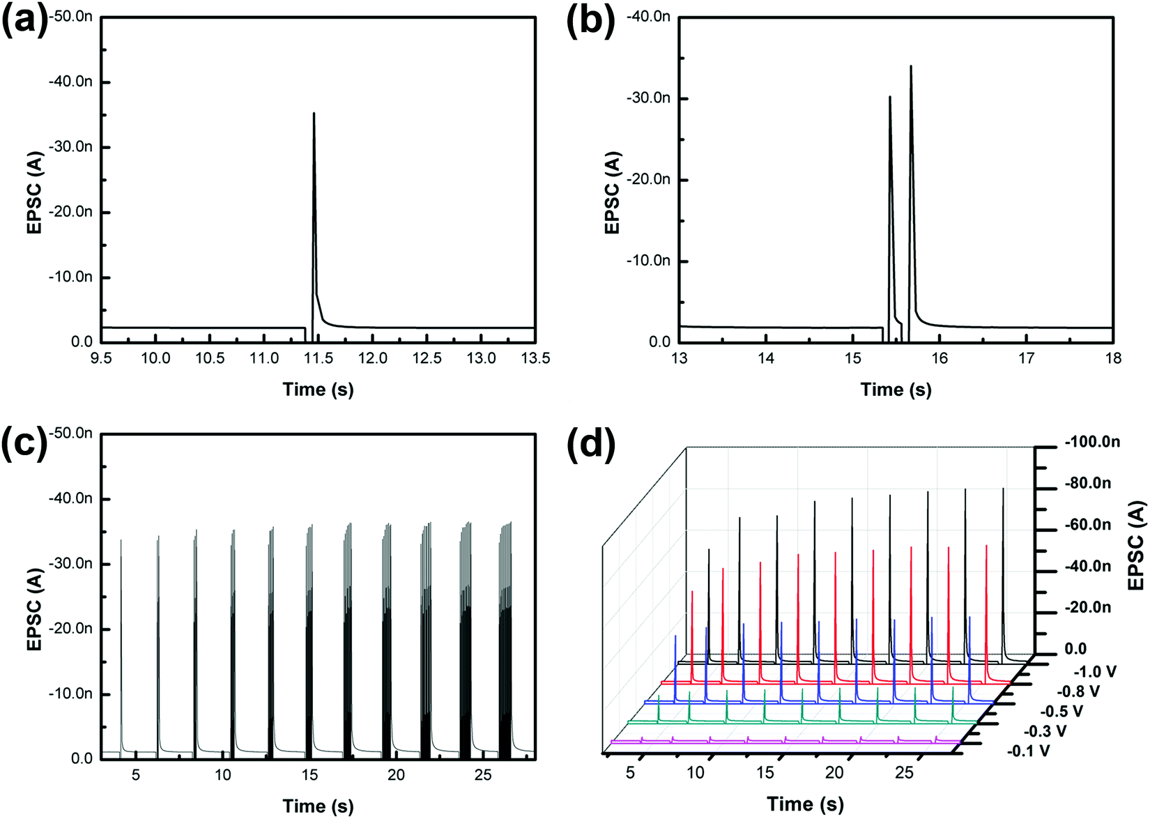 | ||
| Fig. 3 (a) EPSC triggered by a single pre-synaptic spike (−0.5 V, 25 ms duration) in a MAPbClBr2-based artificial synapse. (b) EPSC triggered by a pair of pre-synaptic spikes with an interval time of 240 ms in a MAPbClBr2-based artificial synapse. (c) SNDP from 1 to 11 spikes (−0.5 V) in a MAPbClBr2-based artificial synapse. (d) SDDP at different pulse voltages in a MAPbClBr2-based artificial synapse. | ||
During the biological synaptic transmission, the amount of Ca2+ that is delivered to the pre-synaptic membrane increases if the pre-synaptic neuron is stimulated twice in quick succession. This result is an increase in the quantity of neurotransmitters that are released. The result is PPF, by which the absolute value of the second EPSC is larger than the first. PPF is a significant form of STP that exploits the dynamic increase in the release of neurotransmitters; this increase sensitizes the synapses to external stimuli and has applications in several processes, including signal processing and sound-source localization.36
PPF was demonstrated in our artificial synapse based on MAPbClBr2 (Fig. 3b). EPSCs, triggered by a pair of consecutive input pulses, were observed. The second EPSC had 12.5% higher amplitude than the first EPSC. The migration of the halide ions in HPs caused an increase in the conductance of the synaptic device, and the ions tended to quickly return to their positions after the first external stimulus. However, the second input impulse arrived before all of the ions could diffuse back to their equilibrium sites. Therefore, both migration distance and quantities of the halide ions were increased, so the second EPSC spike was larger than the first.
Hebbian theory suggests that the repeated stimuli between two neurons can increase their synaptic transmission efficacy and enduringly improve the neural connections.37 For instance, SNDP is a learning rule, which indicates that a series of external stimuli can alter the quantity of neurotransmitters released into a synapse. To mimic SNDP in our synaptic device based on MAPbClBr2, a train of impulses with a fixed amplitude of −0.5 V and interval of 68 ms was applied to the metal top electrode as action potentials. As the number of pulses increased from one to eleven, the amplitude of EPSC spikes increased, but at a decreasing rate (Fig. 3c). The trend is a result of an increase in the number of migrated halide ions and vacancy defects in the electronic device; these increases caused an increase in the conductance of the electronic device. Initially, only a few pulses were used to trigger EPSC, so a later pulse could drive many halide ions and yield a huge increase in conductance. Nevertheless, as the number of pulses further increased, the diffusion of halide ions decreased because they were being driven into an increasing concentration gradient.
In a biological synapse, the increase in the duration or strength of a stimulus causes an increase in the quantity of chemical neurotransmitters that are released from the pre-synaptic vesicles into the synaptic cleft. Analogously, changes in the pulse width and amplitude of input signals yielded emulation of both SDDP and SVDP in the artificial synapse based on MAPbClBr2 (Fig. 3d). When the pulse duration was increased under a constant pulse amplitude, the EPSC peaks increased at first but at a decreasing rate. This phenomenon occurred because the total number of mobile halide ions was finite. During the initial stage, only a small portion of the halide ions was driven to move under an external electric field when the pulse duration was short. With the increase in the pulse duration, the number of migrated halide ions increased and the residual number of mobile halide ions decreased, so the effectiveness of an increase in the pulse duration declined. Similarly, when the pulse voltage was increased with constant pulse duration the EPSC peaks also increased.
Energy consumption was calculated as E = Ipeak × V × td, where Ipeak is the peak of EPSC, V is the pulse amplitude, and td is the pulse duration. The minimal energy consumption was estimated to be 5.8 pJ per synaptic event for the −0.1 V pulse. This energy consumption could further be reduced by decreasing the pulse duration.
An artificial synapse based on pure MAPbBr3 was fabricated using identical synthesis processes and device structures as for the artificial synapse based on MAPbClBr2. A series of consecutive pulses evoked a higher EPSC in the artificial synapses based on MAPbClBr2 (Fig. 4a) than that in artificial synapses based on MAPbBr3 (Fig. 4b). The presented EPSCs were the last EPSC peaks, which were also the largest per train of stimuli. The number and voltage of pulses both influenced the overall current amplitude. As the pulse number and voltage increased, EPSC also increased; these changes emulated SNDP and SDDP, respectively. The proportional increase decreased with an increase in the pulse number, but increased as the pulse voltage increased. The EPSCs were smaller in the artificial synapses based on MAPbBr3 than in the artificial synapses based on MAPbClBr2 under the same test conditions. The difference might have occurred because chloride ions (Cl−) have a smaller diameter than bromide ions (Br−).38 Small ions can migrate and diffuse more easily and freely than large ions can. Another reason may be that Cl− in perovskite halides have a relatively lower activation energy Ea than Br−,39–41 so Cl− can move more readily than Br− along the grain boundaries in HP thin films, resulting in a larger increase in the conductance of the HP film. However, both artificial synapses responded to a 0.1 V stimulus, which was comparable with that of a biological synapse.
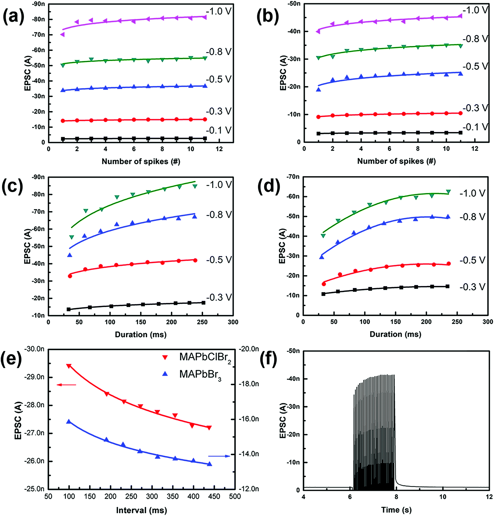 | ||
| Fig. 4 SNDP of (a) MAPbClBr2- and (b) MAPbBr3-based artificial synapses at different voltages. The SDDP statistical graphs of (c) MAPbClBr2- and (d) MAPbBr3-based artificial synapses at different voltages. (e) SRDP statistical graphs (−0.5 V). (f) EPSCs triggered by 30 consecutive pulses (−0.5 V). | ||
Both devices also showed SDDP (Fig. 4c and d). Prolonged impulse duration initially caused a significant increase in EPSC, but the proportional increase declined as the duration increased. This kind of nonlinear increase indicates that the multi-resistance states could be realized by finely adjusting the pulse number, voltage and duration.
As an extension of Hebbian learning rules, SRDP describes how the firing rate of pre-synaptic spikes affects synaptic plasticity, which is closely related to associative memory, learning and forgetting behaviors of the brain.42 Both of these HP-based synaptic devices mimicked SRDP after the application of ten consecutive impulses with different pulse intervals (Fig. 4e). The current recorded here was the EPSC triggered by the tenth input pulse. EPSCs were different in the devices, but in both devices they decreased as the pulse interval increased. When the pulse interval was small (i.e., rate was high), the back diffusion of the halide ions was inhibited by the second impulse, so the conductance increased. The suppression of the back diffusion would weaken as the pulse interval increased, so the enhancement effect became inefficient.
To investigate whether LTP could be emulated in the artificial synapses based on MAPbClBr2, 30 consecutive pulses were applied to the device. EPSC increased continuously as the pulses were being applied, but decayed to the initial state within 100 ms (Fig. 4f). Although this HP-based artificial synapse exhibits poor memory retention, this ultrasensitive characteristic provides potential applications in sensory nervetronics to mimic a peripheral nerve system.43,44
Conclusion
We fabricated the two-terminal artificial synapses from a mixed halide perovskite (MAPbClBr2) thin film, which mimicked a series of synaptic functional behaviors, such as EPSC, PPF, SNDP, SDDP, SVDP and SRDP. These synaptic characteristics occurred because the electric field drove the migration of halide ions and ion vacancies in the HP thin films. These artificial synaptic devices are ultrasensitive and energy-efficient, and can be applicable to Tri-Co neuromorphic electronics and sensory-motor nervetronics.Conflicts of interest
The authors have no conflicts of interest.Acknowledgements
This research was supported by the National 1000 Youth Talents Plan of China (BF180271), Hundred Young Academic Leaders Program of Nankai University, Natural Science Foundation of Tianjin (18JCYBJC16000), the 111 Project (B16027), the International Cooperation Base (2016D01025) and Tianjin International Joint Research and Development Center.References
- S. B. Laughlin, R. R. de Ruyter van Steveninck and J. C. Anderson, Nat. Neurosci., 1998, 1, 36–41 CrossRef CAS PubMed.
- C. C. Petersen and S. Crochet, Neuron, 2013, 78, 28–48 CrossRef CAS PubMed.
- G. Perea, M. Navarrete and A. Araque, Trends Neurosci., 2009, 32, 421–431 CrossRef CAS PubMed.
- V. M. Ho, J. A. Lee and K. C. Martin, Science, 2011, 334, 623–628 CrossRef CAS PubMed.
- D. A. Drachman, Neurology, 2005, 64, 2004–2005 CrossRef PubMed.
- D. Kuzum, R. G. Jeyasingh, B. Lee and H. S. Wong, Nano Lett., 2012, 12, 2179–2186 CrossRef CAS PubMed.
- Q. Lai, L. Zhang, Z. Li, W. F. Stickle, R. S. Williams and Y. Chen, Adv. Mater., 2010, 22, 2448–2453 CrossRef CAS PubMed.
- M. Costa-Mattioli, W. S. Sossin, E. Klann and N. Sonenberg, Neuron, 2009, 61, 10–26 CrossRef CAS.
- M. Mayford, S. A. Siegelbaum and E. R. Kandel, Cold Spring Harbor Perspect. Biol., 2012, 4, a005751 Search PubMed.
- S. J. Martin, P. D. Grimwood and R. G. Morris, Annu. Rev. Neurosci., 2000, 23, 649–711 CrossRef CAS PubMed.
- Y. H. Liu, L. Q. Zhu, P. Feng, Y. Shi and Q. Wan, Adv. Mater., 2015, 27, 5599–5604 CrossRef CAS PubMed.
- G. Indiveri, E. Chicca and R. Douglas, IEEE Trans. Neural Networks, 2006, 17, 211–221 CrossRef PubMed.
- Y. V. Pershin and M. Di Ventra, Neural Networks, 2010, 23, 881–886 CrossRef.
- D. B. Strukov, G. S. Snider, D. R. Stewart and R. S. Williams, Nature, 2008, 453, 80–83 CrossRef CAS PubMed.
- T. Chang, S.-H. Jo, K.-H. Kim, P. Sheridan, S. Gaba and W. Lu, Appl. Phys. A: Mater. Sci. Process., 2011, 102, 857–863 CrossRef CAS.
- Z. Q. Wang, H. Y. Xu, X. H. Li, H. Yu, Y. C. Liu and X. J. Zhu, Adv. Funct. Mater., 2012, 22, 2759–2765 CrossRef CAS.
- Z. H. Tan, R. Yang, K. Terabe, X. B. Yin, X. D. Zhang and X. Guo, Adv. Mater., 2016, 28, 377–384 CrossRef CAS PubMed.
- S. Saighi, C. G. Mayr, T. Serrano-Gotarredona, H. Schmidt, G. Lecerf, J. Tomas, J. Grollier, S. Boyn, A. F. Vincent, D. Querlioz, S. La Barbera, F. Alibart, D. Vuillaume, O. Bichler, C. Gamrat and B. Linares-Barranco, Front. Neurosci., 2015, 9, 51 Search PubMed.
- E. E. Josberger, Y. Deng, W. Sun, R. Kautz and M. Rolandi, Adv. Mater., 2014, 26, 4986–4990 CrossRef CAS PubMed.
- C. Diorio, P. Hasler, A. Minch and C. A. Mead, IEEE Trans. Electron Devices, 1996, 43, 1972–1980 CrossRef CAS.
- C. Wu, T. W. Kim, H. Y. Choi, D. B. Strukov and J. J. Yang, Nat. Commun., 2017, 8, 752 CrossRef PubMed.
- S. D. Stranks, G. E. Eperon, G. Grancini, C. Menelaou, M. J. Alcocer, T. Leijtens, L. M. Herz, A. Petrozza and H. J. Snaith, Science, 2013, 342, 341–344 CrossRef CAS PubMed.
- L. Dou, Y. M. Yang, J. You, Z. Hong, W. H. Chang, G. Li and Y. Yang, Nat. Commun., 2014, 5, 5404 CrossRef CAS PubMed.
- X. Hu, X. Zhang, L. Liang, J. Bao, S. Li, W. Yang and Y. Xie, Adv. Funct. Mater., 2014, 24, 7373–7380 CrossRef CAS.
- M. R. Filip, G. E. Eperon, H. J. Snaith and F. Giustino, Nat. Commun., 2014, 5, 5757 CrossRef CAS PubMed.
- A. Kojima, K. Teshima, Y. Shirai and T. Miyasaka, J. Am. Chem. Soc., 2009, 131, 6050–6051 CrossRef CAS PubMed.
- I. Yamada, H. Fujii, A. Takamatsu, H. Ikeno, K. Wada, H. Tsukasaki, S. Kawaguchi, S. Mori and S. Yagi, Adv. Mater., 2017, 29, 1603004 CrossRef PubMed.
- W. S. Yang, B. W. Park, E. H. Jung, N. J. Jeon, Y. C. Kim, D. U. Lee, S. S. Shin, J. Seo, E. K. Kim, J. H. Noh and S. I. Seok, Science, 2017, 356, 1376–1379 CrossRef CAS PubMed.
- R. Prasanna, A. Gold-Parker, T. Leijtens, B. Conings, A. Babayigit, H. G. Boyen, M. F. Toney and M. D. McGehee, J. Am. Chem. Soc., 2017, 139, 11117–11124 CrossRef CAS PubMed.
- S. Wang, Y. Jiang, E. J. Juarez-Perez, L. K. Ono and Y. Qi, Nat. Energy, 2016, 2, 16195 CrossRef.
- J. Zhang, R. Chen, Y. Wu, M. Shang, Z. Zeng, Y. Zhang, Y. Zhu and L. Han, Adv. Energy Mater., 2018, 8, 1701981 CrossRef.
- Y. Yuan and J. Huang, Acc. Chem. Res., 2016, 49, 286–293 CrossRef CAS PubMed.
- Z. Xiao, Y. Yuan, Y. Shao, Q. Wang, Q. Dong, C. Bi, P. Sharma, A. Gruverman and J. Huang, Nat. Mater., 2015, 14, 193–198 CrossRef CAS PubMed.
- W. C. Abraham and M. F. Bear, Trends Neurosci., 1996, 19, 126–130 CrossRef CAS PubMed.
- R. S. Zucker and W. G. Regehr, Annu. Rev. Physiol., 2002, 64, 355–405 CrossRef CAS PubMed.
- J. Kim and B. E. Alger, J. Neurosci., 2001, 21, 9608–9618 CrossRef CAS PubMed.
- G.-Q. Bi and M.-M. Poo, Annu. Rev. Neurosci., 2001, 24, 139–166 CrossRef CAS PubMed.
- W. Xu, T. L. Nguyen, Y.-T. Kim, C. Wolf, R. Pfattner, J. Lopez, B.-G. Chae, S.-I. Kim, M. Y. Lee, E.-Y. Shin, Y.-Y. Noh, J. H. Oh, H. Hwang, C.-G. Park, H. Y. Woo and T.-W. Lee, Nano Energy, 2018, 48, 575–581 CrossRef CAS.
- W. Xu, H. Cho, Y. H. Kim, Y. T. Kim, C. Wolf, C. G. Park and T. W. Lee, Adv. Mater., 2016, 28, 5916–5922 CrossRef CAS PubMed.
- H. C. Liao, P. J. Guo, C. P. Hsu, M. Lin, B. H. Wang, L. Zeng, W. Huang, C. M. M. Soe, W. F. Su, M. J. Bedzyk, M. R. Wasielewski, A. Facchetti, R. P. H. Chang, M. G. Kanatzidis and T. J. Marks, Adv. Energy Mater., 2017, 7, 1601660 CrossRef.
- M. Maeda, M. Hattori, A. Hotta and I. Suzuki, J. Phys. Soc. Jpn., 1997, 68, 1058–1061 Search PubMed.
- G. Rachmuth, H. Z. Shouval, M. F. Bear and C. S. Poon, Proc. Natl. Acad. Sci. U. S. A., 2011, 108, E1266–E1274 CrossRef CAS PubMed.
- Y. Lee, J. Y. Oh, W. Xu, O. Kim, T. R. Kim, J. Kang, Y. Kim, D. Son, J. B.-H. Tok, M. J. Park, Z. Bao and T.-W. Lee, Sci. Adv., 2018, 4, eaat7387 CrossRef PubMed.
- Y. Kim, A. Chortos, W. Xu, Y. Liu, J. Y. Oh, D. Son, J. Kang, A. M. Foudeh, C. Zhu, Y. Lee, S. Niu, J. Liu, R. Pfattner, Z. Bao and T.-W. Lee, Science, 2018, 360, 998–1003 CrossRef CAS PubMed.
Footnote |
| † These authors contributed equally. |
| This journal is © the Partner Organisations 2019 |