
Intrinsically stretchable conductors and interconnects for electronic applications
Quan
Zhang
a,
Jiajie
Liang
 abc,
Yi
Huang
abc,
Huiyu
Chen
d and
Rujun
Ma
*a
abc,
Yi
Huang
abc,
Huiyu
Chen
d and
Rujun
Ma
*a
aSchool of Materials Science and Engineering, National Institute for Advanced Materials, Nankai University, Tianjin 300350, P. R. China. E-mail: malab@nankai.edu.cn
bKey Laboratory of Functional Polymer Materials of Ministry of Education College of Chemistry, Nankai University, Tianjin 300350, P. R. China
cTianjin Key Laboratory of Metal and Molecule-Based Material Chemistry and Collaborative Innovation Center of Chemical Science and Engineering (Tianjin), Nankai University, Tianjin 300350, P. R. China
dSchool of Materials Science and Engineering, North University of China, Taiyuan 030051, P. R. China
First published on 10th April 2019
Abstract
Recently, stretchable electronics with excellent mechanical stretchability and electrical properties have potential important applications in various electronic devices. Intrinsically stretchable conductors and interconnects are the indispensable components of soft electronics, including mechanical sensors, wearable devices, energy harvesters and biomedical devices. In this review, we summarize the recent progress in intrinsically stretchable conductors and interconnects as well as their applications in stretchable electronics. The focus will be on a variety of intrinsically stretchable conductors and interconnects based on metallic nanowires, liquid metals, carbon nanomaterials, conducting polymers and conductive composites. Moreover, directions for further research of intrinsically stretchable conductors and interconnects will also be discussed.
 Quan Zhang | Quan Zhang received his PhD from Beijing Normal University in China. Currently, he is a postdoctoral researcher at Nankai University. His PhD work focuses on the influence of interface effects on electron transportation in carbon nanotubes and carbon nanotube-based composites. |
 Jiajie Liang | Jiajie Liang received his PhD from the Institute of Polymer Chemistry of Nankai University, China. He is currently a professor at the School of Materials Science and Engineering, Nankai University. His research is focused on new functional materials to enable innovative applications on various kinds of stretchable electronics. |
 Yi Huang | Yi Huang received his PhD in Materialogy from Sichuan University, China. Currently, he is a professor at the School of Materials Science and Engineering, Nankai University. His work focuses on controlled synthesis and application of carbon nanomaterials, functional polymer materials, and nano-composites and -devices. |
 Huiyu Chen | Huiyu Chen received his PhD in Advanced Materials and Engineering from Sungkyunkwan University, South Korea. He is currently an associate professor at the School of Materials Science and Engineering, North University of China. His research interests focus on inorganic nanomaterials, functional composites and energy materials. |
 Rujun Ma | Rujun Ma received his PhD from the Department of Nanoscience and Nanotechnology at Sungkyunkwan University, South Korea. He is currently a professor at the School of Materials Science and Engineering, Nankai University, China. He mainly works on flexible electrocaloric cooling devices and stretchable electronics. |
1. Introduction
The rise of stretchable conductive materials has expanded the well-known traditional electronic circuits into new application areas recently, such as stretchable electrodes,1–3 stretchable displays,4–6 soft robots,7–14 stretchable sensors,15–21 electronic skin22–26 and stretchable transistors.27–29 Stretchability is a crucial property for stretchable electronics since earlier research focused on the mechanical compliance of human motion. Meanwhile, they must be conductive under large strains and recover their initial properties after removing the induced load.30 Thus, the ability to withstand mechanical load represents outstanding robustness, compared with traditional electronic circuits.As stretchable conductors are the alternatives of traditional conductors, their performance should meet the actual demands in corresponding applications. Taking stretchable electrodes and mechanical sensors as examples, the requirement for stretchable electrodes is a small change in resistance under large tensile strain, whereas a large change in resistance under small tensile strain is necessary for mechanical sensors. It means that the selection of stretchable conductors should be based on the practical applications. Besides stretchable and conductive properties, these materials have other characteristics, such as the selection of various components and structures which enable self-healing, light-weight, biocompatibility, anti-oxidative properties, transparency, and so on. These additional performances enrich the applications for soft electronics and overcome the defects of traditional devices. Fig. 1 shows the classifications, physical and chemical properties, and applications (Coconut trees) in stretchable electronics of intrinsically stretchable conductors and interconnects (Soil).
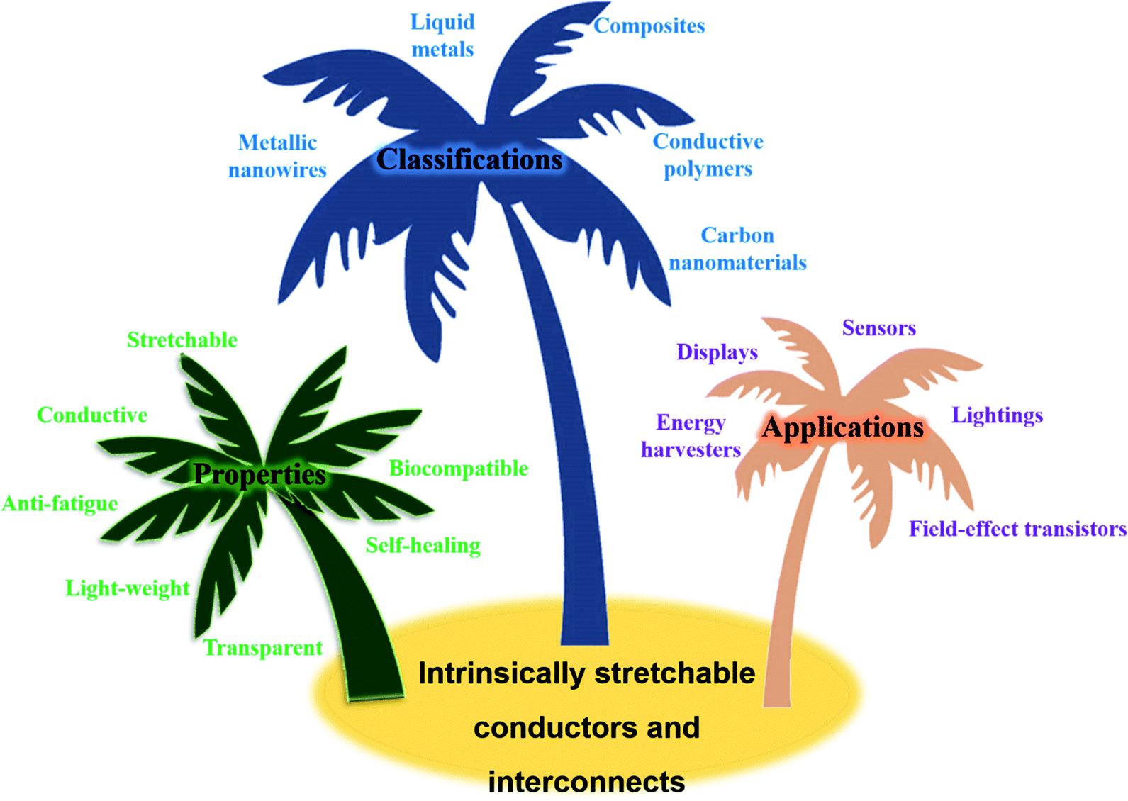 | ||
| Fig. 1 Classification, physical and chemical properties, and applications in stretchable electronics of intrinsically stretchable conductors and interconnects. | ||
Generally, to enable mechanical stretchability of electronic materials, two different strategies can be found in the literature. The first approach is shape engineering of non-stretchable conductive materials into wavy or meandering structures to eliminate the tensile strain in these non-stretchable materials when a tensile force is applied.2,5,17,31–44 The second one is fulfillment of intrinsically stretchable conductive materials with large mechanical stretchability and simple fabrication processes.45–48 Wavy or meandering structures, which are based on architectural consideration, can form stretchable electrodes with reversible elasticity by utilizing traditional non-stretchable conductive materials. Consequently, the stretchability of the developed electrode can be realized up to a pre-stretched value where the active electrodes are not stretched. Moreover, the good performance of electrodes can be preserved with the mechanical properties of the elastomer. However, the electrode density and stretchability exhibited a trade-off relationship for wavy or meandering structures. Meanwhile, engineering of stretchable architectures still has many challenges and obstacles. In addition, the predefined directions of conductive materials restrict the elasticity of engineered shape and the cost of fabrication is not low. To overcome these limitations, intrinsically stretchable conductive materials as a viable approach entailing the elastomeric stretchability for each component have been investigated.46,49–51 Intrinsically stretchable conductive materials do not rely on a two-dimensional (2D) spring structure to absorb tensile load compared with patterned or pre-strained conductive materials. The electron transportation paths still meet the conductivity requirements under a tensile strain, although there is an obvious micro-structural deformation. Intrinsically stretchable electronic devices can simplify the manufacturing process for achieving miniaturization, integrate the device with high density, eliminate the need for higher order microstructures, tolerate large strain and have low cost compared with geometrically arranged stretchable electronic devices.50,52 In Table 1, we summarize a few representative intrinsically stretchable conductors. Besides stretchability and conductivity, other unique characteristics enriched the functions of stretchable devices prepared by intrinsically stretchable conductive materials.
| Classifications | Design principles | Materials | Stretchability (%) | Initial conductivity | Other characteristics | Applications |
|---|---|---|---|---|---|---|
| Metals | Metallic NW network on polymer | Au nanotrough54 | 50 | ∼2.2 × 10⁵ S m−1 | — | — |
| AgNW network/GO69 | 100 | 20 Ω sq−1 | — | Light-emitting diode | ||
| CuNW network58 | 250 | 20 Ω sq−1 | — | Transparent conductor | ||
| AgNW network59 | 100 | 37 Ω sq−1 | — | Transparent conductor | ||
| PMN-PT/CNTs/PDMS/AgNWs71 | 250 | 4 Ω sq−1 | — | Energy harvester | ||
| Metallic NW network embedded in polymer | AgNWs/PUA4 | 120 | 10 Ω sq−1 | Transparent | Light-emitting devices and displays | |
| AgNWs/PUA72 | 50 | 15 Ω sq−1 | Transparent | Transparent thin-film transistors | ||
| Ag@Au/SBS73 | 840 | 72![[thin space (1/6-em)]](https://www.rsc.org/images/entities/char_2009.gif) 600 S cm−1 600 S cm−1 |
Biocompatible | Wearable and implantable bioelectronics | ||
| AgNWs/OTMS24 | 100 | 285.23 S cm−1 | Self-healing | Electronic skin | ||
| Liquid metals | EGaIn75 | 60 | 1.865 Ω | — | Monolithically integrated stretchable circuits | |
| EGaIn81 | 250 | 3 × 10⁻⁷ Ω m−1 | — | Comb capacitor | ||
| EGaIn86 | 700 | 724 S cm−1 | Self-healing | Comb capacitor | ||
| Carbon nanomaterials | Graphene sheet on polymer | Graphene95 | 30 | ∼280 Ω sq−1 | — | — |
| Graphene nanoscolls96 | 120 | ∼1000 Ω sq−1 | Electrodes | |||
| Graphene97 | 20 | — | — | Transistors | ||
| Graphene98 | 1 | 24 Ω cm−1 | — | Sensors | ||
| Graphene99 | — | — | — | Energy harvester | ||
| Graphene framework embedded in polymer | Au–Ni@graphene/PU100 | 30 | 2.5 Ω | — | Electrodes | |
| Graphene framework/PDMS101 | 70 | 0.47 kΩ | — | Sensor | ||
| Graphene-rubber composite52 | 1000 | 0.1 S m−1 | High-rate | Bodily motion sensors | ||
| CNT yarn | CNT yarn104 | 10 | 30–46 Ω | — | Sensors | |
| CNT network on polymer | CNT paper (90 μm thickness)105 | 50 | ∼5 Ω | — | Sensors | |
| CNT network/graphene19 | 10 | — | — | Sensors | ||
| Carbon nanocoils/PDMS106 | 260 | 33.3 kΩ | — | Strain sensor | ||
| CNTs embedded in polymer | MWCNT/PEDOT:PSS107 | 50 | 0.7 kΩ cm | — | Energy harvesting and strain sensing | |
| CNTs/OTMS24 | 100 | — | Self-healing | Electronic skin | ||
| Conducting polymers | Modified conducting polymers | Polyacrylamide and PPy114 | 800 | 1–2 kΩ m | Low Young's modulus, transparent | Transparent and flexible strain sensors |
| F-hydrogel115 | 500 | — | Self-healing | Wearable soft strain sensors | ||
| DN hydrogel | DN hydrogel30 | 350 | 3.04 S m−1 | Self-healing | Strain sensors | |
| DN hydrogel110 | 3200 | ∼0.02 S cm−1 | Self-healing | Wearable sensors | ||
| DN hydrogel111 | 300 | 36.8 ± 4.1 mS m−1 | Self-healing | Wearable sensors | ||
| DN hydrogel112 | 975 | 3.4 S m−1 (1 MHz) | Self-healing | Wearable sensors | ||
| DN hydrogel116 | 1000 | 55 kΩ | Self-healing, 3D printing | Strain sensor | ||
| Conductive composites | Polymer filled with metallic NPs | Ag nanoflowers/PU3 | 776 | 41245 S cm−1 |
— | Electrodes |
| Ag NPs-decorated MWCNTs/Ag flakes/PDMS118 | 30 | 3100 S cm−1 | — | Electrodes | ||
| Ag flakes/Ag NPs/Fluorine rubber128 | 300 | 6168 S cm−1 | — | Electrodes | ||
| Au NPs/PU120 | 115 | 11000 S cm−1 |
— | Electrodes | ||
| Au NPs/PU120 | 486 | 1800 S cm−1 | — | Electrodes | ||
| Polymer filled with carbon nanomaterials | MWCNTs/HEPCP23 | 340 | — | Near-IR and temperature sensitivity | Electronic skin | |
| CNTs/PVA/borax129 | 1000 | ∼105 Ω | Self-healing | Human-motion detection | ||
| CBs/PDMS122 | ∼280 | — | Strong adhesion in dry and wet environment | Electronic skin | ||
| Graphene/putty16 | 100 | 4 MΩ | Viscoelastic | Electromechanical sensor | ||
| PPy/CBs/PDMS127 | 150 | 0.3 Ω m | Waterproof and self-charging power | Energy harvester | ||
This review focuses on the recent progress in intrinsically stretchable conductors and interconnects for applications in stretchable electronics. In the next five sections, we will introduce different kinds of intrinsically stretchable conductive materials and their applications. In the last section, a conclusion about the current research status of stretchable conductors and interconnects is discussed.
2. Metallic nanowires
2.1. Metallic nanowire network on a stretchable substrate
Gold (Au) is a typical metal material with excellent conductivity and stretchability. In the 1960s, D. W. Pashley prepared a self-standing and single-crystal Au film with a thickness of about 20 nm. Experimental results showed the fracture of the self-standing Au film under a tensile strain of only 1–2%.53 The researchers also tried to evaporate an Au film with a thickness of about 80 nm on a relaxed polydimethylsiloxane (PDMS) substrate. Although the Au film was able to endure up to 20% strain, it exhibited a dramatic increase in resistance.54,55 The aforementioned facts implied that the metal film could not satisfy the requirements of an intrinsically stretchable conductor.The rise of one-dimensional (1D) metal nanostructures (such as nanowires (NWs) and nanotroughs) makes it possible to directly apply metals in intrinsically stretchable electrodes.54 Compared with classical metal films, the conductive percolation network formed by metal NWs has both excellent conductivity and stretchability. The conductive and stretchable properties of the percolation network strongly depend on the effective contact between NWs. A series of works, such as heat welding,48,56 plasma welding,57,58 capillary-induced cold welding,59 mechanical pressing,60 and electrochemical coating,61–63 have been developed to improve the point contact at NW–NW junctions. Normally, the metal-NW percolation network is used as a transparent electrode. When the NW percolation network is coated on a transparent elastomer, a transparent conductive stretchable layer is formed. Such a stretchable and conductive layer is a critical component that determines whether current flows smoothly and signals are transferred effectively in stretchable devices.
Silver nanowire (AgNW) networks can exhibit desirable optical, mechanical and electrical properties and can be fabricated via high-speed, low-cost and large-scale roll-to-roll processes on various types of substrates.57,64–67 Due to their large electrical conductivity, mechanical flexibility and high transparency, AgNWs as an alternative material are highly expected to replace indium tin oxide (ITO) for next generation electronic devices.68 The sheet resistance and mechanical strength of the network are determined by the contacts between NWs. Liang et al. enhanced the mechanical strength of AgNW networks by deposition of graphene oxide (GO) sheets.69 The experimental results showed that the sheet resistance of AgNW networks reduced 50 times after soldering GO sheets. Simultaneously, the transmittance of the electrodes remained about 90% in the visible and near infrared region. Under a tensile strain of 100%, the increase in resistance of the network coating on polyurethane acrylate (PUA) is less than 20-fold. After repeated 40% stretching and releasing, the resistance of the electrode at the releasing state increased 4 times compared with its initial value. Fig. 2a shows a polymer light-emitting diode (PLED) with a AgNW network operated in a steady state under different tensile strains.
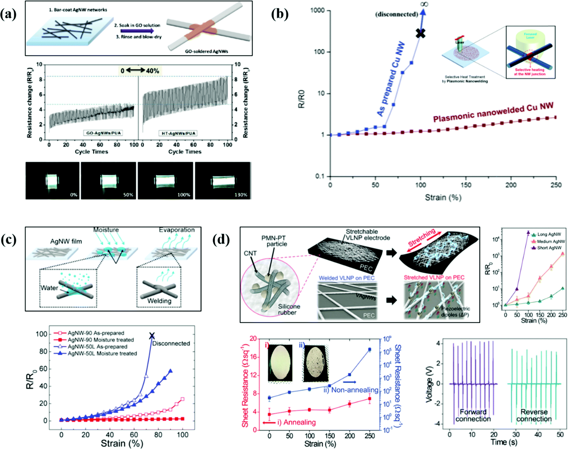 | ||
| Fig. 2 Stretchable electrodes fabricated by coating a metallic NW network on a stretchable substrate. (a) Schematic of the process of a GO-soldered AgNW network (up), normalized resistance of GO-AgNW/PUA and HT-AgNW/PUA electrodes with repeated 40% stretching and releasing (middle) and optical images of a PLED under different tensile strains (down). Adapted and modified with permission from ref. 69. Copyright 2014, American Chemical Society. (b) Normalized resistance of a Cu NW network under different tensile strains from 0 to 100%. The inset is the schematic of the process of plasmonic laser nanowelding. Adapted and modified with permission from ref. 58. Copyright 2014, American Chemical Society. (c) Schematic of the process of capillary–force-induced cold welding of AgNWs (up) and normalized resistance of as-prepared and moisture-treated AgNW-90 and AgNW-50L films under different tensile strains from 0 to 250% (down). Adapted and modified with permission from ref. 59. Copyright 2017, American Chemical Society. (d) Schematic of the hyper-stretchable and deformable nanocomposite generator and relative resistance change of NW percolation network electrodes with different lengths under different tensile strains (up). Change in sheet resistance of electrodes with and without annealing treatment under different tensile strains and the generated output open-circuit voltage from the device during the periodical stretching/releasing deformations (down). Adapted and modified with permission from ref. 71. Copyright 2015, Wiley-VCH. | ||
Welding is an effective method to enhance the mechanical strength and conductivity of the NW junctions. Huang et al. improved the contact properties of metallic NW junctions with the assistance of localized reactions induced by an electrical current.70 Due to the high contact resistance of the NW junctions, Joule heating was generated at a high current density and further resulted in integration of NWs. Han et al. fabricated a copper (Cu) NW network by an ultrafast plasmonic nanowelding process under ambient conditions,58 and this method was able to minimize Cu oxidation. In the visible region, the transmittance of an Ecoflex film coated with the treated NW network was larger than 80% and the sheet resistance of the film was around 100 Ω sq−1. Compared with the as-prepared conductor, the resistance of the plasmonically nanowelded Cu NW network was 4 times less than its initial value under a strain of 250%. After a cyclic test of repeated 250% stretching and releasing, the resistance at the releasing state increased by only 10%. A touchscreen panel composed of the CuNW network confirmed the applicability of the transparent electrode in practical devices (Fig. 2b).
To improve the contact of junctions, the Ren group applied capillary force as the driving force for cold welding of AgNWs.59 Different from the existing methods, a chemical reagent or specific equipment was not needed. At the nanoscale, capillary force can generate high pressure and result in the cold wedding of metallic NWs. The moisture-treated NW network had a remarkable increase in electrical conductivity and mechanical stretchability, but a negligible change in optical transmittance was observed in the visible region (Fig. 2c). The results also showed that it was possible to repair damaged NW electrodes using simple water vapor on the network. This method provided a new way to make stretchable transparent electrodes with high-performance by use of metallic NWs.
Jeong et al. designed a hyper-stretchable elastic composite generator (SEG) using a rubber-based piezoelectric elastic composite (PEC) and ultralong AgNW percolation (VLNP) electrodes. The PEC was prepared by embedding (1 − x){Pb(Mg1/3Nb2/3)O3}–x{PbTiO3} (lead magnesio niobate-lead titanate) (PMN-PT) and multi-walled carbon nanotubes (MWCNTs) into a silicone elastomer matrix. Compared with short and medium AgNW electrodes, the electrodes fabricated by long AgNWs exhibited highly stable electrical and mechanical properties under the same tensile strain. Meanwhile, an annealing treatment distinctly improved the electrical properties of AgNW electrodes by forming well-fused junctions. When the device was stretched from 0% to 200%, a transient voltage of about 4 V was generated with an electric current of 500 nA. The generated output was introduced by piezoelectricity, which depended on the composition of the PEC, the presence of CNTs, and the degree of stretching strain. They also demonstrated the possibility of applying the SEG in wearable devices to generate electrical energy from motions in daily life (Fig. 2d).71
2.2. Metallic nanowire framework embedded into a polymer
Researchers have also designed stretchable conductors with the structure of a metallic NW network embedded into a polymer matrix. Liang et al. prepared a transparent and stretchable electrode by embedding a AgNW network into PUA, and the sheet resistance was less than 1000 Ω sq−1 at 100% tensile strain.4 Then, the electrode was integrated into an elastomeric polymer light-emitting cell (PLEC). Under a uniaxial tensile strain of 120%, the light-emitting performance of the PLEC remained stable (Fig. 3a). They also fabricated a high-performance, transparent and stretchable thin-film transistor (TFT) based on AgNW-PUA. The current of the TFT at on and off states was almost unchanged under a tensile strain of 50% along the length or width direction. Fig. 3b shows the luminance of an organic light-emitting diode (OLED) driven by the stretchable TFT. When the TFT was stretched up to 30% strain, the luminance of the OLED was ∼63 cd m−2 at a gate voltage of −8.0 V.72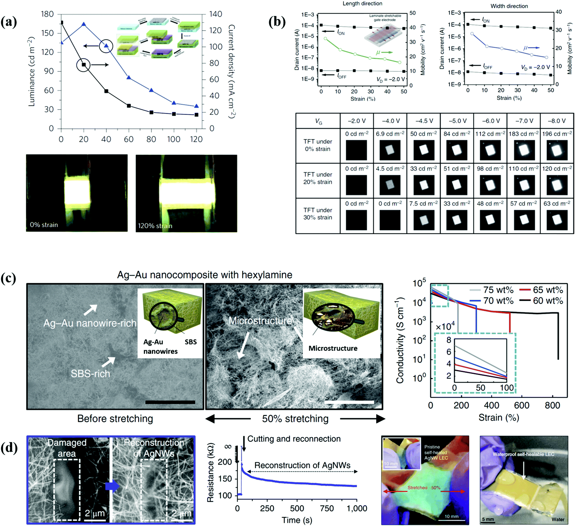 | ||
| Fig. 3 Stretchable electrodes fabricated by embedding a metallic NW framework into a polymer. (a) Current density and luminance characteristics of a PLEC device at 12 V under different strains from 0% to 120% (up) and optical images of a PLEC biased at 14 V under tensile strains from 0% to 120% (down). The inset is the schematic of the preparation process of an elastic transparent AgNW-PUA electrode and a stretchable PLEC device based on the AgNW-PUA electrode. Adapted and modified with permission from ref. 4. Copyright 2013, Nature Publishing Group. (b) ION, IOFF and mobility of a TFT as a function of applied strain along the channel length and width direction (up). The inset is the schematic of a stretchable TFT. Luminance of an OLED driven by the stretched TFT under different inputs (down). Adapted and modified with permission from ref. 72. Copyright 2015, Nature Publishing Group. (c) SEM images of Ag–Au NW composites before and after stretching (left) and conductivity change of the nanocomposites with different weight fractions of NWs under different tensile strains (right). The insets are microstructural schematics of the Ag–Au NW composite. Adapted and modified with permission from ref. 73. Copyright 2018, Nature Publishing Group. (d) SEM images of the AgNW network before and after self-healing (left) and real-time electrical monitoring of the reconstruction of the AgNW network (middle). A light emitting capacitor showing reliable stretchability and waterproofness (right). Adapted and modified with permission from ref. 24. Copyright 2018, Nature Publishing Group. | ||
Choi et al. prepared highly conductive biocompatible and stretchable composites based on Ag–Au NWs and styrene butadiene styrene (SBS) polymer.73 An Au layer coating on the ultralong AgNWs effectively prevented Ag oxidation and ion leaching, conducive to improving biocompatibility. Due to the effect of phase separation during the solvent drying, extensive Ag–Au NW-rich regions and SBS-rich regions formed in the composite. After hot rolling-press treatment, the maximum stretching strain of the composite increased from 260% to 840%. A skin-like mesh device as an implantable cardiac mesh based on Ag–Au composites was fabricated. There was a distinctly abnormal electrical signal from the diseased compared with the healthy heart. The analysis accuracy was comparable to that of a common electrocardiogram (Fig. 3c).
The Bao group demonstrated a self-healable conductive 1D nanostructured network of composites which were fabricated by embedding an elastic conductive network (AgNWs and CNTs) into PDMS–MPU0.4–IU0.6.24 Electrical and mechanical properties of the composites were recovered using a dynamic supramolecular crosslinked polymer network at the contact interface. The materials still had high robustness even after repeating the damage–healing process. A series of fully integrated electronic/optoelectronic multi-functional self-healable electronic systems were fabricated, such as self-healable and stretchable sensors, electroluminescent skin, and integrated electronic skin with autonomous self-healing ability (Fig. 3d).
3. Liquid metals
Liquid metals have both metallic and fluidic properties at or near room temperature. Among standard metals, mercury (Hg) is the only liquid metal and gallium (Ga), rubidium (Rb) and Cesium (Cs) belong to low-melting metals. Ga-based alloys, which have lower vapor pressure at room temperature and lower toxicity than those of Hg, are attractive in intrinsically stretchable conductors. Due to the fluidic properties, liquid metals must be fully encapsulated into elastomers when they are used in electronic devices. In this way, the elastomers maintain their intrinsic softness, which determines the stretchability of the composite electrodes.The methods to pattern liquid metals can be divided into four categories, namely, lithography-enabled,74,75 injection,76–79 additive80–83 and subtractive (Fig. 4a–d).84,85 Zhu et al. fabricated a core–shell fiber by injecting eutectic gallium indium (EGaIn) into poly[styrene-b-(ethylene-co-butylene)-b-styrene] (SEBS) hollow fibers. The dimension of the fibers depended on the spinning rate of collecting rollers, which influenced the maximum stretchable strain and the metallic electrical continuity (Fig. 4e). Park et al. prepared liquid metal interconnects by conventional photo-lithography and lift-off processes. The resistance of the interconnects increased by 40% under a tensile strain of 60%. Moreover, a thin film transistor (TFT) based on liquid metal interconnects was fabricated. The electrical characteristics of the TFT remained almost unchanged under different tensile strains from 0 to 50% (Fig. 4f).75 Tabatabai et al. produced a comb capacitor by depositing liquid-phase GaIn electronics on elastomers with microcontact printing. The electrical responses of the comb capacitor were consistent with theoretical predictions, by parallel or perpendicular stretching (Fig. 4g).81 The researchers also fabricated a multifunctional conductor with high fatigue resistance and self-healing ability. The experimental results showed that the mechanical and electrical properties of the Ni flakes-EGaInPs-CPU (NEC) structure were recovered simultaneously by the hydrogen bonding of the polymer matrix and fillers of the liquid metal. Even after breaking/healing, there was no performance degradation under a tensile strain of 200%, and the capacity was still unchanged after 600 charging/discharging cycles and 1000 stretching/releasing cycles (Fig. 4h).86
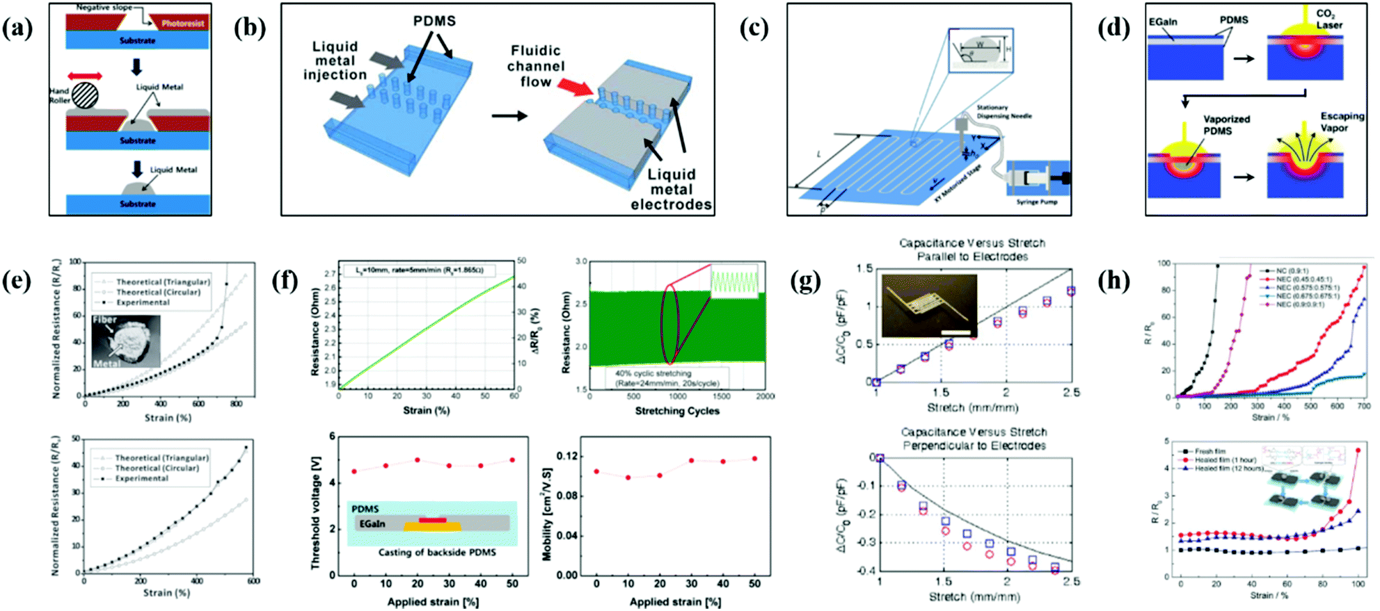 | ||
| Fig. 4 Different stretchable electrodes based on liquid metals. (a) Schematic of the patterning procedure of liquid metals. Adapted and modified with permission from ref. 75. Copyright 2016, American Chemical Society. (b) Schematic of the preparation procedure to fabricate liquid metal microelectrodes. Adapted and modified with permission from ref. 76. Copyright 2014, The Royal Society of Chemistry. (c) Schematic of a direct writing system writing a serpentine pattern. Adapted and modified with permission from ref. 82. Copyright 2014, Wiley-VCH. (d) Schematic of the preparation procedure of liquid GaIn alloys on a PDMS substrate. Adapted and modified with permission from ref. 84. Copyright 2014, Wiley-VCH. (e) The experimental and theoretical resistance of conductive fibers with two different spinning rates of 100 m min−1 (up) and 1000 m min−1 (down). The inset is the shiny core of the cross-section of the fiber. Adapted and modified with permission from ref. 79. Copyright 2013, Wiley-VCH. (f) The change in resistance of the liquid metal interconnect with tensile strain and fatigue test (up). Threshold voltage and mobility of a TFT with tensile strain (down). The inset is the schematic of a TFT on a stiff polyimide island and liquid metal interconnects. Adapted and modified with permission from ref. 75. Copyright 2016, American Chemical Society. (g) Change ratio of the capacitance of the comb capacitor as a function of stretch, parallel (up) and perpendicular (down) to electrodes. The inset is the optical image of the liquid metal pattern. Adapted and modified with permission from ref. 81. Copyright 2013, American Chemical Society. (h) Change in resistance of the NEC conductor versus tensile strain (up). Comparison of change in resistance of the NEC conductor before and after breaking/healing (down). The inset is the schematic of the mechanism for stretchable and self-healing properties of the NEC conductor. Adapted and modified with permission from ref. 86. Copyright 2018, Wiley-VCH. | ||
4. Carbon materials
4.1. Graphene-based stretchable conductors
The best-known natural allotropes of carbon are graphite, diamond and amorphous carbon. Most of the carbon materials with a graphitized structure are able to conduct electricity due to the delocalized π bonding formed by a large number of free electrons within the carbon layers. Among them, carbon nanotubes (CNTs) and graphene are typical carbon nanomaterials with excellent mechanical and electrical properties.87–93 However, the application of their outstanding properties in the macroscopic world is still a big challenge.Previous reports show that graphene exhibits a carrier mobility larger than 200000 cm2 (V s)−1 and a Young's Modulus of 1 TPa.89,94 Large-scale graphene, particularly monocrystalline graphene, is a promising candidate as a flexible electrode for application in stretchable electronic devices. Fig. 5a presents the change in resistance of graphene films transferred to pre-strained and unstrained PDMS substrates under parallel or perpendicular stretching. The resistance of the graphene film on the unstrained PDMS substrate increased by one to two times under a 6% tensile strain before mechanical fracture.95 Liu et al. analyzed the influence of the layer number of graphene on the stretchability and conductivity of the films. For 3-layer graphene, the resistance increased by about 55 times under a tensile strain of 90%.96 The experimental results showed that the change in conductivity of large-scale graphene was often dramatic under tensile strain (Fig. 5b). In addition, they designed a multi-layer structure, in which the graphene nanoscrolls were embedded into stacked graphene layers. The experimental results showed that the optimized transparent electrode was able to maintain high conductivity under large strain (Fig. 5b).96
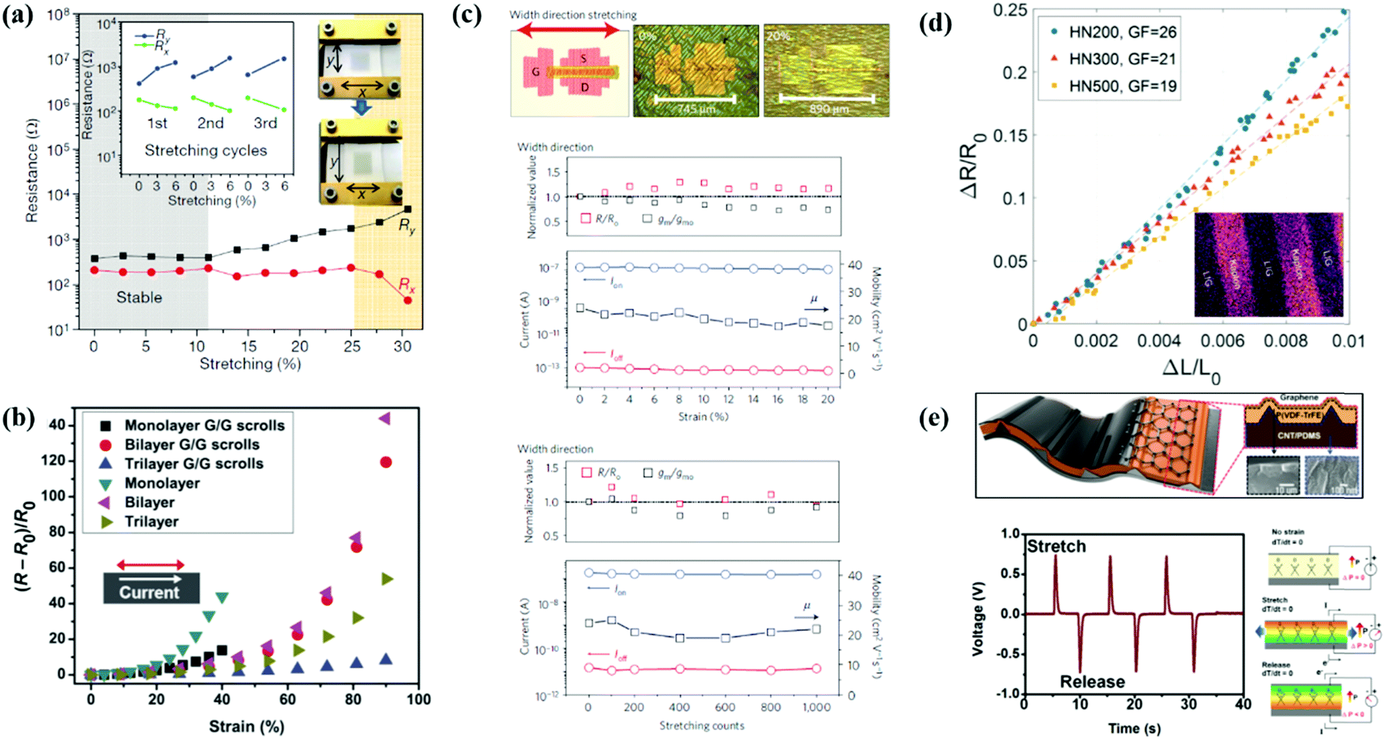 | ||
| Fig. 5 Applications of graphene films in stretchable electrodes and mechanical sensors. (a) Change in resistance of a graphene film transferred on a pre-strained and unstrained (left inset) PDMS substrate. The right inset is a comparison of the graphene film under a tensile strain. Adapted and modified with permission from ref. 95. Copyright 2009, Nature Publishing Group. (b) Normalized change in resistance of the graphene film with different layers as a function of tensile strain. Adapted and modified with permission from ref. 96. Copyright 2017, American Association for the Advancement of Science. (c) Schematic diagram and optical images of the transistors stretched perpendicular to the channel. Normalized on/off ratio, transconductance, currents (on-current (blue circle), off-current (red circle)) and mobility (black square) at different strains. Normalized on/off ratio, transconductance, currents (on-current (blue circle), off-current (red circle)), and mobility (black square) with repeated 10% stretching and releasing. Adapted and modified with permission from ref. 97. Copyright 2013, Nature Publishing Group. (d) Tensile strain measurements of devices patterned in substrates with different thicknesses. The inset is an XPS mapping of the charged C 1s peak. Adapted and modified with permission from ref. 98. Copyright 2018, Wiley-VCH. (e) Schematic of the stretchable nanogenerator (up) and piezoelectric output voltage from the devices under repeated stretching–releasing cycles (down). The insets are the schematic of the couple mechanism of the power output and piezoelectricity. Adapted and modified with permission from ref. 99. Copyright 2014, Wiley-VCH. | ||
Researchers also made use of carbon nanomaterials to prepare all-carbon thin-film transistors. In Chae's work, the electrodes, the channel, the dielectric gate, and the substrate were prepared with a graphene/CNT hybrid, CNT film, wrinkled aluminium oxide (Al2O3) film, and polyimide (PI)/PDMS film, respectively. As shown in Fig. 5c, the devices exhibited outstanding electrical properties, including an excellent on/off ratio of ∼105, a high mobility of ∼40 cm2 (V s)−1, and a low operating voltage of <1 V. It was worth stressing that the characteristics of the devices were almost unchanged under a perpendicular or parallel tensile strain of 20%. Meanwhile, no significant electrical performance degradation emerged after repeated stretching and releasing for over 1000 times.97 Recently, Carvalho et al. prepared a graphene film on a PI film by ultraviolet laser irradiation, which was sensitive to various strains.98 It also provided a low-cost and effective method for patterning of flexible and stretchable electronic devices (Fig. 5d).
Lee et al. developed a fully stretchable and flexible hybrid energy harvesting nanogenerator based on a piezoelectric polymer poly(vinylidene fluoride-trifluoroethylene) (P(VDF-TrFE)) thin film, PDMS–CNT composite and graphene.99 As shown in Fig. 5e, multilayer graphene and PDMS–CNT composite served as the top and bottom electrodes, respectively. Due to the polarization caused by stretching deformation, the device enabled generation of a pulsing output voltage under repeated stretching–releasing cycles. The output voltage increased when the tensile strain increased from 10 to 30% at a constant strain rate of 10 mm s−1. The generator also outputted the voltage under compressing deformation and thermal gradients.
Han et al. prepared Au–Ni@graphene coated polyurethane sponge (GPUS) by the electroless plating technique.100 This interconnecting structure as the skeleton led to high conductivity, good stretchability and durability of the composite. The change ratio of resistance remains stable under a tensile strain of 10% and slightly increases under a strain of 30% after 1000 stretching–releasing cycles (Fig. 6a). Jeong et al. fabricated a highly stretchable and sensitive strain sensor using a composite of fragmentized graphene foam (FGF) and PDMS.101 The FGF with a 3D structure was conductive owing to the formation of a 3D percolation network in the PDMS matrix. The sensitivity of the sensor was improved due to the large contact area between adjacent FGFs. The sensor possessed high stretchability over 70% tensile strain and fatigue resistance after 10000 stretching cycles. When the sensor was attached on the body, it could effectively detect various biosignals, which demonstrated great potential applications in wearable devices (Fig. 6b). Boland et al. prepared a conductive composite by filling graphene flakes into a rubber matrix, which was sensitive to high strains and strain rates.52 The percolation threshold of such a composite was less than 0.1%. It exhibited an initial electrical conductivity of 0.1 S m−1 and reached a tensile strain as large as 1000% (Fig. 6c). This demonstrated that the composite could be applied in medical devices for monitoring various bodily actions.
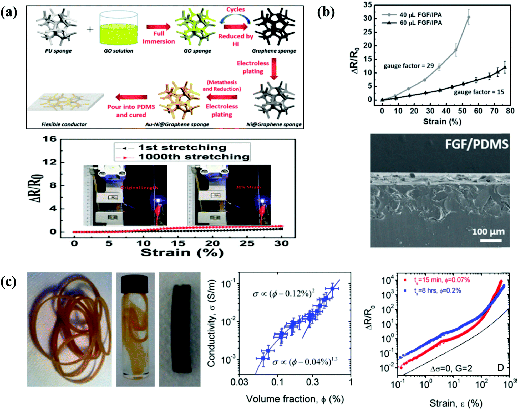 | ||
| Fig. 6 Applications of a graphene-based framework in stretchable electronic devices. (a) Schematic of the fabrication process of the Au–Ni@graphene conductor (up) and relative change in resistance of the conductor during the 1st and 1000th stretching process (down). The insets are optical images of the LED lights with the conductors at the releasing state and stretching state of 30% strain. Adapted and modified with permission from ref. 100. Copyright 2018, The Royal Society of Chemistry. (b) Change ratio of resistance of the graphene/PDMS sensor as a function of tensile strain (up) and the SEM image of the cross-section of the strain sensor (down). Adapted and modified with permission from ref. 101. Copyright 2015, Wiley-VCH. (c) Optical image of a graphene-based band (left), conductivity of graphene-based bands as a function of volume fraction of graphene flakes (middle) and relative change ratio of bands under different tensile strains (right). Adapted and modified with permission from ref. 52. Copyright 2014, American Chemical Society. | ||
4.2. Carbon nanotube-based stretchable conductors
An individual CNT is not suitable for direct application in macroscopic devices. However, by assembling carbon nanomaterials into a macroscopic structure it is possible to effectively meet the requirements in practice. It is a thermodynamic process in which the molecular interactions are a main factor to keep the stability of the structure.102 Feng et al. prepared a super-aligned CNT film by spinning from a vertical CNT array.103 In that work, the sheet resistance of the free-standing film increased from 1 kΩ sq−1 to about 2.3 kΩ sq−1 under a tensile strain of 120% perpendicular to the drawing direction.Obaid et al. investigated the electro-mechanical behavior of CNT yarns under tensile loading.104 When the tensile strain was lower than 1.6%, the resistance of the yarns could recover after removing the loading. However, the change in resistance under a stretching strain larger than 1.6% was non-recoverable. Structural analysis demonstrated that such behavior stemmed from the partial failure and sliding due to the weak van der Waals interactions between CNTs (Fig. 7a). Zhou et al. attached a CNT paper on the surface of a PDMS substrate, which exhibited high sensitivity, fast response, and good durability under a tensile strain larger than 50% due to the fragmental structure (Fig. 7b).105 Shi et al. attempted to resist the buckling deformation of CNTs under stretching strain by means of graphene hybridization.19 The existence of graphene offered a strong interaction and effectively transferred the tensile loading. The results demonstrated that the hybridized film of graphene and CNT networks exhibited a linear and reliable electric response to tensile strain (Fig. 7c)
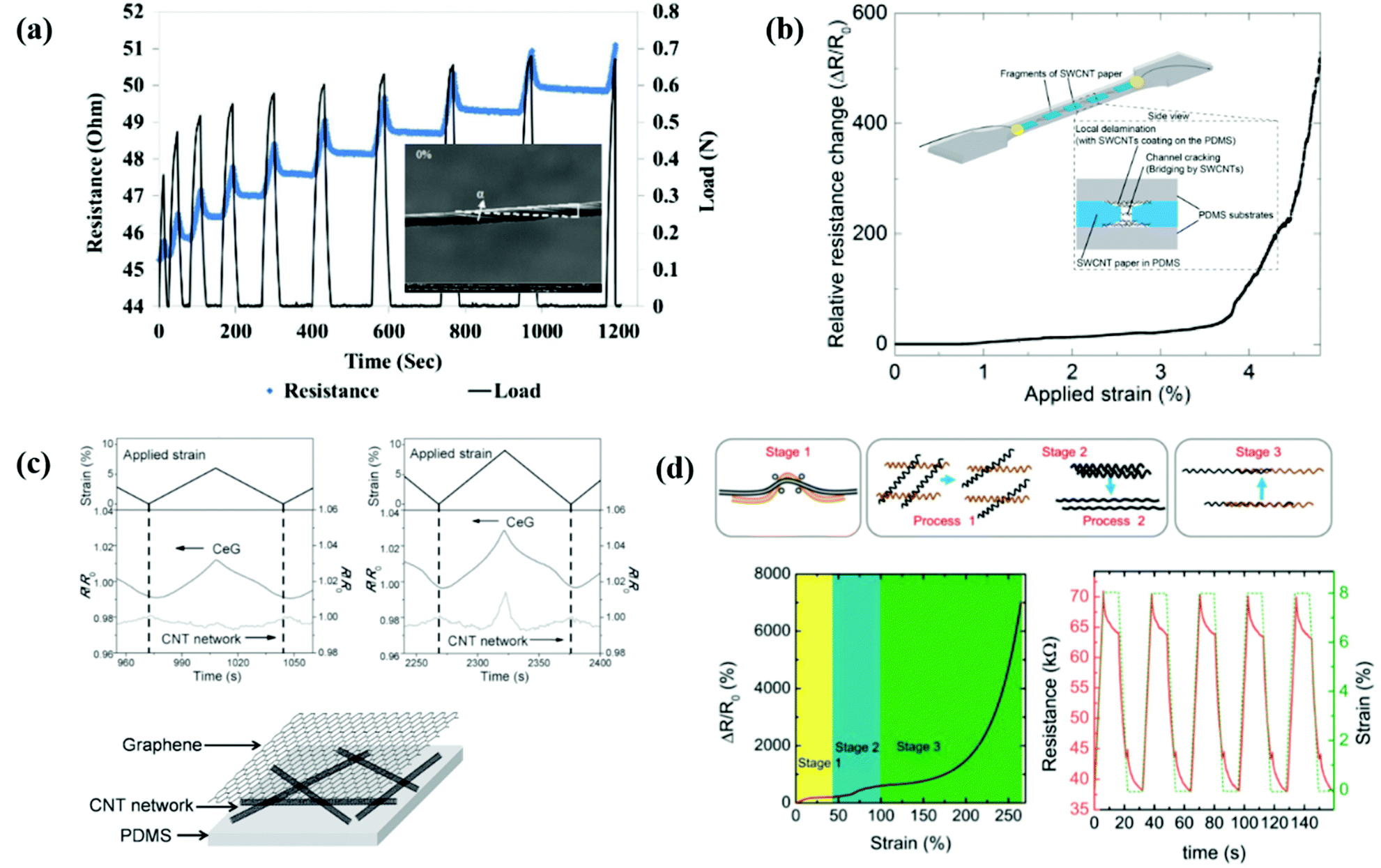 | ||
| Fig. 7 Applications of CNT fibers and films in stretchable electronics. (a) Corresponding real time resistance and tensile loading. The inset is a SEM image of a CNT yarn. Adapted and modified with permission from ref. 104. Copyright 2015, Elsevier Ltd. (b) Relative resistance change of CNT paper under different tensile strains. The inset is the illustration of the fragmental structure in CNT paper at the stretching state. Adapted and modified with permission from ref. 105. Copyright 2017, American Chemical Society. (c) Plots of a triangle test with the peak strain of 6% (left) and 9% (right). The illustration is a schematic of a layered CNT–graphene hybrid. Adapted and modified with permission from ref. 19. Copyright 2016, Wiley-VCH. (d) Schematic of the structural changes under different degrees of tension (up). Resistance change ratio as a function of different tensile strains and change in resistance under repeated stretching–releasing cycles (down). Adapted and modified with permission from ref. 106. Copyright 2017, The Royal Society of Chemistry. | ||
Deng et al. developed a quite sensitive strain sensor based on carbon nanocoils (CNCs) by a peeling-off approach.106 The sensor with super stretchability could detect tiny tensile strain of about 0.001% and large strain of 260%. The resistance change curve can be divided into three stages, corresponding to the structural change caused by the unique spring-like morphology in three stages (Fig. 7d). The sensor also had the ability to detect bend and compression, showing its wide potential applications.
Ryu et al. demonstrated that an intrinsically stretchable multi-functional fiber was able to harvest mechanical energy and detect strain simultaneously.107 The fiber with a hollow cylindrical structure was composed of PDMS, composite of MWCNTs and poly(3,4-ethylenedioxythiophene)polystyrene sulfonate (PEDOT:PSS), composite of spherical P(VDF-TrFE) and PDMS, composite of MWCNTs and PEDOT:PSS, and PDMS from outside to inside in the transverse section (Fig. 8a). The conductivity of the MWCNT layers was distinctly enhanced after the mixture of PEDOT:PSS. Due to piezoelectricity, an output voltage was generated between two composite layers of PEDOT:PSS and MWCNTs by repeatedly stretching and releasing the fiber with a strain of 50%. The magnitude of the voltage increased with the stretching and releasing rate (Fig. 8b). The stretchable fiber could also be used as a strain sensor. The resistance of the composite layer of PEDOT:PSS and MWCNTs increased with increasing tensile strain. Meanwhile, invariable baseline resistance after 1000 cycles of 50% strain proved the robustness of the fiber applied in tensile sensors (Fig. 8c).
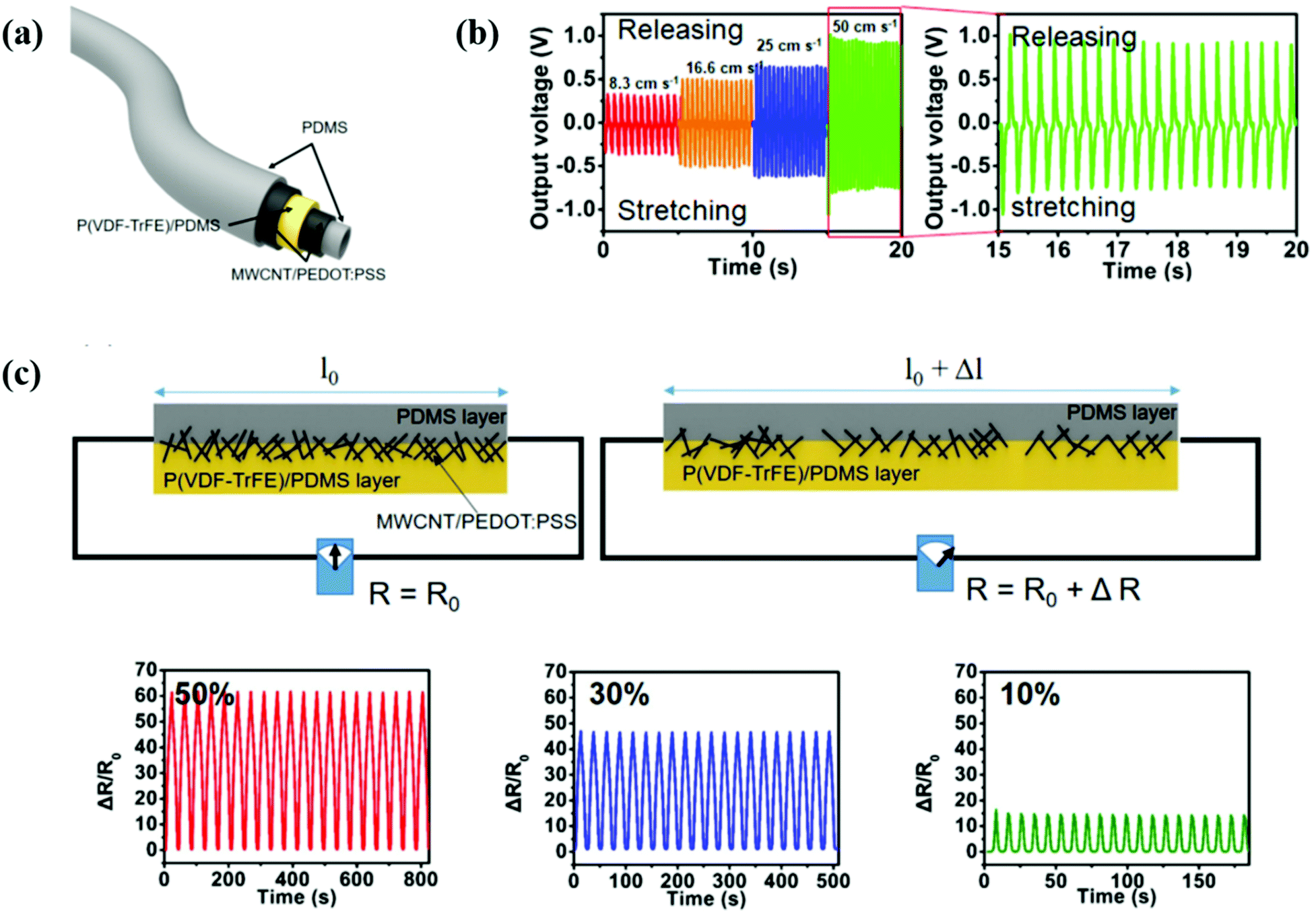 | ||
| Fig. 8 Applications of CNTs in energy harvesters. (a) Schematic of a intrinsically stretchable multi-functional fiber. (b) Generated voltage from the fiber under repeated stretching–releasing cycles at different strain rates. (c) Simplified schematic of the strain-sensing principle and relative change ratio of fiber resistance under repeated stretching–releasing cycles at different strains (down). Adapted and modified with permission from ref. 107. Copyright 2019, Elsevier Ltd. | ||
5. Conducting polymers
In 1977, the first conducting polymer, doped polyacetylene with a conductivity of 103 S cm−1, was reported by H. Shirakawa.108,109 Since then, conductive polymers as emerging intrinsically stretchable conductors have received increased attention. The most widely known conducting polymers are polyaniline (PANi), polypyrrole (PPy), polythiophene (PTh), poly(3,4-ethylenedioxythiophene) (PEDOT), and their derivatives. To date, there has not yet been a coherent hypothesis to explain the relationship between morphology, chain structure and conductivity. A contiguous sp2 hybridized carbon center is a typical structure existing in some conducting polymers. Thus, a conjugated π bond is often used to describe the conductive behavior in polymers. Undoped conjugated polymers are often semiconductors or insulators. Similar to silicon semiconductors, conjugated polymers show conductive characteristics of n- or p-type semiconductors by means of reduction, oxidization or doping of protic solvents.Recently, researchers have designed a new type of stretchable conductive polymer with a double network (DN) structure. The conductive elastomers were fabricated with dual physically cross-linked DN and ionic cross-linking. The DN structure generally consisted of hard and soft polymers, which were bonded by crosslinks. The unique fully physically cross-linked structure endowed the polymers with good stretchability, low Young's modulus and outstanding fatigue resistance. Meanwhile, the ion doping effectively improved the ionic conductivity of the polymers, which was different from the conductive property of conjugated polymers via electronic transport (Fig. 9).30,110–113 Based on the DN structure, polymers with self-healing properties could be used to prepare stretchable conductive electrodes. Not only the morphological integrity of the polymers, but the conductivity also exhibited a high self-healing efficiency (Fig. 10).114–116
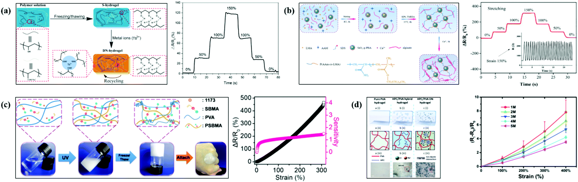 | ||
| Fig. 9 Applications of conducting polymers with a DN structure in stretchable electronics. (a) Schematic of the preparation procedure and the network structure of DN-hydrogels (left) and the relative change in resistance (right). Adapted and modified with permission from ref. 30. Copyright 2018, The Royal Society of Chemistry. (b) Schematic of the preparation procedure of DN-hydrogels (left) and the relative resistance under different tensile strains (right). Adapted and modified with permission from ref. 110. Copyright 2018, Elsevier Ltd. (c) Schematic and optical images of the preparation procedure of a synthetic ionic gel (left) and resistance change ratio and sensitivity of the hydrogel under tensile strain (right). Adapted and modified with permission from ref. 111. Copyright 2019, The Royal Society of Chemistry. (d) Schematic design, microstructure and optical image of different PVA hydrogels (left) and resistance change ratio of hydrogels under tensile strain (right). Adapted and modified with permission from ref. 112. Copyright 2018, Wiley-VCH. | ||
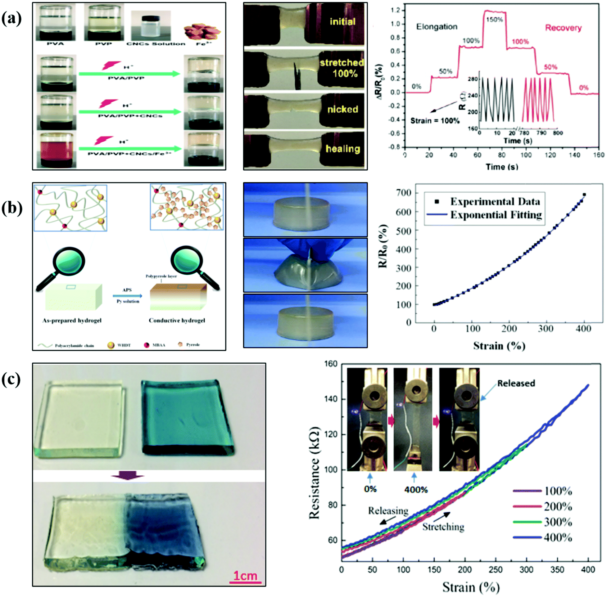 | ||
| Fig. 10 Applications of conducting polymers with self-healing ability in stretchable electronics. (a) Schematic of the preparation of functional network hydrogels (left), self-healing capability for elastic hydrogels (middle) and the relative resistance under different tensile strains (right). Adapted and modified with permission from ref. 115. Copyright 2017, American Chemical Society. (b) Schematic of polyacrylamide hydrogels and polypyrrole-based conductive hydrogels (left), the photographs of the deformation of conductive hydrogels under sliced conditions and their recovery to the original state (middle) and the relationship between the relative resistance and the tensile strain (right). Adapted and modified with permission from ref. 114. Copyright 2018, The Royal Society of Chemistry. (c) A freshly cut DN hydrogel with a sheet shape and the self-healed sheet-shaped sample (left) and the change in resistance under stretching–releasing cycles (right). Adapted and modified with permission from ref. 116. Copyright 2017, American Chemical Society. | ||
Over the past four decades, conductive polymers have attained much progress from molecule design, material synthesis, doping, and conductive mechanism towards processability and stability. PEDOT:PSS is the most successful commercially available aqueous dispersion of conductive polymers. Even so, instability in atmospheric moisture and poor processability are still the main barriers to further applications of conductive polymers, especially conjugated polymers. In addition, it is also a major challenge to maintain the excellent electrical and mechanical properties of the conductive polymers.
6. Conductive composites
6.1. Concept of percolation
Different from the above intrinsically stretchable conductors, stretchable conductive composites were typically fabricated by embedding solid conductive fillers into an elastomeric matrix. This strategy has greatly enriched both the scope of selectable materials and the application of the stretchable conductive materials. The volume fraction of conductive fillers in the matrix plays a main role in the conductivity and stretchability of the composite. Percolation theory, describing the behavior of interconnected clusters in a random graph, is often used to predict and analyze the conductivity of stretchable conductive composites.Fig. 11a shows a typical curve of composite conductivity as a function of volume fraction of conductive fillers. Percolation threshold, the most important concept in percolation theory, represents the critical value of volume fraction of conductive fillers required to form continuous electrical pathways in a given polymer matrix. If the volume fraction of fillers is low enough, none of the electrical pathways exists in the composite due to the separated conductive fillers (part 1 in Fig. 11a). Then, the conductivity of the composite increases by several orders of magnitude with the volume fraction of fillers beyond the percolation threshold (part 2 in Fig. 11a). When the volume fraction is much larger than the percolation threshold, the conductivity rises steadily owing to the formation of several conductive pathways in the composite (part 3 in Fig. 11a).
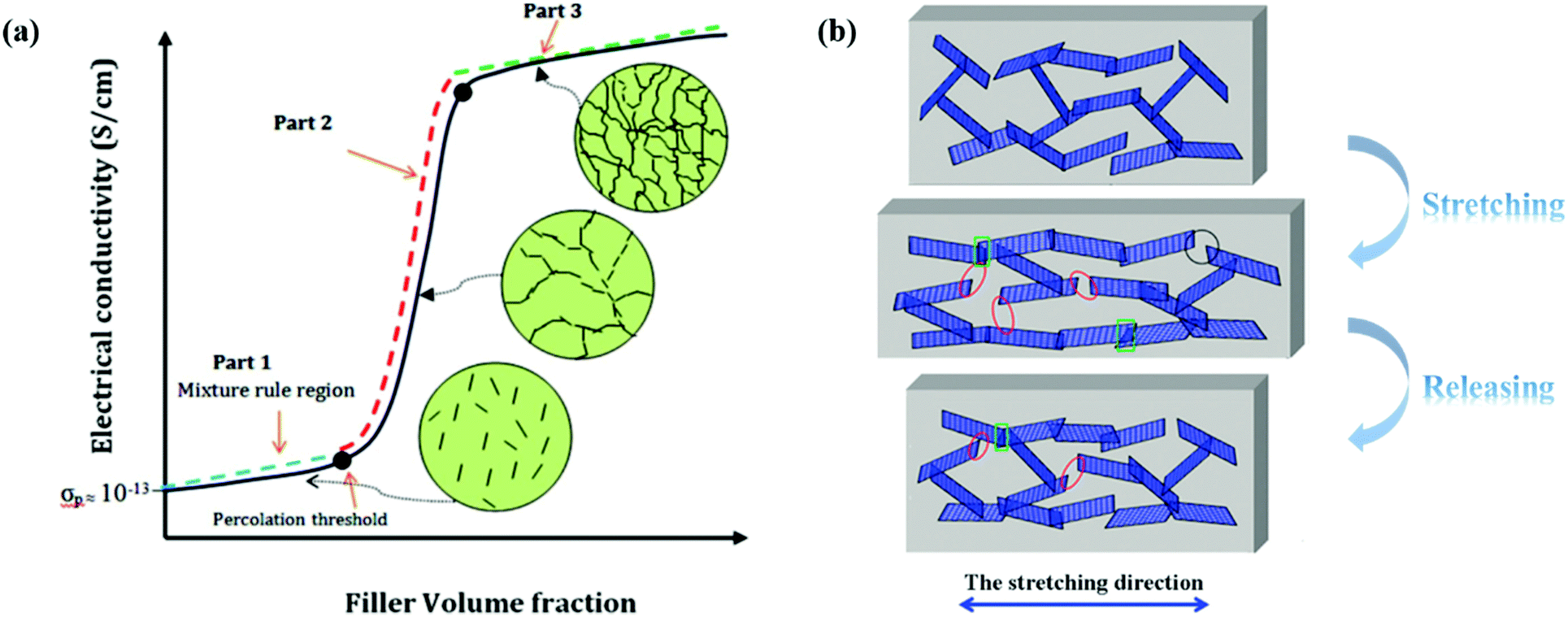 | ||
| Fig. 11 (a) Typical behavior of composite conductivity as a function of filler volume fraction. Adapted and modified with permission from ref. 117. Copyright 2014, the electrochemical society. (b) Schematic of the structural evolution of a graphene network during a stretching–releasing cycle. Adapted and modified with permission from ref. 47. Copyright 2016, The Royal Society of Chemistry. | ||
To date, a mass of models have been established to describe the electrical characteristics of 2D and 3D percolation networks composed of conductive nanomaterials in a polymer matrix. The following proportional relationship is typically used to investigate the sharp change in conductivity near the percolation threshold:
| σ ∝ (φ − φc)n | (1) |
The existing results show that the percolation threshold is mainly influenced by species, geometrical factors, and orientations of conductive fillers with an ideal dispersion in a polymer matrix. In a given system, an increase in volume fraction of the conductive filler is able to improve the conductivity of the composite, but also simultaneously leads to a reduction of its stretchability. Therefore, the choice of an appropriate conductive filler with low percolation threshold is very important to produce highly conductive nanocomposites for stretchable devices. A perfect design of device can realize the full potential of a certain conductive filler.
Electron transportation between adjacent conductive fillers is usually described by the tunneling model. Besides the electronic energy levels of adjacent conductive fillers, the contact area and distance between them also determine the interfacial resistance. Fig. 11b illustrates the change of a graphene network in a stretching–releasing process. Under tensile strain, the conductive fillers are dragged along the stretching direction by polymer chains due to the intermolecular interactions between the matrix and fillers. It leads to the damage of electron transport pathways, further resulting in an increase of composite volume resistance. After removing the stretching loading, the conductivity is recovered with the reconstruction of the pathways between adjacent conductive fillers. It is worth noting that the irreversible resistance at the releasing state derives from the permanent structural damage, including the irreversible strain of the polymer and the change in conductive pathways.
6.2. Conductive composites filled with metallic nanoparticles
The typical method for forming an isotropic 3D percolation network is the homogeneous distribution of the conductive fillers into a polymer matrix, which has isotropic conductivity and stretchability.43 To further increase the stretchability, a variety of structural designs and preparative methods have also been attempted. Chun et al. synthesized a stretchable and conductive composite film from Ag flakes, Ag nanoparticle (NP) coated CNTs and a polymer matrix.118,119 As shown in Fig. 12a, the reduction in conductivity of the composites with different concentrations of Ag flakes was less than one order of magnitude. Among them, the conductivity of composites with 8.6 wt% Ag flakes was about 706 S cm−1 under a 30% tensile strain. After 5000 repeated stretching–releasing cycles, the conductivity of the composite at the releasing state was a stable value of 1510 S cm−1.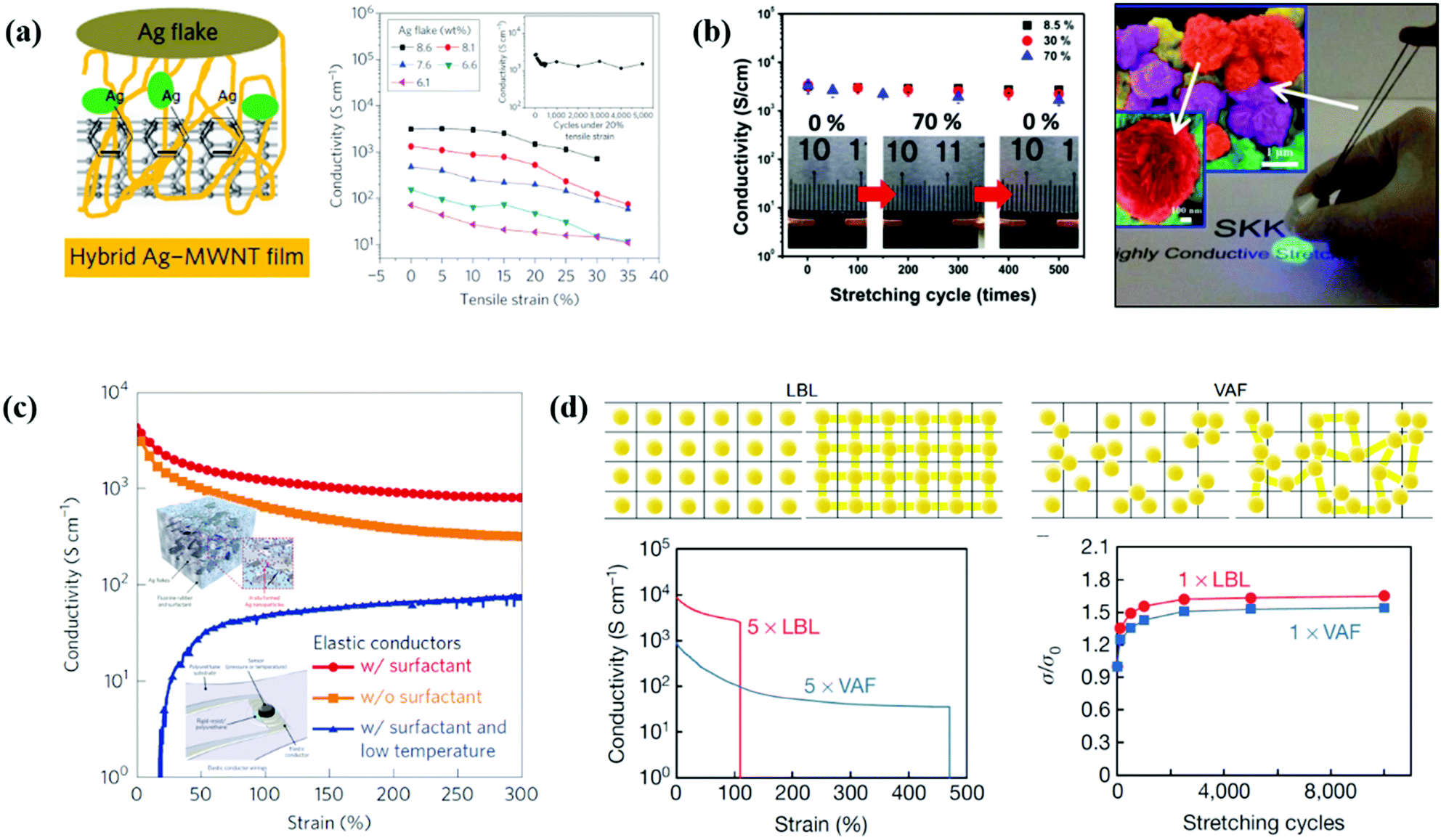 | ||
| Fig. 12 Composites made of metallic NPs or flakes used as stretchable electrodes. (a) Schematic of the preparation of a hybrid Ag-MWCNT composite film (left) and conductivity of the hybrid Ag-MWCNT composite film under different tensile strains (right). Adapted and modified with permission from ref. 118. Copyright 2010, Nature Publishing Group. (b) Change in conductivity of the Ag–PU fiber under stretching–releasing cycles (left) and a light-emitting diode connected to two conductors knitted from Ag–PU fibers (right). Adapted and modified with permission from ref. 3. Copyright 2015, American Chemical Society. (c) Change in conductivity of different elastic conductors under tensile strain. The insets are the schematic of in situ formed Ag nanoparticles from Ag flakes in composites and the structure of the sensor. Adapted and modified with permission from ref. 128. Copyright 2017, Nature Publishing Group. (d) Schematic of well-dispersed Au NPs in LBL and VAF composites (up). Conductivity of LBL and VAF sheets under different tensile strains and relative change in resistance under repeated stretching–releasing cycles (down). Adapted and modified with permission from ref. 120. Copyright 2013, Nature Publishing Group. | ||
Ma et al. prepared a stretchable electrode with outstanding conductivity and mechanical strength by the combination of Ag nanoflowers (NFs) and PU.3 The enhanced surface area from the petals of Ag NFs was beneficial for the formation of more conductive pathways. With a moderate volume fraction of Ag NFs and curing temperature of composites, the initial conductivity and maximum tensile strain of Ag–PU fibers could reach 41245 S cm−1 and 776%, respectively. The maximum Young's modulus and ultimate strength were also improved up to 731.5 and 39.6 MPa compared with Ag PVDF-HFP fibers. After the pre-stretching cycle, the fiber exhibited an excellent elastic behavior during the repeated stretching–releasing cycles. There was a negligible decay of conductivity when the strain was less than 30%. The conductors based on Ag–PU fibers were used to connect an LED and an electric source. The brightness of the LED was maintained due to the high conductivity of fibers under the stretching state of conductors (Fig. 12b). Matsuhisa et al. prepared stretchable conductors by a printing method from an ink comprising fluorine rubber, fluorine surfactant, Ag flakes, and methylisobutylketone (MIBK) as the solvent. It was found that abundant Ag NPs in situ formed in the composites after printing and heating. The dispersed Ag NPs improved percolation between Ag flakes and suppressed crack formation, resulting in the enhancement of the electrical and mechanical properties of the composites (Fig. 12c).
Kim et al. prepared stretchable conductors composed of Au spherical NPs and PU by the layer-by-layer (LBL) method and vacuum-assisted flocculation (VAF).120 The films prepared by the two methods exhibited distinctly different properties even when the concentration of Au NPs was the same. The LBL composites had more efficient conductive pathways due to better dispersed NPs, compared with VAF films. However, the stretchability of the VAF films was better than that of the LBL films. The experimental results demonstrated that the initial conductivity of LBL and VAF films with five sheets was 11000 S cm−1 and 1800 S cm−1, and the maximum tensile strain was 115% and 486%, respectively (Fig. 12d). After 10000 repeated stretching–releasing cycles of 5% strain, the resistance increase of both LBL and VAF films was around 50%.
6.3. Conductive composites filled with carbon materials
Various carbon materials are also used as conductive fillers embedded into polymers. Compared with metallic NPs, the low mass density of carbon materials is beneficial for lightweight of stretchable electronic devices. Li et al. fabricated a multifunctional composite by using MWCNTs as the conductive network and a highly elastic form-stable phase change polymer (HEPCP) as the elastic substrate.23 Due to the cyclic and reversible changes in the MWCNT conductive network, the composite exhibited high sensitivity to infrared radiation (IR) illumination, temperature change, and tensile strain (Fig. 13a).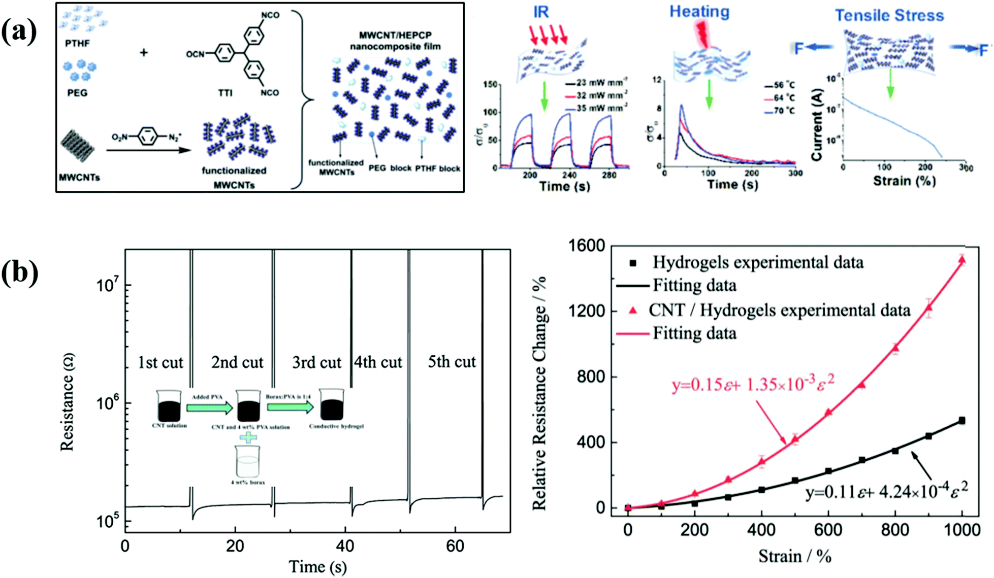 | ||
| Fig. 13 Applications of CNT-based composites in stretchable electronics. (a) Schematic of the synthesis process for the MWCNT/HEPCP composites (left) and electric response of the composite film to infrared illumination, temperature and tensile strain (right). Adapted and modified with permission from ref. 23. Copyright 2018, The Royal Society of Chemistry. (b) Change in resistance of the composite under the repeated cutting–healing process at the same location (left), change ratio of resistance under different tensile strains (middle) and change ratio of resistance for various human motions (right). The inset is the schematic of the fabrication process of the conductive composite. Adapted and modified with permission from ref. 121. Copyright 2016, Wiley-VCH. | ||
Self-healing is another important feature of artificial electronic skin. The Bao group fabricated a self-healing electronic skin based on NP-supramolecular organic composites and the percolation network was repaired with the self-healing of the matrix.24 Cai et al. prepared an extremely stretchable strain sensor based on a CNT/polyvinyl alcohol (PVA)/borax conductive hydrogel.121 Due to the existence of extensive hydrogen-bonding between the tetrafunctional borate ion and -OH group in the PVA/borax hydrogel, the composite was easily broken and re-formed. The conductive hydrogel exhibited a stretchable deformation (up to 1000%), fast electrical healing speed (within 3.2 s), and high self-healing efficiency (98 ± 0.8%). Even though the sensor based on the CNT/PVA/borax hydrogel underwent 700% stretching strain for 1000 cycles, there was no significant change observed in the intrinsic properties (Fig. 13b). The self-healing materials provided a wide range of applications in health monitoring, bionic devices, and medical treatments.
Carbon blacks (CBs) could also be used as conductive fillers to prepare stretchable and conductive composites. Chun et al. developed a stretchable conductive carbon composite with octopus-like patterns (OP) capable of attaching onto the skin and resisting water.122 The unique protuberance-like dome-shaped structures enabled the composite to tightly attach onto various substrates in a dry or wet environment. Normal adhesion strengths for the OP-CPC film on a skin replica both under dry and underwater conditions were larger than 1 N cm−2. The experimental results showed that the OP-CPC film was a stretchable conductor due to percolation networks of CB in the film. In particular for the 7.0 vol% film, there was a negligible change in resistance under a tensile strain of 60% (Fig. 14a). A test of 10000 repeated stretching–releasing cycles confirmed the robustness of the OP-CPC composites. A device composed of OP-CPC with 7 vol% CB as the stretchable electrode was fabricated to monitor brachial nerves. The signals appeared to be of almost the same waveform, while the wrist bent at different angles. This work built a promising route to meet the requirements in attachable biomedical devices. Boland et al. also tried to embed graphene flakes into a highly viscoelastic putty. The percolation threshold was at the volume fraction of 1.75% deduced from percolation theory. For the volume fraction of 6.8%, the change ratio of resistance gradually increased under a tensile strain lower than 1% and decreased rapidly under higher strain. The nonmonotonic changes in resistance with strain were associated with the movement of nanosheets in the low-viscosity putty matrix (Fig. 14b). The network was relaxed slowly and the resistance was decreased by connection re-formation due to the low matrix viscosity. This relaxation behavior was considered as a self-healing process in the report.
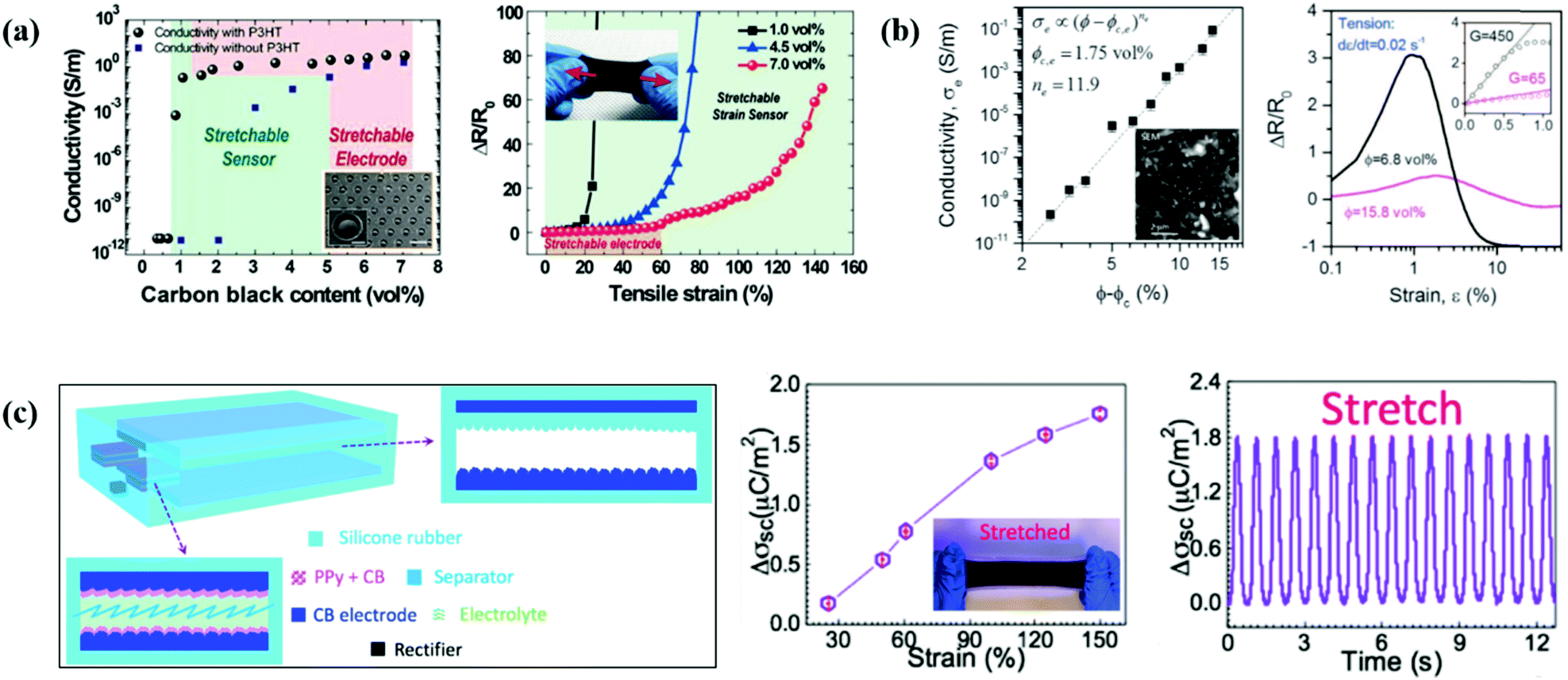 | ||
| Fig. 14 Applications of carbon material-based composites in stretchable electronics. (a) Change ratio of resistance under different tensile strains (left) and electric signals of OP-CPC electronics in dry and wet environments for different actions of the wrist (right). The inset is the SEM image of the protuberance-like dome-shaped structures on the surface of an octopus-inspired carbon-based conductive composite. Adapted and modified with permission from ref. 122. Copyright 2018, Wiley-VCH. (b) Conductivity of graphene-based putty (G-putty) as a function of volume fraction of reduced graphene (left) and change in resistance of the G-putty under different tensile strains (right). The inset is the SEM image of the surface of the G-putty. Adapted and modified with permission from ref. 16. Copyright 2016, American Association for the Advancement of Science. (c) Schematic of a stretchable self-charging power system (left). Relationship between short-circuit transferred charge density (Δσsc) and the tensile strain of the device (middle) and Δσsc of the device under repeated stretching–releasing cycles (right). Adapted and modified with permission from ref. 127. Copyright 2016, American Chemical Society. | ||
Since 2006, the Wang group has developed a series of flexible nanogenerators based on piezoelectricity and triboelectricity.25,123–126Fig. 14c represents a type of stretchable and fully enclosed self-charging power system, which integrated a stretchable triboelectric nanogenerator (TENG) for converting mechanical energy into electricity and a stretchable supercapacitor for storing electricity.127 The experimental results showed that the short-circuit transferred charge density of the device gradually increased with stretching strain, and the output signal was almost unchanged under repeated stretching–releasing cycles. In addition, the capacitance of the device reduced from 2.3 mF to 2.0 mF, while the stretching strain was 100%. Such a self-sustainable energy generator is conducive to realizing wearable electronics and bioelectronics without an external power supply.
7. Conclusions
Intrinsically stretchable conductors with high conductivity and stretchability have been employed to develop novel soft electronic devices and systems. Stretchability is an intrinsic property, which is not obtained by structural design of patterning. The properties of the selected stretchable conductors determine the performance of the integrated devices and systems. Metallic nanomaterials, liquid metals, carbon nanomaterials, conducting polymers, and conductive composites are the main categories of intrinsically stretchable and conductive materials.Compared with metallic blocks, 1D metallic NWs and nanotroughs improve the stretchability and maintain the conductivity. The biggest challenge in the networks composed of metallic NWs or nanotroughs used as transparent and stretchable electrodes is the weak contact of junctions, which lowers their mechanical strength and conductivity. Various welding technologies have been developed to improve the point contact at NW–NW junctions.
In theory, liquid metals have the ability to extend infinitely due to their unique fluidity. However, they must be fully encapsulated in sealed elastomers when they are used in electrical devices. In addition, disadvantages such as toxicity, low conductivity compared with metals, low manufacturability and wetting properties, may limit the applications of liquid metals in the future.
Carbon nanomaterials are another class of stretchable and conductive materials. Similar to metallic NWs and nanotroughs, extensive contact interfaces directly determine the mechanical and electrical properties of assembled networks. Moreover, most of the carbon nanomaterials are light-weight. They also have outstanding flexibility and stretchability. These special characteristics are suitable in wearable and light-weight devices.
Conducting polymers as stretchable conductors in nature have better stretchability compared with metallic and carbon nanomaterials. However, low conductivity is the biggest barrier to their application in stretchable conductors. This disadvantage has been overcome partially by ion doping and blending modifications. Even so, it is still a major challenge to simultaneously maintain good electrical and mechanical properties of the conductive polymers.
Stretchable conductive composites play a considerable role in the development of intrinsically stretchable and conductive materials. By embedding various conductive fillers in a polymer matrix, the composites are enabled to exhibit both conductivity and stretchability. To date, researchers have developed a variety of stretchable and conductive composites with other properties, such as self-healing, shape memory, and conductive sensitivity to different external stimuli. They have been widely used in wearable devices, multifunctional sensors, energy harvesters, and biomedical fields. However, the optimization of the volume fraction of conductive fillers is a key factor to obtain the desired mechanical and electrical properties for intrinsically stretchable conductive composites.
Conflicts of interest
There are no conflicts to declare.Acknowledgements
The authors wish to acknowledge financial support from MoST (2016YFA0200200), NSFC (21875114) and the ‘‘111 Project’’ of China (B18030).Notes and references
- D. Chen, J. Liang and Q. Pei, Sci. China: Chem., 2016, 59, 659–671 CrossRef CAS.
- R. Ma, J. Lee, D. Choi, H. Moon and S. Baik, Nano Lett., 2014, 14, 1944–1951 CrossRef CAS PubMed.
- R. Ma, B. Kang, S. Cho, M. Choi and S. Baik, ACS Nano, 2015, 9, 10876–10886 CrossRef CAS PubMed.
- J. Liang, L. Li, X. Niu, Z. Yu and Q. Pei, Nat. Photonics, 2013, 7, 817–824 CrossRef CAS.
- J. H. Koo, D. C. Kim, H. J. Shim, T. Kim and D. Kim, Adv. Funct. Mater., 2018, 28, 1801834 CrossRef.
- U. Kim, J. Kang, C. Lee, H. Y. Kwon, S. Hwang, H. Moon, J. C. Koo, J. D. Nam, B. H. Hong, J. B. Choi and H. R. Choi, Nanotechnology, 2013, 24, 145501 CrossRef PubMed.
- C. Wu, J. Feng, L. Peng, Y. Ni, H. Liang, L. He and Y. Xie, J. Mater. Chem., 2011, 21, 18584–18591 RSC.
- S. Liang, X. Qiu, J. Yuan, W. Huang, X. Du and L. Zhang, ACS Appl. Mater. Interfaces, 2018, 10, 19123–19132 CrossRef CAS PubMed.
- D. Han, Y. Zhang, Y. Liu, Y. Liu, H. Jiang, B. Han, X. Fu, H. Ding, H. Xu and H. Sun, Adv. Funct. Mater., 2015, 25, 4548–4557 CrossRef CAS.
- M. Ji, N. Jiang, J. Chang and J. Sun, Adv. Funct. Mater., 2014, 24, 5412–5419 CrossRef CAS.
- C. Wang, Y. Wang, Y. Yao, W. Luo, J. Wan, J. Dai, E. Hitz, K. K. Fu and L. Hu, Adv. Mater., 2016, 28, 8618–8624 CrossRef CAS PubMed.
- M. Ji, N. Jiang, J. Chang and J. Sun, Adv. Funct. Mater., 2014, 24, 5412–5419 CrossRef CAS.
- F. Ge and Y. Zhao, Chem. Sci., 2017, 8, 6307–6312 RSC.
- E. Acome, S. K. Mitchell, T. G. Morrissey, M. B. Emmett, C. Benjamin, M. King, M. Radakovitz and C. Keplinger, Science, 2018, 359, 61–65 CrossRef CAS PubMed.
- Y. Qin, Q. Peng, Y. Ding, Z. Lin, C. Wang, Y. Li, F. Xu, J. Li, Y. Yuan, X. He and Y. Li, ACS Nano, 2015, 9, 8933–8941 CrossRef CAS PubMed.
- C. S. Boland, U. Khan, G. Ryan, S. Barwich, R. Charifou, A. Harvey, C. Backes, Z. Li, M. S. Ferreira, M. E. M. Bius, R. J. Young and J. N. Coleman, Science, 2016, 354, 1257–1260 CrossRef CAS PubMed.
- Z. Yang, Y. Pang, X. Han, Y. Yang, J. Ling, M. Jian, Y. Zhang, Y. Yang and T. Ren, ACS Nano, 2018, 12, 9134–9141 CrossRef CAS PubMed.
- Y. Cheng, R. Wang, J. Sun and L. Gao, Adv. Mater., 2015, 27, 7365–7371 CrossRef CAS PubMed.
- J. Shi, X. Li, H. Cheng, Z. Liu, L. Zhao, T. Yang, Z. Dai, Z. Cheng, E. Shi, L. Yang, Z. Zhang, A. Cao, H. Zhu and Y. Fang, Adv. Funct. Mater., 2016, 26, 2078–2084 CrossRef CAS.
- Q. Cao and J. A. Rogers, Adv. Mater., 2009, 21, 29–53 CrossRef CAS.
- Y. Yu, Y. Luo, A. Guo, L. Yan, Y. Wu, K. Jiang, Q. Li, S. Fan and J. Wang, Nanoscale, 2017, 9, 6716–6723 RSC.
- K. Chen, W. Gao, S. Emaminejad, D. Kiriya, H. Ota, H. Y. Y. Nyein, K. Takei and A. Javey, Adv. Mater., 2016, 28, 4397–4414 CrossRef CAS PubMed.
- M. Li, Y. Wang, Y. Zhang, H. Zhou, Z. Huang and D. Li, J. Mater. Chem. C, 2018, 6, 5877–5887 RSC.
- D. Son, J. Kang, O. Vardoulis, Y. Kim, N. Matsuhisa, J. Y. Oh, J. W. To, J. Mun, T. Katsumata, Y. Liu, A. F. McGuire, M. Krason, F. Molina-Lopez, J. Ham, U. Kraft, Y. Lee, Y. Yun, J. B. H. Tok and Z. Bao, Nat. Nanotechnol., 2018, 13, 1057–1065 CrossRef CAS PubMed.
- K. Dong, Z. Wu, J. Deng, A. C. Wang, H. Zou, C. Chen, D. Hu, B. Gu, B. Sun and Z. L. Wang, Adv. Mater., 2018, 30, 1804944 CrossRef PubMed.
- Z. Ma, S. Li, H. Wang, W. Cheng, Y. Li, L. Pan and Y. Shi, J. Mater. Chem. B, 2019, 7, 173–197 RSC.
- A. Chortos, G. I. Koleilat, R. Pfattner, D. Kong, P. Lin, R. Nur, T. Lei, H. Wang, N. Liu, Y. Lai, M. Kim, J. W. Chung, S. Lee and Z. Bao, Adv. Mater., 2016, 28, 4441–4448 CrossRef CAS PubMed.
- J. Mun, G. N. Wang, J. Y. Oh, T. Katsumata, F. L. Lee, J. Kang, H. Wu, F. Lissel, S. Rondeau-Gagné, J. B. H. Tok and Z. Bao, Adv. Funct. Mater., 2018, 28, 1804222 CrossRef.
- H. Wu, S. J. Benight, A. Chortos, W. Lee, J. Mei, J. W. F. To, C. Lu, M. He, J. B. H. Tok, W. Chen and Z. Bao, Chem. Mater., 2014, 26, 4544–4551 CrossRef CAS.
- J. Lai, H. Zhou, M. Wang, Y. Chen, Z. Jin, S. Li, J. Yang, X. Jin, H. Liu and W. Zhao, J. Mater. Chem. C, 2018, 6, 13316–13324 RSC.
- R. Ma, S. Kwon, Q. Zheng, H. Y. Kwon, J. I. Kim, H. R. Choi and S. Baik, Adv. Mater., 2012, 24, 3344–3349 CrossRef CAS PubMed.
- S. Ryu, P. Lee, J. B. Chou, R. Xu, R. Zhao, A. J. Hart and S. Kim, ACS Nano, 2015, 9, 5929–5936 CrossRef CAS PubMed.
- Y. Liu, L. Tao, D. Wang, T. Zhang, Y. Yang and T. Ren, Appl. Phys. Lett., 2017, 110, 123508 CrossRef.
- R. Rahimi, M. Ochoa, A. Tamayol, S. Khalili, A. Khademhosseini and B. Ziaie, ACS Appl. Mater. Interfaces, 2017, 9, 9015–9023 CrossRef CAS PubMed.
- H. Lee, I. Kim, M. Kim and H. Lee, Nanoscale, 2016, 8, 1789–1822 RSC.
- H. Jin, N. Matsuhisa, S. Lee, M. Abbas, T. Yokota and T. Someya, Adv. Mater., 2017, 29, 1605848 CrossRef PubMed.
- A. M. Hussain, F. A. Ghaffar, S. I. Park, J. A. Rogers, A. Shamim and M. M. Hussain, Adv. Funct. Mater., 2015, 25, 6565–6575 CrossRef CAS.
- T. Sekitani and T. Someya, Adv. Mater., 2010, 22, 2228–2246 CrossRef CAS PubMed.
- Y. Yu, C. Yan and Z. Zheng, Adv. Mater., 2014, 26, 5508–5516 CrossRef CAS PubMed.
- F. Bossuyt, T. Vervust and J. Vanfleteren, IEEE Trans. Compon., Packag., Manuf. Technol., 2013, 3, 229–235 Search PubMed.
- Y. Zhang, S. Wang, X. Li, J. A. Fan, S. Xu, Y. M. Song, K. Choi, W. Yeo, W. Lee, S. N. Nazaar, B. Lu, L. Yin, K. Hwang, J. A. Rogers and Y. Huang, Adv. Funct. Mater., 2014, 24, 2028–2037 CrossRef CAS.
- J. Ahn and J. H. Je, J. Phys. D: Appl. Phys., 2012, 45, 103001 CrossRef.
- Y. Zhao, D. Dong, S. Gong, L. Brassart, Y. Wang, T. An and W. Cheng, Adv. Electron. Mater., 2018, 5, 1800462 CrossRef.
- C. Cao, Y. Chu, Y. Zhou, C. Zhang and S. Qu, Small, 2018, 14, 1803976 CrossRef PubMed.
- S. Park, M. Vosguerichian and Z. Bao, Nanoscale, 2013, 5, 1727–1752 RSC.
- G. N. Wang, A. Gasperini and Z. Bao, Adv. Electron. Mater., 2018, 4, 1700429 CrossRef.
- H. Liu, Y. Li, K. Dai, G. Zheng, C. Liu, C. Shen, X. Yan, J. Guo and Z. Guo, J. Mater. Chem. C, 2016, 4, 157–166 RSC.
- H. J. Kim, K. Sim, A. Thukral and C. Yu, Sci. Adv., 2017, 3, e1701114 CrossRef PubMed.
- Y. Kim, A. Chortos, W. Xu, Y. Liu, J. Y. Oh, D. Son, J. Kang, A. M. Foudeh, C. Zhu, Y. Lee, S. Niu, J. Liu, R. Pfattner, Z. Bao and T. Lee, Science, 2018, 360, 998–1003 CrossRef CAS PubMed.
- S. Choi, S. I. Han, D. Kim, T. Hyeon and D. Kim, Chem. Soc. Rev., 2019, 48, 1566–1595 RSC.
- R. Ma, S. Chou, Y. Xie and Q. Pei, Chem. Soc. Rev., 2019, 48, 1741–1786 RSC.
- C. S. Boland, U. Khan, C. Backes, A. O'Neill, J. McCauley, S. Duane, R. Shanker, Y. Liu, I. Jurewicz, A. B. Dalton and J. N. Coleman, ACS Nano, 2014, 8, 8819–8830 CrossRef CAS PubMed.
- D. W. Pashley, Proc. R. Soc. London, Ser. A, 1960, 255, 218–231 CAS.
- H. Wu, D. Kong, Z. Ruan, P. Hsu, S. Wang, Z. Yu, T. J. Carney, L. Hu, S. Fan and Y. Cui, Nat. Nanotechnol., 2013, 8, 421–425 CrossRef CAS PubMed.
- S. Soltanian, R. Rahmanian, B. Gholamkhass, N. M. Kiasari, F. Ko and P. Servati, Adv. Energy Mater., 2013, 3, 1332–1337 CrossRef CAS.
- T. Tokuno, M. Nogi, M. Karakawa, J. Jiu, T. T. Nge, Y. Aso and K. Suganuma, Nano Res., 2011, 4, 1215–1222 CrossRef CAS.
- E. C. Garnett, W. Cai, J. J. Cha, F. Mahmood, S. T. Connor, M. Greyson Christoforo, Y. Cui, M. D. McGehee and M. L. Brongersma, Nat. Mater., 2012, 11, 241–249 CrossRef CAS PubMed.
- S. Han, S. Hong, J. Ham, J. Yeo, J. Lee, B. Kang, P. Lee, J. Kwon, S. S. Lee, M. Yang and S. H. Ko, Adv. Mater., 2014, 26, 5808–5814 CrossRef CAS PubMed.
- Y. Liu, J. Zhang, H. Gao, Y. Wang, Q. Liu, S. Huang, C. F. Guo and Z. Ren, Nano Lett., 2017, 17, 1090–1096 CrossRef CAS PubMed.
- A. R. Madaria, A. Kumar, F. N. Ishikawa and C. Zhou, Nano Res., 2010, 3, 564–573 CrossRef CAS.
- L. Hu, H. S. Kim, J. Lee, P. Peumans and Y. Cui, ACS Nano, 2010, 4, 2955–2963 CrossRef CAS PubMed.
- W. Xiong, H. Liu, Y. Chen, M. Zheng, Y. Zhao, X. Kong, Y. Wang, X. Zhang, X. Kong, P. Wang and L. Jiang, Adv. Mater., 2016, 28, 7167–7172 CrossRef CAS PubMed.
- S. An, H. S. Jo, D. Kim, H. J. Lee, B. Ju, S. S. Al-Deyab, J. Ahn, Y. Qin, M. T. Swihart, A. L. Yarin and S. S. Yoon, Adv. Mater., 2016, 28, 7149–7154 CrossRef CAS PubMed.
- S. Sorel, D. Bellet and J. N. Coleman, ACS Nano, 2014, 8, 4805–4814 CrossRef CAS PubMed.
- R. Zhu, C. Chung, K. C. Cha, W. Yang, Y. B. Zheng, H. Zhou, T. Song, C. Chen, P. S. Weiss, G. Li and Y. Yang, ACS Nano, 2011, 5, 9877–9882 CrossRef CAS PubMed.
- L. Hu, H. S. Kim, J. Lee, P. Peumans and Y. Cui, ACS Nano, 2010, 4, 2955–2963 CrossRef CAS.
- L. Li, Z. Yu, W. Hu, C. Chang, Q. Chen and Q. Pei, Adv. Mater., 2011, 23, 5563–5567 CrossRef CAS PubMed.
- A. Kumar and C. Zhou, ACS Nano, 2010, 4, 11–14 CrossRef CAS PubMed.
- J. Liang, L. Li, K. Tong, Z. Ren, W. Hu, X. Niu, Y. Chen and Q. Pei, ACS Nano, 2014, 8, 1590–1600 CrossRef CAS PubMed.
- T. Song, Y. Chen, C. Chung, Y. M. Yang, B. Bob, H. Duan, G. Li, K. Tu, Y. Huang and Y. Yang, ACS Nano, 2014, 8, 2804–2811 CrossRef CAS PubMed.
- C. K. Jeong, J. Lee, S. Han, J. Ryu, G. Hwang, D. Y. Park, J. H. Park, S. S. Lee, M. Byun, S. H. Ko and K. J. Lee, Adv. Mater., 2015, 27, 2866–2875 CrossRef CAS PubMed.
- J. Liang, L. Li, D. Chen, T. Hajagos, Z. Ren, S. Chou, W. Hu and Q. Pei, Nat. Commun., 2015, 6, 7647 CrossRef CAS PubMed.
- S. Choi, S. I. Han, D. Jung, H. J. Hwang, C. Lim, S. Bae, O. K. Park, C. M. Tschabrunn, M. Lee, S. Y. Bae, J. W. Yu, J. H. Ryu, S. Lee, K. Park, P. M. Kang, W. B. Lee, R. Nezafat, T. Hyeon and D. Kim, Nat. Nanotechnol., 2018, 13, 1048–1056 CrossRef CAS PubMed.
- B. A. Gozen, A. Tabatabai, O. B. Ozdoganlar and C. Majidi, Adv. Mater., 2014, 26, 5211–5216 CrossRef CAS PubMed.
- C. W. Park, Y. G. Moon, H. Seong, S. W. Jung, J. Oh, B. S. Na, N. Park, S. S. Lee, S. G. Im and J. B. Koo, ACS Appl. Mater. Interfaces, 2016, 8, 15459–15465 CrossRef CAS PubMed.
- J. So and M. D. Dickey, Lab Chip, 2011, 11, 905–911 RSC.
- Y. Gao and Y. Bando, Nature, 2002, 415, 599 CrossRef CAS PubMed.
- W. Zhao, J. L. Bischof, J. Hutasoit, X. Liu, T. C. Fitzgibbons, J. R. Hayes, P. J. A. Sazio, C. Liu, J. K. Jain, J. V. Badding and M. H. W. Chan, Nano Lett., 2014, 15, 153–158 CrossRef PubMed.
- S. Zhu, J. So, R. Mays, S. Desai, W. R. Barnes, B. Pourdeyhimi and M. D. Dickey, Adv. Funct. Mater., 2013, 23, 2308–2314 CrossRef CAS.
- J. W. Boley, E. L. White and R. K. Kramer, Adv. Mater., 2015, 27, 2355–2360 CrossRef CAS PubMed.
- A. Tabatabai, A. Fassler, C. Usiak and C. Majidi, Langmuir, 2013, 29, 6194–6200 CrossRef CAS PubMed.
- J. W. Boley, E. L. White, G. T. C. Chiu and R. K. Kramer, Adv. Funct. Mater., 2014, 24, 3501–3507 CrossRef CAS.
- Y. Zheng, Q. Zhang and J. Liu, AIP Adv., 2013, 3, 112117 CrossRef.
- T. Lu, L. Finkenauer, J. Wissman and C. Majidi, Adv. Funct. Mater., 2014, 24, 3351–3356 CrossRef CAS.
- M. R. Khan, C. Trlica and M. D. Dickey, Adv. Funct. Mater., 2015, 25, 671–678 CrossRef CAS.
- S. Park, G. Thangavel, K. Parida, S. Li and P. S. Lee, Adv. Mater., 2018, 31, 1805536 CrossRef PubMed.
- C. Lee, X. Wei, J. W. Kysar and J. Hone, Science, 2008, 321, 385–388 CrossRef CAS PubMed.
- G. Xin, T. Yao, H. Sun, S. M. Scott, D. Shao, G. Wang and J. Lian, Science, 2015, 349, 1083–1087 CrossRef CAS PubMed.
- C. Lee, X. Wei, J. W. Kysar and J. Hone, Science, 2008, 321, 385–388 CrossRef CAS PubMed.
- R. Xu, X. Zou, B. Liu and H. Cheng, Mater. Today, 2018, 21, 391–418 CrossRef CAS.
- L. Qu, L. Dai, M. Stone, Z. Xia and Z. L. Wang, Science, 2008, 322, 238–242 CrossRef CAS PubMed.
- B. Peng, M. Locascio, P. Zapol, S. Li, S. L. Mielke, G. C. Schatz and H. D. Espinosa, Nat. Nanotechnol., 2008, 3, 626–631 CrossRef CAS PubMed.
- K. Koziol, J. Vilatela, A. Moisala, M. Motta, P. Cunniff, M. Sennett and A. Windle, Science, 2007, 318, 1892–1895 CrossRef CAS PubMed.
- K. I. Bolotin, K. J. Sikes, Z. Jiang, M. Klima, G. Fudenberg, J. Hone, P. Kim and H. L. Stormer, Solid State Commun., 2008, 146, 351–355 CrossRef CAS.
- K. S. Kim, Y. Zhao, H. Jang, S. Y. Lee, J. M. Kim, K. S. Kim, J. Ahn, P. Kim, J. Choi and B. H. Hong, Nature, 2009, 457, 706–710 CrossRef CAS PubMed.
- N. Liu, A. Chortos, T. Lei, L. Jin, T. R. Kim, W. Bae, C. Zhu, S. Wang, R. Pfattner, X. Chen, R. Sinclair and Z. Bao, Sci. Adv., 2017, 3, e1700159 CrossRef PubMed.
- S. H. Chae, W. J. Yu, J. J. Bae, D. L. Duong, D. Perello, H. Y. Jeong, Q. H. Ta, T. H. Ly, Q. A. Vu, M. Yun, X. Duan and Y. H. Lee, Nat. Mater., 2013, 12, 403–409 CrossRef CAS PubMed.
- A. F. Carvalho, A. J. S. Fernandes, C. Leitão, J. Deuermeier, A. C. Marques, R. Martins, E. Fortunato and F. M. Costa, Adv. Funct. Mater., 2018, 28, 1805271 CrossRef.
- J. Lee, K. Y. Lee, M. K. Gupta, T. Y. Kim, D. Lee, J. Oh, C. Ryu, W. J. Yoo, C. Kang, S. Yoon, J. Yoo and S. Kim, Adv. Mater., 2014, 26, 765–769 CrossRef CAS PubMed.
- F. Han, X. Su, M. Huang, J. Li, Y. Zhang, S. Zhao, F. Liu, B. Zhang, Y. Wang, G. Zhang, R. Sun and C. Wong, J. Mater. Chem. C, 2018, 6, 8135–8143 RSC.
- Y. R. Jeong, H. Park, S. W. Jin, S. Y. Hong, S. Lee and J. S. Ha, Adv. Funct. Mater., 2015, 25, 4228–4236 CrossRef CAS.
- Z. Li, Z. Liu, H. Sun and C. Gao, Chem. Rev., 2015, 115, 7046–7117 CrossRef CAS PubMed.
- C. Feng, K. Liu, J. Wu, L. Liu, J. Cheng, Y. Zhang, Y. Sun, Q. Li, S. Fan and K. Jiang, Adv. Funct. Mater., 2010, 20, 885–891 CrossRef CAS.
- A. Abu Obaid, D. Heider and J. W. Gillespie Jr., Carbon, 2015, 93, 731–741 CrossRef CAS.
- J. Zhou, H. Yu, X. Xu, F. Han and G. Lubineau, ACS Appl. Mater. Interfaces, 2017, 9, 4835–4842 CrossRef CAS PubMed.
- C. Deng, L. Pan, D. Zhang, C. Li and H. Nasir, Nanoscale, 2017, 9, 16404–16411 RSC.
- J. Ryu, J. Kim, J. Oh, S. Lim, J. Y. Sim, J. S. Jeon, K. No, S. Park and S. Hong, Nano Energy, 2019, 55, 348–353 CrossRef CAS.
- H. Shirakawa, Synth. Met., 2001, 125, 3–10 CrossRef.
- H. Shirakawa, Rev. Mod. Phys., 2001, 73, 713–718 CrossRef CAS.
- S. Xia, S. Song and G. Gao, Chem. Eng. J., 2018, 354, 817–824 CrossRef CAS.
- Z. Wang, J. Chen, L. Wang, G. Gao, Y. Zhou, R. Wang, T. Xu, J. Yin and J. Fu, J. Mater. Chem. B, 2019, 7, 24–29 RSC.
- Y. Zhou, C. Wan, Y. Yang, H. Yang, S. Wang, Z. Dai, K. Ji, H. Jiang, X. Chen and Y. Long, Adv. Funct. Mater., 2018, 29, 1806220 CrossRef.
- G. Ge, Y. Zhang, J. Shao, W. Wang, W. Si, W. Huang and X. Dong, Adv. Funct. Mater., 2018, 28, 1802576 CrossRef.
- R. Chen, X. Xu, D. Yu, C. Xiao, M. Liu, J. Huang, T. Mao, C. Zheng, Z. Wang and X. Wu, J. Mater. Chem. C, 2018, 6, 11193–11201 RSC.
- Y. Liu, W. Cao, M. Ma and P. Wan, ACS Appl. Mater. Interfaces, 2017, 9, 25559–25570 CrossRef CAS PubMed.
- S. Liu and L. Li, ACS Appl. Mater. Interfaces, 2017, 9, 26429–26437 CrossRef CAS PubMed.
- R. Taherian, ECS J. Solid State Sci. Technol., 2014, 3, M26–M38 CrossRef CAS.
- K. Chun, Y. Oh, J. Rho, J. Ahn, Y. Kim, H. R. Choi and S. Baik, Nat. Nanotechnol., 2010, 5, 853–857 CrossRef CAS PubMed.
- R. Ma, D. Suh, J. Kim, J. Chung and S. Baik, J. Mater. Chem., 2011, 21, 7070–7073 RSC.
- Y. Kim, J. Zhu, B. Yeom, M. Di Prima, X. Su, J. Kim, S. J. Yoo, C. Uher and N. A. Kotov, Nature, 2013, 500, 59–63 CrossRef CAS PubMed.
- G. Cai, J. Wang, K. Qian, J. Chen, S. Li and P. S. Lee, Adv. Sci., 2017, 4, 1600190 CrossRef PubMed.
- S. Chun, D. W. Kim, S. Baik, H. J. Lee, J. H. Lee, S. H. Bhang and C. Pang, Adv. Funct. Mater., 2018, 28, 1805224 CrossRef.
- Y. Qin, X. Wang and Z. L. Wang, Nature, 2008, 451, 809–813 CrossRef CAS PubMed.
- F. R. Fan, W. Tang and Z. L. Wang, Adv. Mater., 2016, 28, 4283–4305 CrossRef CAS PubMed.
- C. Zhang and Z. L. Wang, Nano Today, 2016, 11, 521–536 CrossRef CAS.
- T. I. Lee, W. S. Jang, E. Lee, Y. S. Kim, Z. L. Wang, H. K. Baik and J. M. Myoung, Energy Environ. Sci., 2014, 7, 3994–3999 RSC.
- F. Yi, J. Wang, X. Wang, S. Niu, S. Li, Q. Liao, Y. Xu, Z. You, Y. Zhang and Z. L. Wang, ACS Nano, 2016, 10, 6519–6525 CrossRef CAS PubMed.
- N. Matsuhisa, D. Inoue, P. Zalar, H. Jin, Y. Matsuba, A. Itoh, T. Yokota, D. Hashizume and T. Someya, Nat. Mater., 2017, 16, 834–840 CrossRef CAS PubMed.
- G. Cai, J. Wang, K. Qian, J. Chen, S. Li and P. S. Lee, Adv. Sci., 2017, 4, 1600190 CrossRef PubMed.
| This journal is © the Partner Organisations 2019 |