
Structural colors in metasurfaces: principle, design and applications
Bo
Yang
a,
Hua
Cheng
ab,
Shuqi
Chen
 *abc and
Jianguo
Tian
ab
*abc and
Jianguo
Tian
ab
aThe Key Laboratory of Weak Light Nonlinear Photonics, Ministry of Education, School of Physics and Teda Institute of Applied Physics, Nankai University, Tianjin 300071, China. E-mail: schen@nankai.edu.cn
bRenewable Energy Conversion and Storage Center, Nankai University, Tianjin 300071, China
cThe Collaborative Innovation Center of Extreme Optics, Shanxi University, Taiyuan, Shanxi 030006, China
First published on 26th February 2019
Abstract
Structural colors resulting from the interference between incident light and structures are ubiquitous in nature and daily life. In contrast to conventional chemical pigments and dyes, structural colors have the advantages of low consumption, environmental protection and high durability. To reach higher resolutions beyond diffraction limits, structural colors based on metasurfaces consisting of artificially designed nanoresonators at subwavelength scale have been proposed in recent years. In this review, we classify structural colors into plasmonic colors and dielectric colors according to different mechanisms, summarizing the development and applications for a variety of color filters. Moreover, four significant methods of dynamically tunable colors are discussed, including mechanical stretching, chemical reaction, electrical control, and photon doping.
 Bo Yang | Bo Yang is currently a PhD student of Prof. Shuqi Chen at the Key Laboratory of Weak Light Nonlinear Photonics, Ministry of Education, School of Physics and Teda Institute of Applied Physics, Nankai University, China. She received her bachelor's degree in materials physics from Nankai University in 2016. Her current research focuses on dielectric metasurfaces and structural colors. |
 Shuqi Chen | Shuqi Chen is a professor at the Key Laboratory of Weak Light Nonlinear Photonics, Ministry of Education, School of Physics and Teda Institute of Applied Physics, Nankai University, China. He received his joint training PhD degree from the University of Arizona, USA, and Nankai University, China, in 2009. He is a winner of New Century Excellent Talents Support Program of the Ministry of Education of China in 2013. Prof. Chen's current research interests include nonlinear optics, phononics and acoustics metasurfaces, and subwavelength electromagnetics. |
1. Introduction
Colors as important visual carriers in our daily lives have been widely studied since prehistoric times. 140 years ago, the discovery of mauveine by W. H. Perkin promoted development of the extensive synthetic dyes and pigments industry.1 So far, synthetic colorants have been used in decorations, synthetic fibers, printing inks and identification, for example.2–4 In particular, organic pigments are finding increasing use in high-technology industries, such as optoelectronic displays, optical data storage and photo-reprographics (Fig. 1a).4 However, from the perspective of recycling, chemical colorants are costly and environmentally damaging. In addition, their insufficient resolution and lack of durability invariably limit their practical applications in displays and images.5,6 | ||
Fig. 1 (a(i)–(v)) Chemical structures of some typical classical pigments. a(i) C. I. Pigment Blue 15, a(ii) C. I. Pigment Yellow 74, a(iii) C. I. Pigment Red 112, a(iv) C. I. Pigment Red 57:1, a(v) C. I. Pigment Yellow 12 (R![[double bond, length as m-dash]](https://www.rsc.org/images/entities/char_e001.gif) CH3) and C. I. Pigment Yellow 12 (R–H). Reproduced from ref. 4, with permission from Royal Society of Chemistry journal, Copyright 1997. (b) Structural colors of male Morpho rhetenor wings. The enlarged image presents the ridges and lamellae alignments on the cross-section of the wings. Reproduced from ref. 11, with permission from Optical Society of India, Copyright 2012. CH3) and C. I. Pigment Yellow 12 (R–H). Reproduced from ref. 4, with permission from Royal Society of Chemistry journal, Copyright 1997. (b) Structural colors of male Morpho rhetenor wings. The enlarged image presents the ridges and lamellae alignments on the cross-section of the wings. Reproduced from ref. 11, with permission from Optical Society of India, Copyright 2012. | ||
To overcome these limitations, considerable attention has been paid to structural colors, which are an interference phenomenon between incident light and structures. Structural colors are ubiquitous in nature and daily life, such as in beetles, Pollia fruits, peacocks, hummingbirds, morpho butterflies and so on.7–10 For instance, reflected light from the complex nanoridges and lamellae in the morpho rhetenor wings exhibits bright metallic blue, as shown in Fig. 1b.11 Compared with chemical pigments, structural colors have the advantages of (1) showing brighter colors under sunlight, (2) higher resolutions, (3) the ability of dynamic tuning by changing surface structures, and (4) better durability under high-temperature and high-intensity illumination.12–14 In general, structural colors are generated from different bulk materials including light scattering, photonic crystals and multilayer materials.12,15,16 Nevertheless, owing to bulk effects, high-quality colors always require more particles, larger periods and added layers, indicating that the thickness of color structures is much greater than the wavelength.11,15 As a result, there is still considerable room to further improve the resolution of structural colors beyond the diffraction limit.
In this context, a metasurface as a two-dimensional (2D) artificial structure at a subwavelength scale is a good candidate for the generation of high-resolution structural colors. Controlled optical properties can be introduced by engineering the geometric parameters of the periodic resonators array. According to the type of material of the resonators, metasurfaces can be classified into plasmonic and dielectric metasurfaces. For plasmonic metasurfaces, optical responses are mainly driven by plasmonic resonance based on a variety of metallic nanostructurs.17–20 In contrast, for dielectric metasurfaces, electric and magnetic-dipole resonances generated from high-index dielectric materials simultaneously simulate novel optical phenomena.21–23 So far, with the development of micro-nano fabricated techniques, a number of unprecedented optical properties based on metasurfaces have been demonstrated to control and guide electromagnetic waves from microwaves to the visible range, such as the spin Hall effect,24,25 anomalous refraction,26,27 nonlinear optics28–30 and, in particular, structural colors.
In this review article, we focus on the development of structural colors generated from plasmonic and dielectric metasurfaces on the basis of principle, design and applications. A variety of color filters with different nanostructures and materials are systematically analyzed and summarized from the static state to the dynamic state. The methods of dynamically tunable colors are discussed, including mechanical stretching, chemical reaction, electrical control and photon doping. In addition, we also introduce practical applications of color filters, such as high-end displays, encryption and colorimetric sensing, indicating the wide prospects in real life.
2. Color generation from metasurfaces
2.1 Colors from plasmonic metasurfaces
Surface plasmons (SPs), the collective oscillation of free electrons and photons at the interfaces of metal and dielectric materials, have shown the unprecedented properties of strongly enhanced local field and in-plane momentum.31–33 SP generated from plasmonic metasurfaces plays a vital role in many applications, such as optical holograms,34,35 waveguides,36 flat lenses,37 directional couplers,38 waveplates39,40 and so on. In particular, one of the most intriguing areas of research in recent years is the study of plasmonic structural colors. The plasmonic resonance by coupling between SP and incident light can selectively filter visible light in transmission or reflection mode. To date, many plasmonic additive and subtractive color filters beyond the subwavelength diffraction limit have been extensively reported due to high resolution, ease of fabrication and high flexibility at the subwavelength scale.40–49 In this section, some typical plasmonic nanostructures composed of nanogratings, nanoholes, disk-hole coupling nanostructures and metal–insulator–metal (MIM) structures are briefly discussed.In its infancy, the study of plasmonic colors mainly concentrated on the transmission mode of the resonant spectra. Extraordinary optical transmission (EOT)46 based on SP in an optically-thick opaque film can filter light at a specific resonant wavelength and lead to additive colors. In contrast, the counter-intuitive extraordinary low transmission (ELT) phenomenon,50 realized by optically-thin semi-transparent metallic nanostructures, can selectively eliminate light at the resonant wavelength to generate subtractive colors. As shown in Fig. 2a(ii), a subtractive color filter based on 30 nm Ag nanograting was designed to generate yellow, magenta and cyan with high efficiency (Fig. 2a(iii)).51 In the nanoslits, the hybridization between localized surface plasmon polaritons (LSPPs) and short-range surface plasmon polaritons (SRSPPs) leads to ELT resonance. Transmission minima can be arbitrarily tuned via varying geometric parameters across the entire visible range to control the colors. The pixel sizes of the nanograting are smaller than the commercial image sensors with the smallest pixels, which means that the plasmonic colors have higher resolutions. However, owing to the polarization sensitivity, the one-dimensional (1D) nanostructures are limited in use in imaging or sensing applications.42,43,52,53 To implement polarization-independent colors, 2D symmetrical nanostructures on a homogeneous substrate are proposed; for example, the color filter in ref. 51, where high-quality subtractive colors were realized by ultra-thin nanopatches under arbitrary polarization angles.54 Besides subtractive colors for printing, additive colors with a huge range are also important for displays and monitors. In Fig. 2b, additive colors in the transmission mode were realized by Al nanoholes on a quartz substrate.55 Compared with high-cost Au and oxidizing Ag materials, Al with an interband transition lying outside the visible range enables stronger resonance, lower cost and higher tolerance to fabrication. The periodic metallic hole array can support the momentum to convert incident light into SP modes, and lead to an EOT effect. The micrographs in Fig. 2b(iii) record the wide range that nanoholes can achieve.
 | ||
| Fig. 2 Structural colors generated by plasmonic resonance. (a(i)–(iii)) a(i) Photo of a plasmonic nanograting consisting of 30 nm-thick Ag film deposited on glass slide, showing the word of “OPTICS”. a(ii) Schematic diagram of the designed nanograting. a(iii) Measured transmission spectra of yellow, magenta and cyan grating with different periods. Insets show the corresponding SEM images of nanogratings. Reproduced from ref. 51, with permission from Nature Publishing Group, Copyright 2013. (b(i)–(iii)) b(i) SEM images of color filter composing Al nanoholes deposited on quartz substrate. b(ii) Measured transmission spectra of red, green and blue filters at 0° and 30° polarization angle. Insets show the corresponding top-view schematic of plasmonic nanoholes. b(iii) Optical microscope images of color filters with round holes and triangular holes on hexagonal lattice and round holes on square lattice. Reproduced from ref. 55, with permission from American Institute of Physics, Copyright 2011. (c(i)–(iv)) c(i) Schematic drawing of MIM tandem nanodisk array. Al2O3 layer is sandwiched between identical Ag layers in the unit cell. c(ii) Calculated scattering cross-section for a single MIM nanodisk. Insets shows the charge distribution of in-phase and out-of-phase modes, respectively. c(iii) and (iv) Measured colors palettes in (iii) transmission and (iv) reflection mode. Reproduced from ref. 61, with permission from American Chemical Society, Copyright 2017. (d(i)–(iv)) d(i) Schematic diagram and d(ii) SEM images of disk-hole coupling metasurface beyond optical diffraction limit. d(iii) Full-color printing image composing of disk-hole unit cells with distinct geometric sizes. Insets show the enlarged region and corresponding SEM image. d(iv) Resolution test pattern with array of 3 × 3 structures and 2 × 2 structures. Reproduced from ref. 66, with permission from Nature Publishing Group, Copyright 2012. | ||
In addition, plasmonic colors can be achieved in a reflection mode based on specific nanostructures and mechanisms, such as MIM structures. Generally speaking, MIM nanostructures composed of a thin dielectric layer between the metal nanoantennas and the metal film can exhibit strong standing-wave resonance where the incident light is confined into the metallic gap.56–61 The weak interaction between adjacent unit cells results in encoding color into an individual nanoantenna. A single reflected peak can be formed to contribute to slightly higher saturation and a full hue of colors. Nevertheless, there is still a need to pursue higher-saturation colors performed by reflection spectra with a narrower peak. In this context, another MIM nanostructure is proposed to generate full colors in Fig. 2c.61 As shown in the schematic presented in Fig. 2c(i), a dielectric Al2O3 nanodisk is sandwiched by metallic Ag layers, which can be regarded as MIM structures. The scattering cross-section spectra of a single nanodisk has two hybridized plasmonic resonances, at high frequency ω+ and low frequency ω−. The corresponding charge distribution is shown in Fig. 2c(ii), implying the magnetic field between adjacent nanodisks is enhanced. The hybridization between Wood's anomaly and the in-phase electric mode gives rise to a narrower peak with high efficiency in the reflection mode and a lower valley in the transmission mode. As shown in Fig. 2c(iii), additive primary colors with higher saturation and brightness in the reflected field and subtractive primary colors (CMYK) in the transmissive field can be simultaneously generated by using MIM sandwich nanostructures.
Besides color saturation and hue, resolution is another crucial property for plasmonic structural colors in practical applications. As mentioned above, the pixels of nanodisks, nanoholes and gratings are approaching wavelength scale. In order to further improve resolution, disk-hole coupling nanostructures62–66 are introduced in Fig. 2(d).66 Each pixel consists of four nanodisks, where Ag disks and the Au capping layers are raised above equally sized nanoholes on a backreflector (Fig. 2d(i and ii)). The Fano resonance resulting from the interference between the sharp resonance of the surface mode and the broad resonance of the nanodisk–nanohole coupling can lead to dips in the reflection spectra. Incident light flows around the nanodisks, through the nanoholes, and is absorbed by the backreflector. The interaction between Fano resonance and SP enables performing colors in a bright field. Furthermore, the resolution of pixels arranged in 250 × 250 nm units can reach 100![[thin space (1/6-em)]](https://www.rsc.org/images/entities/char_2009.gif) 000 dpi. The resolution test pattern in Fig. 2d(iv) specifically shows the high resolution that the coupling nanostructures can reach. When the size of pixels is reduced to 250 nm, all colors in the chequerboard are preserved well, implying the resolution is approaching the optical diffraction limit.
000 dpi. The resolution test pattern in Fig. 2d(iv) specifically shows the high resolution that the coupling nanostructures can reach. When the size of pixels is reduced to 250 nm, all colors in the chequerboard are preserved well, implying the resolution is approaching the optical diffraction limit.
Overall, high-quality structural colors both in reflection and transmission modes have been extensively generated by a variety of plasmonic metasurfaces.67–78 Compared with chemical pigments and dyes, plasmonic colors are preferable in terms of environment protection, high resolution, good durability, high flexibility and ease of fabrication. However, there are still drawbacks in plasmonic colors. The intrinsic ohmic loss resulting from free-electron scattering in metals leads to low efficiency and broad resonant peaks in the reflection spectra. This means that there is still huge potential to improve the saturation of the three primary colors.
2.2 Colors from all-dielectric metasurfaces
To tackle the limits of high loss in plasmonic structures, all-dielectric metasurfaces with a high refractive index and low loss have been proposed as candidates. The dielectric nanostructures that interact with electromagnetic waves by a displacement current can support not only electric-diploe resonance, but also a comparable magnetic-dipole resonance.79 Hence, all-dielectric metasurfaces, especially amorphous silicon (a-Si) nanostructures, have been extensively used to realize a range of phenomenal effects and functionalities in recent years. For instance, a magnetic reflector,80 Huygens’ effect,81 high-Q Fano resonance82 and wavefront control83 have been demonstrated in the infrared range. However, in the visible wavelength, dielectric color filters have been shown to be challenging due to the convenient dielectric materials with either high loss (such as a-Si) or relatively low refractive index (such as Si3N4 and SiO2).84,85 To address this limitation, some skillfully designed all-dielectric metasurfaces with highly saturated colors have been proposed. In the following section, we will systematically discuss high-quality dielectric color filters.For a-Si color filter, there are invariably two aspects limiting the saturation and range of structural colors, which are high loss and substrate effect.82 That is, compared with the presence of the substrate, nanostructures can exhibit narrower spectra transitions from zero backward to suppressed forward scattering in free space. Therefore, an Si color filter can perform improved saturation of structural colors by suppressing the substrate effect or reducing material loss. On one hand, as shown in Fig. 3a, a 70 nm-thick Si3N4 membrane as an antireflective layer was coated over the silicon substrate.86 The antireflective layer can create a substrateless environment that effectively suspends the Si nanodisks in free space. A direct correlation between the observed reflection and the particles’ backscattering associated with Kerker's conditions87,88 is established based on the Si3N4 index matching layer. The multipolar decomposition in Fig. 3a(iii) indicates that the first Kerker's condition can be fully met in the dip at longer wavelengths, where reflection can be totally suppressed. The second Kerer's condition at shorter wavelengths is approximately satisfied since the phase difference is approximately π when the magnetic and electric modes hold the same amplitude. As a result, highly saturated colors generated from this metasurface are able to occupy about 120% standard RGB (sRGB) space by mimicking the Si nanostructure in free space in the reflection mode. The color printing in Fig. 3a(iv) intuitively exhibits full-hue and high-saturation colors. On the other hand, reducing loss of a-Si in the visible range is another way to improve the quality of the colors. In this context, hydrogenated amorphous silicon (a-Si:H), which is obtained via thermal annealing a-Si, has a lower extinction coefficient under the premise of maintaining a high refractive index.89,90 Compared with polycrystalline silicon (p-Si) with comparable loss, a-Si:H nanostructures have the advantages of low cost, efficient growth on substrates at relatively low temperatures and compatibility with the complementary metal oxide semiconductor (CMOS) process.90,91 Recently, three primary subtractive colors (CMY) with nearly 100% efficiency have been generated by all-dielectric metasurfaces incorporating a-Si:H nanodisks in transmission mode.91
 | ||
| Fig. 3 Structural colors generated from all-dielectric metasurface. (a(i)–(iv)) a(i) Schematic and a(ii) SEM image of all-dielectric nanostructures consisting of amorphous Si nanodisks on 70 nm Si3N4 layer and SiO2 substrate to mimicking free space. a(iii) Reflection spectra and multipolar decomposition of scattering cross-section when the diameter and gap size is 130 nm and 70 nm, respectively. a(iv) Color printing pictures before and after annealing. Reproduced from ref. 86, with permission from American Chemical Society, Copyright 2017. (b(i)–(iii)) b(i) Structural geometry of monocrystalline silicon nanostructures over silica substrate. b(ii) Fabricated process flow chart of the all-dielectric metasurface. b(iii) SEM image and measured image of letters “RGB” with three primary colors, respectively. Reproduced from ref. 94, with permission from American Chemical Society, Copyright 2017. (c(i)–(iv)) Schematic diagram of TiO2 nanopillars arranged in distinct varying periods Px and Py under c(i) x and c(ii) y polarization states, respectively. Reflection spectra under c(iii) x and c(iv) y polarization states with varying size of Px when Py is fixed. Reproduced from ref. 98, with permission from Wiley-VCH Verlag GmbH & Co. KGaA, Weinheim, Copyright 2018. (d(i)–(v)) d(i) Configuration and d(ii) SEM image of multi-dielectric nanostructures resorting to stacked SiO2, TiO2 and Si3N4 nanodisks in reflection mode. d(iii) Reflection spectra and d(iv) multipolar decomposition of scattering cross-section of designed structure. The insets present magnetic field profile. d(v) Measured colors generated from all-dielectric nanostructures with changing gap and period. Reproduced from ref. 105, with permission from American Chemical Society, Copyright 2019. | ||
Besides a-Si and p-Si, monocrystalline silicon (c-Si) has lower loss in the visible wavelength. When the wavelength is fixed at 410 nm, the extinction coefficients for a-Si, p-Si and c-Si are 2.02, 0.752 and 0.269, respectively, implying c-Si is a kind of ideal material for color filters.92 Nonetheless, the c-Si nanostructure is difficult to fabricate due to the incompatibility with the CMOS process.84,93 Recently, this challenge has been addressed by utilizing electron beam lithography (EBL) to fabricate the c-Si sample. As shown in the fabricated process of c-Si nanoblocks presented in Fig. 3b(ii), 150 nm-thick chemical resist is spin coated on a c-Si layer on a silica substrate. A 30 nm-thick Cr hard mask is deposited by a resist lift-off process after the designed patterns are drawn by EBL. Finally, the Cr mask is removed by immersing in a Cr etching solution.94 By using the fabricated c-Si nanoblocks, various brilliant structural colors are realized via tuning of the geometric parameters. Moreover, due to the high refractive index of c-Si, the pixels composed of a single nanoblock can present high-quality three primary colors in Fig. 3b(iii), indicating that this all-dielectric metasurface processes high resolution of about 85000 dpi.
Although a variety of Si metasurfaces have realized highly saturated colors, the invariably existing loss in Si materials still hampers higher saturation and higher efficiency. As a result, TiO2 as an alternative dielectric material with negligible loss in the visible range is a superior substitute to improve the purity of structural colors. To date, TiO2 nanostructures with a large aspect ratio have been successfully fabricated by atomic layer deposition or electron beam evaporation.95–97 Due to the fact that the refractive index of TiO2 is lower than in Si materials, a periodic arranging array of TiO2 unit cells can be an effective way to enhance Mie resonances. The coupling between photonic crystal radiation and electric dipole resonances will significantly increase efficiency and reduce the bandwidth of the reflected peak; in other words, saturation of visible colors can be improved dramatically. For example, Fig. 3c shows a highly saturated color filter in reflection mode with nearly 100% efficiency based on TiO2 nanopillars.95 Fano resonance resulting from interference between the radiation waves of Mie resonance and directly reflected waves enables the generation of narrow-band spectra. In addition, the designed strategy of dependently varying periods along the x and y directions is utilized to simultaneously tune saturation and hue. By changing the polarization angle from 0° to 90°, three primary colors (RGB) with high saturation can be flexibly transformed, indicating that this color filter is anticipated to be applied in high-density optical data storage, hyperspectral microscopy and security encryption, for example.
Except for the all-dielectric nanostructures mentioned above, Si3N4 guided-mode resonant grating,99,100 perovskite nanostructures101,102 and SiGe resonator103,104 have also been studied for structural colors in recent years. In particular, a kind of multi-dielectric nanostructure consisting of stacked SiO2, TiO2 and Si3N4 layers is proposed to realize ultra-highly saturated colors, as shown in Fig. 3d.105 The index matching of SiO2 capping layer between TiO2 layer and air, and Si3N4 bottom layer between silica substrate and TiO2 layer can significantly suppress higher order modes at shorter wavelengths, and further improve the monochromaticity of the reflection spectra (Fig. 3d(iii and iv)). More than 85% energy of reflected light is confined in reflected colors. Based on this novel design, 171% sRGB space and 127% Adobe RGB space are taken up in the 1931 CIE chromaticity diagram, which is the largest color space generated from nanostructures as far as we know.
In summary, structural colors generated from all-dielectric metasurfaces offer high saturation and high efficiency, which can be extensively used in high-end displays and imaging applications.86,97,98,105 However, additive colors in the transmission mode are still rarely used within all-dielectric nanostructures. The urgent need now is to realize high-quality additive colors in transmission spectra.
3. Dynamically tunable structural colors
Having dynamically tunable colors in situ is essential for advanced displays with novel functionalities, such as color printing, animations and security encryption. However, the tuning of most structural colors generated from plasmonic and dielectric metasurfaces is dependent on changing physical parameters, which is difficult in fabricated processes.106,107 To overcome this limitation, several methods have been used to realize dynamic tuning.108–110 For instance, changing the relative orientations of resonators to tune different resonant modes, or using phase-change materials, voltage-control coupling and thermal stimulus to tune metasurfaces.111–113 Here, four tunable methods of mechanical stretching, chemical reaction, electrical control and photon doping are reviewed.Mechanical stretching is the most common way to realize dynamic tuning of near-field interaction via varying period of lattice. In stretched technologies, polydimethylsiloxane (PDMS), as an elastomeric matrix, holds the advantages of elasticity, inertia, nontoxicity and nonflammability.109,114 In recent years, mechanically stretched devices have been widely used in interactive LEDs,115 solar cells116 and tunable metalens.117 In particular, the full-color tunable filter by means of mechanical stretching is proposed across the entire visible range, as presented in Fig. 4a.118 Al nanostructures with high bulk plasma frequency from the ultraviolet to infrared range are patterned over the PDMS substrate via the EBL process. The scattering spectra depending on the excitation and restricted collection angles is highly sensitive to the period of lattice. As a result, when the nanostructure is designed to perform green in the relaxed state, the scattering spectra will red shift and blue shift in the state of stretching along the x and y axes, respectively (Fig. 4a(i)). The mechanically stretched filter is an ideal device to integrate into a micro-electromechanical system (MEMS), such as ultracompact MEMS-based spectrometers.
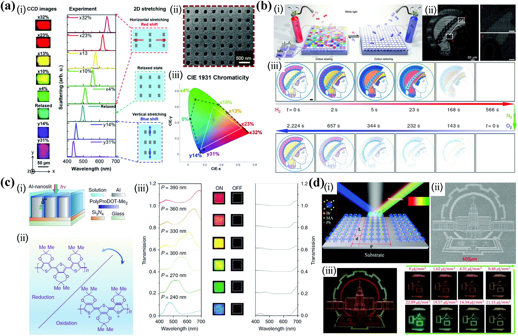 | ||
| Fig. 4 Dynamically tunable structural colors (a(i)–(iii)) a(i) CCD images and measured scattering spectra of Al plasmonic array at different stretching conditions. a(ii) SEM image of the Al-coated Si template at relaxed state. a(iii) Full-color tuning in 1931 CIE chromaticity diagram with different stretching ratios. Reproduced from ref. 118, with permission from American Chemical Society, Copyright 2017. (b(i)–(iii)) b(i) Schematic diagram of plasmonic metasurface consisting of hydrogen-responsive Mg nanoblocks sandwiched between a Ti adhesion layer and Ti/Pd capping layers. The structural colors can be erased by hydrogen exposure and restored by oxygen exposure. b(ii) SEM images of the printing picture of Minerva logo. b(iii) Measured optical images by microscope during the process of hydrogenation and dehydrogenation to erasing and restoring colors, respectively. Reproduced from ref. 121, with permission from Nature Publishing Group, Copyright 2017. (c(i)–(iii)) c(i) Schematic of plasmonic electrochromic electrode composed of Al-nanoslit array. c(ii) Chemical structures of PolyProDOT-Me2 in the oxidized and reduced form. c(iii) Measured transmission spectra of PolyProDOT-Me2-coated Al-nanoslit metasurface for ON and OFF states of the polymer. Insets show corresponding color micrographs with increasing periods. Reproduced from ref. 129, with permission from Nature Publishing Group, Copyright 2016. (d(i)–(iii)) d(i) The schematic design of lead halide perovskite nanostructures color generation by mixing extrinsic structural color and intrinsic emission color. d(ii) Top-view SEM image of the logo. d(iii) Dynamic color printing by MAPbBr3 meta-grating at different pumping density. Reproduced from ref. 132, with permission from American Chemical Society, Copyright 2018. | ||
Chemical transition is another way to realize dynamic tuning of structural colors; namely, tuning resonance via changing components of nanostructures, where Mg material with superior plasmonic properties is a perfect choice in the visible wavelength.119,120 In the field of solid-state hydrogen storage, Mg is one of the most promising candidates, because up to 7.6 wt% of hydrogen gas can be absorbed.119 Therefore, metallic-state Mg and dielectric-state MgH2 are able to undergo chemical transition via the processes of hydrogenation and dehydrogenation, respectively. Based on this unique property of catalytic Mg, Fig. 4b shows a dynamic color filter comprising an Mg layer sandwiched between Ti/Pd capping layers and a Ti adhesion layer.121 Upon hydrogen exposure, Mg nanoparticles will go through a series of complicated chemical processes, and the fraction of metal Mg will gradually decrease, rendering a dynamic change from plasmonic colors to dielectric colors. Due to the fact that the Mie resonances of MgH2 nanoparticles are weak in the visible range, the colors can be erased after hydrogenation. More importantly, the erased process is reversible through dehydrogenation in the presence of oxygen (Fig. 4b(iii)). The flexible colors are promising to be used in dynamic color displays with functionalities of tunable colors, encryption and animations.
Besides physical and chemical tuning, electronic control is also a good way to tune colors due to ultra-thin, low-power-consuming and flexible merits.122,123 In electronic technology, the phase transition from the nematic to the isotropic state of liquid crystals (LC) can be used to tune resonance under an applied voltage.108,124,125 However, the high cost, lack of bistability and complicated fabrication of LC nanostructures still remain a challenge. Hence, several electrochromic materials, such as conducting polymers and transition metal oxides, have been utilized to dynamically tune colors.126–128 For instance, Fig. 4c illustrates full-color electrochromic switching by use of polyaniline (PANI) and poly(2,2-dimethyl-3,4-propylenedioxythiophene) (PolyProDOT-Me2), which can both be conformally and controllable electrodeposited on Al nanoslits.129 To further improve the purity of colors, an Si3N4 waveguide as a buffer layer is set underneath the Al nanoslits to narrow the linewidth of the spectra (Fig. 4c(i)). By applying different voltages, oxidized and reductive PolyProDOT-Me2 with changing refractive indices will be switched, as shown in Fig. 4c(i), which means switching colors can be realized at ON and OFF states by using different voltages. The electrochromic switching with fast speed and high-contrast colors has promising applications, ranging from catalysis to photovoltaics.
Finally, photon doping can be used to realize dynamically tunable in situ structural colors. In addition to the extrinsic structural colors generated from light–matter interaction, the intrinsic emission colors caused by photoluminescence (PL) of the active materials is introduced in the photon-doping method.130,131 As shown in the schematic presented in Fig. 4d, methylammonium lead halide perovskite (MAPbBr3, where MA = CH3NH3+) gratings are patterned on a glass substrate via a top-down process.132 MAPbBr3 material as a semiconductor possesses intrinsic emissions generated from the direct bandgap. The intensity of the intrinsic emission colors can be determined by the excitation; that is, the density of the pumping laser. Hence, mixing of the extrinsic structural colors and intrinsic emission colors leads to a new color. Based on Grassmann's law, changing the intensity of intrinsic colors by use of a pumping laser enables the in situ new color to be dynamically tuned. The dynamic tuning is reversible with decreasing pumping intensity. More significantly, the color-transition time is mainly determined by buildup, and ring down time of PL is of the order of nanoseconds, which is orders of magnitude faster than previous studies. The enlarged measured printing in Fig. 4d(iii) shows flexibly dynamic tuning from red to green by changing the intensity of pumping light.
4. Applications
As shown in the previous sections, static and dynamic structural colors have been widely realized in metasurfaces. Because of the ultra-thin, ultracompact, highly durable and environmentally benign properties of the nanostructures, the full-color filters with high saturation, high efficiency and high resolution are promising alternatives to replace conventional pigments in many practical applications. In the following section, displays, encryption and sensing applications based on structural colors are introduced.To date, high-end and advanced displays have attracted the most attention in the study of structural colors. In Fig. 5a, a dynamic plasmonic nanostructure based on Au/Ag nanodomes is integrated into a designed matrix display covering the entire visible range.133 The method of electrodeposition can be utilized to dynamically alter the thickness of Ag shells on Au nanodomes by applying a voltage, and rendering a continuous color change based on a reversible redox reaction of Ag. During the process of redox, the colors will gradually change with the time of the oxidation/reduction reaction, which is consistent with the cyclic voltammogram measurement. In the design of a biomimetic chameleon (Fig. 5b(ii)), the chameleon covered with plasmonic nanodomes is equipped with color sensors to sense the environment's color. And then the color information is automatically analyzed and delivered into the nanodomes so as to change the color of the chameleon accordingly. This implies that optical wearable devices are possible. In Fig. 5a(iii), rapid display with the responsive speed of a unit cell and static display, where the unit cells are operated by a line-by-line matrix-addressing technique, are respectively demonstrated, showing the potential of high-end displays and imaging applications.
 | ||
| Fig. 5 Practical applications of structural colors generated from metasurface. (a(i)–(iii)) a(i) Schematic of designed plasmonic cell composed of nanodomes with different Ag shell thickness. a(ii) Schematic diagram of the plastic chameleon covered with plasmonic cells. a(iii) Operational schematic and screenshots of fast display and static display, which consist of designed plasmonic cells. Reproduced from ref. 133, with permission from American Chemical Society, Copyright 2016. (b(i)–(ii)) b(i) Schematic of Kerker-conditioned cryptographic nanostructures composed of a-Si:H nanoblocks over silica substrate. Different information can be decoded in a predetermined polarization angle. b(ii) Measured optical images of the encrypted “RHOLAB” message which can be decoded by polarized light at specific angle. Reproduced from ref. 134, with permission from Wiley-VCH Verlag GmbH & Co. KGaA, Weinheim, Copyright 2018. (c(i)–(v)) c(i) SEM image and c(ii) Schematic diagram of nanopin-cavity resonator for quantitative colorimetric ricin sensing. c(iii) Schematic of antibody immobilization on nanopins metasurface for ricin visual detection. c(iv) Bright-field micrograph of microfluidic channel device. Insets show enlarged SEM image of nanopins array and their color appearance. c(v) Spectra shift and colors variation of biofunctionalized procedure due to the inter-molecular interaction. Reproduced from ref. 139, with permission from Wiley-VCH Verlag GmbH & Co. KGaA, Weinheim, Copyright 2016. | ||
Fig. 5b shows a dynamic cryptographic nanostructure based on asymmetric a-Si:H nanoantennas on a silica substrate.134 By means of meticulously designing geometric parameters, Kerker's conditions can be fully met, and lead to a narrowed resonant peak and suppression of unwanted light; that is, improved saturation of structural colors. More importantly, the polarization-dependent property resulting from the asymmetric structures gives rise to the possibility of storing different optical information in distinct polarization states. As presented in Fig. 5b(i), a fixed nanostructure shows different quickmark codes in 0° and 90° polarization angles. Hence, the nanostructure can be a possible design strategy to realize cryptographic nanoprints via controlling polarization angles, such as the test of cryptograph shown in Fig. 5b(ii). Four kinds of pixel with 0° and 90° rotated angles for “R, O, A” and 45° and 135° rotated angles for “H, L, B” are used to encrypt information in designated polarization angles. These cryptographic nanoprints can be compatible with a smartphone, security tag, payment, identification and anti-counterfeiting.
Moreover, colorimetric sensing based on plasmonic structural colors has been introduced to detect analytes by directly observing changes of visible colors.42,135–138 However, the broad resonant spectra caused by localized surface plasmon resonance (LSPR) generally leads to reduced colorimetric resolution due to the strong radiative damping. For example, the highest LSPR sensitivity of an Au sensor is focused on the near-infrared range. To overcome the limitation of LSPR sensing, a skillfully designed strategy is used to improve colorimetric capacity. For instance, 2D Al nanoclusters have been designed to provide Fano resonance with energies in the region from blue to green, which is the most sensitive part for human eyes.138 The detected colors can gradually change from blue to orange when the analytes are air (n = 1.0), PDMS (n = 1.4), poly(methyl methacrylate) (PMMA) (n = 1.5) and diphenyl ether (n = 1.6), respectively. Furthermore, in the field of biosensing, quantitative colorimetric sensing of ricin is also reached in Fig. 5c based on nanopin-cavity resonator,139 by which bright-field structural colors are fully realized (Fig. 5c(ii)). The location of the resonant peak in the visible range can be flexibly tuned by changing the medium indices. As presented in Fig. 5c(iii), an antibody-functionalized biosensor with high sensitivity and fast response is fabricated to detect ricin. The antibody protein can be immobilized by use of the amide linkage formed by the reaction of the terminal succinimide group with the amine of protein. Based on the biosensor, the density of ricin can be observed by a dramatic color change at less than 10 min.
5. Summary and prospects
We have reviewed the development of structural colors based on plasmonic and dielectric metasurfaces to date. The plasmonic additive and subtractive colors caused by SPP resonance have been widely realized via nanogratings, nanoholes, disk-hole coupling and MIM nanostructures in both transmission and reflection modes. Although the inherent loss of metal materials hinders higher saturation and efficiency, remarkably high resolution approaching 100000 dpi is possible by use of disk-hole coupling. While for dielectric colors, Mie resonances generated from high-index dielectric nanostructures lead to high-quality reflection spectra with narrow linewidth and high efficiency; namely highly saturated colors. Significantly, a multi-dielectric metasurface based on multipolar modulation has recently obtained a huge color space occupied 171% sRGB space. However, there is still the challenge of realizing additive colors in the transmission mode within all-dielectric metasurfaces. Based on these color filters, a number of methods of dynamically tunable colors, including mechanical stretching, chemical reaction, electrical control and photon doping, are systematically discussed in this paper. The ultra-thin thickness of the color filters has the potential to integrate on a chip, indicating that structural colors generated from metasurfaces are promising in terms of a new paradigm for practical applications; for example, biosensing, colorimetric sensing, high-end displays, encryption, anti-counterfeiting, high-density optical data storage, holograms and so on. In summary, there is great significance and enormous potential application in the study of structural colors.
However, looking ahead, there are still obstacles that need to be addressed in the development of practical color filters. First of all, high-quality additive colors with both high saturation and high resolution are rare in the transmission mode, which is of significant importance for holograms and advanced imaging applications. In addition, color filters need to be combined with practical applications as much as possible. Mass production is still a challenge since Ag and Au are too expensive within plasmonic nanostructures, and TiO2 and c-Si are not compatible with CMOS process within dielectric nanostructures. Although Al or a-Si seem to be good choices for practical production, high loss invariably hampers the generation of highly saturated colors. That means new designed strategies and fabricated technologies are imminently required in the subsequent research. For instance, hybridization between dielectric and plasmonic materials can be a promising platform for additive structural colors in the transmission mode by meticulous design. On the other hand, possible approaches in terms of nanoimprint lithography, self-assembly technique and injection molding need to be developed in practice to realize mass production. Overall, there is still huge space to be explored in relation to structural colors before commercialization. We believe colors generated from metasurfaces can be extensively used to take the place of chemical pigments, and dramatically improve the quality of our daily life in the future.
Conflicts of interest
There are no conflicts to declare.Acknowledgements
This work was supported by the National Key Research and Development Program of China (2016YFA0301102 and 2017YFA0303800), the National Natural Science Foundation of China (91856101, 11574163, and 11774186), Natural Science Foundation of Tianjin for Distinguished Young Scientists (18JCJQJC45700), the Natural Science Foundation of Tianjin (16JCQNJC01700), and 111 Project (B07013).Notes and references
- O. Meth-Cohn and M. Smith, J. Chem. Soc., Perkin Trans. 1, 1994, 5–7 RSC.
- D. D. Oprian, A. B. Asenjo, N. Lee and S. L. Pelletier, Biochemistry, 1991, 30, 11367–11372 CrossRef CAS PubMed.
- A. J. Melendez-Martinez, G. Britton, I. M. Vicario and F. J. Heredia, Food Chem., 2007, 101, 1145–1150 CrossRef CAS.
- Z. Hao and A. Iqbal, Chem. Soc. Rev., 1997, 26, 203–213 RSC.
- W. Yue, S. Gao, S.-S. Lee, E.-S. Kim and D.-Y. Choi, Laser Photonics Rev., 2017, 11, 1600285 CrossRef.
- Y. Wang, M. Zheng, Q. Ruan, Y. Zhou, Y. Chen, P. Dai, Z. Yang, Z. Lin, Y. Long, Y. Li, N. Liu, C.-W. Qiu, J. K. W. Yang and H. Duan, Research, 2018, 8109054 Search PubMed.
- H. Ghiradella, Appl. Opt., 1991, 30, 3492–3500 CrossRef CAS PubMed.
- S. Kinoshita, S. Yoshioka and J. Miyazaki, Rep. Prog. Phys., 2008, 71, 076401 CrossRef.
- Y. Fu, C. A. Tippets, E. U. Donev and R. Lopez, Wiley Interdiscip. Rev.: Nanomed. Nanobiotechnol., 2016, 8, 758–775 Search PubMed.
- K. Zhang, Y. Tang, J. Meng, G. Wang, H. Zhou, T. Fan and D. Zhang, Opt. Express, 2014, 22, 27437–27450 CrossRef PubMed.
- N. Okada, D. Zhu, D. Cai, J. B. Cole, M. Kambe and S. Kinoshita, J. Opt., 2013, 42, 25–36 CrossRef.
- Y. Shen, V. Rinnerbauer, I. Wang, V. Stelmakh, J. D. Joannopoulos and M. Soljacic, ACS Photonics, 2015, 2, 27–32 CrossRef CAS.
- F. Cheng, J. Gao, T. S. Luk and X. Yang, Sci. Rep., 2015, 5, 11045 CrossRef CAS PubMed.
- J. S. Clausen, E. Højlund-Nielsen, A. B. Christiansen, S. Yazdi, M. Grajower, H. Taha, U. Levy, A. Kristensen and N. A. Mortensen, Nano Lett., 2014, 14, 4499–4504 CrossRef CAS PubMed.
- T. Xu, H. Shi, Y.-K. Wu, A. F. Kaplan, J. G. Ok and L. J. Guo, Small, 2011, 7, 3128–3136 CrossRef CAS PubMed.
- Y. Gu, L. Zhang, J. K. W. Yang, S. P. Yeo and C.-W. Qiu, Nanoscale, 2015, 7, 6409 RSC.
- P. Genevet, F. Capasso, F. Aieta, M. Khorasaninejad and R. Devlin, Optica, 2017, 4, 139–152 CrossRef CAS.
- E. Karimi, S. A. Schulz, I. D. Leon, H. Qassim, J. Upham and R. W. Boyd, Light: Sci. Appl., 2014, 3, e167 CrossRef CAS.
- N. Meinzer, W. L. Barnes and L. R. Hooper, Nat. Photonics, 2014, 8, 889 CrossRef CAS.
- J. Wang and J. Du, Appl. Sci., 2016, 6, 239 CrossRef.
- A. Krasnok, S. Makarov, M. Petrov, R. Savelev, P. Belov and Y. Kivshar, SPIE Opt. Optoelectr., 2015, 9502, 950203 Search PubMed.
- M. I. Shalaev, J. Sun, A. Tsukernik, A. Pandey, K. Nikolskiy and N. M. Litchinitser, Nano Lett., 2015, 15, 6261–6266 CrossRef CAS PubMed.
- A. I. Kuznetsov, A. E. Miroshnichenko, M. L. Brongersma, Y. S. Kivshar and B. Luk’yanchuk, Science, 2016, 354, aag2472 CrossRef PubMed.
- X. Yin, Z. Ye, J. Rho, Y. Wang and X. Zhang, Science, 2013, 339, 1405–1407 CrossRef CAS.
- Z. Li, W. Liu, H. Cheng, S. Chen and J. Tian, Adv. Opt. Mater., 2017, 5, 1700413 CrossRef.
- Z. Li, W. Liu, H. Cheng, J. Liu, S. Chen and J. Tian, Sci. Rep., 2016, 6, 35485 CrossRef CAS PubMed.
- Z. Li, W. Liu, H. Cheng, S. Chen and J. Tian, Opt. Lett., 2016, 41, 3142–3145 CrossRef CAS PubMed.
- J. Lee, M. Tymchenko, C. Argyropoulos, P.-Y. Chen, F. Lu, F. Demmerle, G. Boehm, M.-C. Amann, A. Alù and M. A. Belkin, Nature, 2014, 511, 65 CrossRef CAS PubMed.
- Z. Li, W. Liu, Z. Li, H. Cheng, S. Chen and J. Tian, Opt. Lett., 2017, 42, 3117–3120 CrossRef CAS PubMed.
- Z. Li, W. Liu, Z. Li, H. Cheng, J. Li, X. Chen, S. Chen and J. Tian, Laser Photonics Rev., 2018, 12, 1800164 CrossRef.
- A. V. Kildishev, A. Boltasseva and V. M. Shalaev, Science, 2013, 339, 1232009 CrossRef PubMed.
- L. Huang, X. Chen, B. Bai, Q. Tan, G. Jin, T. Zentgraf and S. Zhang, Light: Sci. Appl., 2013, 2, e70 CrossRef.
- S. Chen, Z. Li, W. Liu, H. Cheng and J. Tian, Adv. Mater., 2019, 1802458 CrossRef PubMed.
- L. Huang, X. Chen, H. Mühlenbernd, H. Zhang, S. Chen, B. Bai, Q. Tan, G. Jin, K.-W. Cheah, C.-W. Qiu, J. Li, T. Zentgraf and S. Zhang, Nat. Commun., 2013, 4, 2808 CrossRef.
- G. Zheng, H. Mühlenbernd, M. Kenney, G. Li, T. Zentgraf and S. Zhang, Nat. Nanotechnol., 2015, 10, 308 CrossRef CAS PubMed.
- Z. Li, M.-H. Kim, C. Wang, Z. Han, S. Shrestha, A. C. Overvig, M. Lu, A. Stein, A. M. Agarwal, M. Lončar and N. Yu, Nat. Nanotechnol., 2017, 12, 675 CrossRef CAS PubMed.
- A. Pors, M. G. Nielsen, R. L. Eriksen and S. I. Bozhevolnyi, Nano Lett., 2013, 13, 829–834 CrossRef CAS PubMed.
- A. A. High, R. C. Devlin, A. Dibos, M. Polking, D. S. Wild, J. Perczel, N. P. de Leon, M. D. Lukin and H. Park, Nature, 2015, 522, 192 CrossRef CAS PubMed.
- N. Yu, F. Aieta, P. Genevet, M. A. Kats, Z. Gaburro and F. Capasso, Nano Lett., 2012, 12, 6328–6333 CrossRef CAS PubMed.
- F. Ding, Z. Wang, S. He, V. M. Shalaev and A. V. Kildishev, ACS Nano, 2015, 9, 4111–4119 CrossRef CAS PubMed.
- Z. Li, A. W. Clark and J. M. Cooper, ACS Nano, 2016, 10, 492–498 CrossRef CAS PubMed.
- M. Song, X. Li, M. Pu, Y. Guo, K. Liu, H. Yu, X. Ma and X. Luo, Nanophotonics, 2018, 7, 323–331 Search PubMed.
- L. Duempelmann, A. Luu-Dinh, B. Gallinet and L. Novotny, ACS Photonics, 2016, 3, 190–196 CrossRef CAS.
- X. M. Goh, Y. Zheng, S. J. Tan, L. Zhang, K. Kumar, C.-W. Qiu and J. K. W. Yang, Nat. Commun., 2014, 5, 5361 CrossRef CAS PubMed.
- J.-M. Guay, A. C. Lesina, G. Côté, M. Charron, D. Poitras, L. Ramunno, P. Berini and A. Weck, Nat. Commun., 2017, 8, 16095 CrossRef CAS PubMed.
- Q. Chen and D. R. S. Cumming, Opt. Express, 2010, 18, 14056–14062 CrossRef CAS PubMed.
- F. Cheng, J. Gao, L. Stan, D. Rosenmann, D. Czaplewski and X. Yang, Opt. Express, 2015, 23, 14552–14560 CrossRef CAS PubMed.
- F. Cheng, X. Yang, D. Rosenmann, L. Stan, D. Czaplewski and J. Gao, Opt. Express, 2015, 23, 25329–25339 CrossRef CAS PubMed.
- W. Wang, D. Rosenmann, D. A. Czaplewski, X. Yang and J. Gao, Opt. Express, 2017, 25, 20454–20465 CrossRef CAS PubMed.
- Z. Wei, Y. Cao, X. Su, Z. Gong, Y. Long and H. Li, Opt. Express, 2013, 21, 10739–10745 CrossRef PubMed.
- B. Zeng, Y. Gao and F. J. Bartoil, Sci. Rep., 2013, 3, 2840 CrossRef PubMed.
- T. Xu, Y.-K. Wu, X. Luo and L. J. Guo, Nat. Commun., 2010, 1, 59 Search PubMed.
- H. J. Park, T. Xu, J. Y. Lee, A. Ledbetter and L. J. Guo, ACS Nano, 2011, 5, 7055–7060 CrossRef CAS PubMed.
- H.-S. Lee, Y.-T. Yoon, S.-S. Lee, S.-H. Kim and K.-D. Lee, Opt. Express, 2007, 15, 15457–15463 CrossRef PubMed.
- D. Inoue, A. Miura, T. Nomura, H. Fujikawa, K. Sato, N. Ikeda, D. Tsuya, Y. Sugimoto and Y. Koide, Appl. Phys. Lett., 2011, 98, 093113 CrossRef.
- M. Miyata, H. Hatada and J. Takahara, Nano Lett., 2016, 16, 3166–3172 CrossRef CAS.
- H. Kim, M. Kim, T. Chang, A. Baucour, S. Jeon, N. Kim, H.-J. Choi, H. Lee and J. Shin, Opt. Express, 2018, 26, 27403–27417 CrossRef.
- A. S. Roberts, A. P. Albreksten and S. I. Bozhevolnyi, Nano Lett., 2014, 14, 783–787 CrossRef CAS PubMed.
- C. Yang, W. Shen, Y. Zhang, H. Peng, X. Zhang and X. Liu, Opt. Express, 2014, 22, 11384–11391 CrossRef PubMed.
- Y. Ren, Y. Lu, T. Zang, Y. Wang, Y. Dai and P. Wang, Opt. Express, 2017, 25, 28417–28426 CrossRef CAS.
- H. Wang, X. Wang, C. Yan, H. Zhao, J. Zhang, C. Santschi and O. J. F. Martin, ACS Nano, 2017, 11, 4419–4427 CrossRef CAS PubMed.
- S. J. Tan, L. Zhang, D. Zhu, X. M. Goh, Y. M. Wang, K. Kumar, C.-W. Qiu and J. K. W. Yang, Nano Lett., 2014, 14, 4023–4029 CrossRef CAS PubMed.
- J. S. Clausen, E. Højlund-Nielsen, A. B. Christiansen, S. Yazdi, M. Grajower, H. Taha, U. Levy, A. Kristensen and N. A. Mortensen, Nano Lett., 2014, 14, 4499–4504 CrossRef CAS PubMed.
- X. Zhu, C. Vannahme, E. Højlund-Nielsen, N. A. Mortensen and A. Kristensen, Nat. Nanotechnol., 2016, 11, 325–329 CrossRef CAS PubMed.
- B.-R. Lu, C. Xu, J. Liao, J. Liu and Y. Chen, Opt. Lett., 2016, 41, 1400–1403 CrossRef CAS PubMed.
- K. Kumar, H. Duan, R. S. Hegde, S. C. W. Koh, J. N. Wei and J. K. W. Yang, Nat. Nanotechnol., 2012, 7, 557 CrossRef CAS.
- P. Mandal, S. A. Ramakrishna, R. Patil and A. V. Gopal, Appl. Phys. Lett., 2013, 114, 224303 Search PubMed.
- A. G. Nikitin, Appl. Phys. Lett., 2016, 108, 051112 CrossRef.
- K.-T. Lee, S. Y. Han and H. J. Park, Adv. Opt. Mater., 2017, 5, 1700284 CrossRef.
- L. Wang, R. J. H. Ng, S. S. Dinachali, M. Jalali, Y. Yu and J. K. W. Yang, ACS Photonics, 2016, 3, 627–633 CrossRef CAS.
- R. Yu, P. Mazumder, N. F. Borrelli, A. Carrilero, D. S. Ghosh, R. A. Maniyara, D. Baker, F. J. G. de Abajo and V. Pruneri, ACS Photonics, 2016, 3, 1194–1201 CrossRef CAS.
- X. M. Goh, R. J. H. Ng, S. Wang, S. J. Tan and J. K. W. Yang, ACS Photonics, 2016, 3, 1000–1009 CrossRef CAS.
- R. J. H. Ng, X. M. Goh and J. K. W. Yang, Opt. Express, 2015, 23, 32597–32605 CrossRef CAS PubMed.
- Z. Li, W. Wang, D. Rosenmann, D. A. Czaplewski, X. Yang and J. Gao, Opt. Express, 2016, 24, 20472–20480 CrossRef CAS PubMed.
- M. Ye, L. Sun, X. Hu, B. Shi, B. Zeng, L. Wang, J. Zhao, S. Yang, R. Tai, H.-J. Fecht, J.-Z. Jiang and D.-X. Zhang, Opt. Lett., 2015, 40, 4979–4982 CrossRef CAS PubMed.
- Z. Li, S. Butun and K. Aydin, ACS Photonics, 2015, 2, 183–188 CrossRef CAS.
- Y.-K. R. Wu, A. E. Hollowell, C. Zhang and L. J. Guo, Sci. Rep., 2013, 3, 1194 CrossRef PubMed.
- J. Olson, A. Manjavacas, L. Liu, W.-S. Chang, B. Foerster, N. S. King, M. W. Knight, P. Nordlander, N. J. Halas and S. Link, Proc. Natl. Acad. Sci. U. S. A., 2014, 111, 14348–14353 CrossRef CAS PubMed.
- S. Jahani and Z. Jacob, Nat. Nanotechnol., 2016, 11, 23 CrossRef CAS PubMed.
- Z. Ma, S. M. Hanham, P. Albella, B. Ng, H. T. Lu, Y. Gong, S. A. Maier and M. Hong, ACS Photonics, 2016, 3, 1010–1018 CrossRef CAS.
- M. Decker, I. Staude, M. Falkner, J. Dominguez, D. N. Neshev, I. Brener, T. Pertsch and Y. S. Kivshar, Adv. Opt. Mater., 2015, 3, 813–820 CrossRef CAS.
- C. Wu, N. Arju, G. Kelp, J. A. Fan, J. Dominguez, E. Gonzales, E. Tutuc, I. Brener and G. Shvets, Nat. Commun., 2014, 5, 3892 CrossRef CAS PubMed.
- K. E. Chong, I. Staude, A. James, J. Dominguez, S. Liu, S. Campione, G. S. Subramania, T. S. Luk, M. Decker, D. N. Neshev, I. Brener and Y. S. Kivshar, Nano Lett., 2015, 15, 5369–5374 CrossRef CAS PubMed.
- D. Sell, J. Yang, S. Doshay, K. Zhang and J. A. Fan, ACS Photonics, 2016, 3, 1919–1925 CrossRef CAS.
- V. Vashistha, G. Vaidya, R. S. Hegde, A. F. Serebryannikov, N. Bonod and M. Krawczyk, ACS Photonics, 2017, 4, 1076–1082 CrossRef CAS.
- Z. Dong, J. Ho, Y. F. Yu, Y. H. Fu, R. Paniagua-Dominguez, S. Wang, A. I. Kuznetsov and J. K. W. Yang, Nano Lett., 2017, 17, 7620–7628 CrossRef CAS PubMed.
- R. Alaee, R. Filter, D. Lehr, F. Lederer and C. Rockstuhl, Opt. Lett., 2015, 40, 2645–2648 CrossRef CAS PubMed.
- V. E. Babicheva and A. B. Evlyukhin, Laser Photonics Rev., 2017, 11, 1700132 CrossRef.
- S. V. Makarov, A. N. Tsypkin, T. A. Voytova, V. A. Milichko, I. S. Mukhin, A. V. Yulin, S. E. Putilin, M. A. Baranov, A. E. Krasnok, I. A. Morozov and P. A. Belov, Nanoscale, 2016, 8, 17809–17814 RSC.
- I. Koirala, V. R. Shrestha, C.-S. Park, S. Gao, S.-S. Lee and D.-Y. Choi, Sci. Rep., 2017, 7, 2556 CrossRef PubMed.
- C.-S. Park, V. R. Shrestha, W. Yue, S. Gao, S.-S. Lee, E.-S. Kim and D.-Y. Choi, Sci. Rep., 2017, 7, 2556 CrossRef PubMed.
- E. D. Palik, Handbook of optical constants of solids, Academic Press, New York, 1991 Search PubMed.
- Z. Zhou, J. Li, R. Su, B. Yao, H. Fang, K. Li, L. Zhou, J. Liu, D. Stellinga, C. P. Reardon, T. F. Krauss and X. Wang, ACS Photonics, 2017, 4, 544–551 CrossRef CAS.
- Y. Nagasaki, M. Suzuki and J. Takahara, Nano Lett., 2017, 17, 7500–7506 CrossRef CAS PubMed.
- J. P. B. Mueller, N. A. Rubin, R. C. Devlin, B. Groever and F. Capasso, Phys. Rev. Lett., 2017, 118, 113901 CrossRef PubMed.
- M. Khorasaninejad, Z. Shi, A. Y. Zhu, W. T. Chen, V. Sanjeev, A. Zaidi and F. Capasso, Nano Lett., 2017, 17, 1819–1824 CrossRef CAS PubMed.
- S. Sun, Z. Zhou, C. Zhang, Y. Gao, Z. Duan, S. Xiao and Q. Song, ACS Nano, 2017, 11, 4445–4452 CrossRef CAS PubMed.
- B. Yang, W. Liu, Z. Li, H. Cheng, S. Chen and J. Tian, Adv. Opt. Mater., 2018, 6, 1701009 CrossRef.
- M. J. Uddin, T. Khaleque and R. Magnusson, Opt. Express, 2014, 22, 12307–12315 CrossRef CAS PubMed.
- M. J. Uddin and R. Magnusson, Opt. Express, 2013, 21, 12495–12506 CrossRef PubMed.
- W. Zhang, M. Anaya, G. Lozano, M. E. Calvo, M. B. Johnston, H. Míguez and H. J. Snaith, Nano Lett., 2015, 15, 1698–1702 CrossRef CAS PubMed.
- B. Gholipour, G. Adamo, D. Cortecchia, H. N. S. Krishnamoorthy, M. D. Birowosuto, N. I. Zheludev and C. Soci, Adv. Mater., 2017, 29, 1604268 CrossRef PubMed.
- T. Wood, M. Naffouti, J. Berthelot, T. David, J.-B. Claude, L. Métayer, A. Delobbe, L. Favre, A. Ronda, I. Berbezier, N. Bonod and M. Abbarchi, ACS Photonics, 2017, 4, 873–883 CrossRef CAS.
- X. Zhu, W. Yan, U. Levy, N. A. Mortensen and A. Kristensen, Sci. Adv., 2017, 3, e1602487 CrossRef.
- B. Yang, W. Liu, Z. Li, H. Cheng, D.-Y. Choi, S. Chen and J. Tian, Nano Lett., 2019 DOI:10.1021/acs.nanolett.8b04923.
- V.-C. Su, C. H. Chu, G. Sun and D. P. Tsai, Opt. Express, 2018, 26, 13148–13182 CrossRef CAS PubMed.
- H.-T. Chen, A. J. Taylor and N. Yu, Rep. Prog. Phys., 2016, 79, 076401 CrossRef PubMed.
- J. Sautter, I. Staude, M. Decker, E. Rusak, D. N. Neshev, I. Brener and Y. S. Kivshar, ACS Nano, 2015, 9, 4308–4315 CrossRef CAS.
- P. Gutruf, C. Zou, W. Withayachumnankul, M. Bhaskaran, S. Sriram and C. Fumeaux, ACS Nano, 2015, 10, 133–141 CrossRef.
- H. Cheng, S. Chen, P. Yu, W. Liu, Z. Li, J. Li, B. Xie and J. Tian, Adv. Opt. Mater., 2015, 3, 1744–1749 CrossRef CAS.
- M. Seo, J. Kyoung, H. Park, S. Koo, H.-S. Kim, H. Bernien, B. J. Kim, J. H. Choe, Y. H. Ahn, H.-T. Kim, N. Park, Q.-H. Park, K. Ahn and D.-S. Kim, Nano Lett., 2010, 10, 2064–2068 CrossRef CAS PubMed.
- J. Y. Ou, E. Plum, L. Jiang and N. I. Zheludev, Nano Lett., 2011, 11, 2142–2144 CrossRef CAS PubMed.
- A. Benz, I. Montano, J. F. Klem and I. Brener, Appl. Phys. Lett., 2013, 103, 263116 CrossRef.
- I. M. Pryce, K. Aydin, Y. A. Kelaita, R. M. Briggs and H. A. Atwater, Nano Lett., 2010, 10, 4222–4227 CrossRef CAS PubMed.
- S.-I. Park, Y. Xiong, R.-H. Kim, P. Elvikis, M. Meitl, D.-H. Kim, J. Wu, J. Yoon, C.-J. Yu, Z. Liu, Y. Huang, K. Hwang, P. Ferreira, X. Li, K. Choquette and J. A. Rogers, Science, 2009, 325, 977–981 CrossRef CAS PubMed.
- Y. Yao, R. Shankar, M. A. Kats, Y. Song, J. Kong, M. Loncar and F. Capasso, Nano Lett., 2014, 14, 6526–6532 CrossRef CAS PubMed.
- H.-S. Ee and R. Agarwal, Nano Lett., 2016, 16, 2818–2823 CrossRef CAS PubMed.
- M. L. Tseng, J. Yang, M. Semmlinger, C. Zhang, P. Nordlander and N. J. Halas, Nano Lett., 2017, 17, 6034–6039 CrossRef CAS PubMed.
- F. Sterl, N. Strohfeldt, R. Walter, R. Griessen, A. Tittl and H. Giessen, Nano Lett., 2015, 15, 7949–7955 CrossRef CAS PubMed.
- Y. Chen, X. Duan, M. Matuschek, Y. Zhou, F. Neubrech, H. Duan and N. Liu, Nano Lett., 2017, 17, 5555–5560 CrossRef CAS PubMed.
- X. Duan, S. Kamin and N. Liu, Nat. Commun., 2017, 8, 14606 CrossRef CAS PubMed.
- S. N. Burokur, J.-P. Daniel, P. Ratajczak and A. de Lustrac, Appl. Phys. Lett., 2010, 97, 064101 CrossRef.
- Y. Lee, M.-K. Park, S. Kim, J. H. Shin, C. Moon, J. Y. Hwang, J.-C. Choi, H. Park, H.-R. Kim and J. E. Jang, ACS Photonics, 2017, 4, 1954–1966 CrossRef CAS.
- M. Decker, C. Kremers, A. Minovich, I. Staude, A. E. Miroshnichenko, D. Chigrin, D. N. Neshev, C. Jagadish and Y. S. Kivshar, Opt. Express, 2013, 21, 8879–8885 CrossRef PubMed.
- O. Buchnev, N. Podoliak, M. Kaczmarek, N. I. Zheludev and V. A. Fedotov, Adv. Opt. Mater., 2015, 3, 674–679 CrossRef CAS.
- S. K. Deb and J. A. Chopoorian, J. Appl. Phys., 1966, 37, 4818–4825 CrossRef CAS.
- D. R. Rosseinsky and R. J. Mortimer, Adv. Mater., 2011, 13, 783–793 CrossRef.
- A. A. Argun, P.-H. Aubert, B. C. Thompson, I. Schwendeman, C. L. Gaupp, J. Hwang, N. J. Pinto, D. B. Tanner, A. G. MacDiarmid and J. R. Reynolds, Chem. Mater., 2004, 16, 4401–4412 CrossRef CAS.
- T. Xu, E. C. Walter, A. Agrawal, C. Bohn, J. Velmurugan, W. Zhu, H. J. Lezec and A. A. Talin, Nat. Commun., 2016, 7, 10479 CrossRef CAS.
- S. D. Stranks and H. J. Snaith, Nat. Nanotechnol., 2015, 10, 391 CrossRef CAS PubMed.
- B. R. Sutherland and E. H. Sargent, Nat. Photonics, 2016, 10, 295 CrossRef CAS.
- Y. Gao, C. Huang, C. Hao, S. Sun, L. Zhang, C. Zhang, Z. Duan, K. Wang, Z. Jin, N. Zhang, A. V. Kildishev, C.-W. Qiu, Q. Song and S. Xiao, ACS Nano, 2018, 12, 8847–8854 CrossRef CAS PubMed.
- G. Wang, X. Chen, S. Liu, C. Wong and S. Chu, ACS Nano, 2016, 10, 1788–1794 CrossRef CAS PubMed.
- J. Jang, H. Jeong, G. Hu, C.-W. Qiu, K. T. Nam and J. Rho, Adv. Opt. Mater., 2018, 1801070 CrossRef.
- S. Sun, W. Yang, C. Zhang, J. Jing, Y. Gao, X. Yu, Q. Song and S. Xiao, ACS Nano, 2018, 12, 2151–2159 CrossRef CAS.
- J. Proust, F. Bedu, B. Gallas, I. Ozerov and N. Bonod, ACS Nano, 2016, 10, 7761–7767 CrossRef CAS.
- R. Verre, N. Maccaferri, K. Fleischer, M. Svedendahl, N. O. Länk, A. Dmitriev, P. Vavassori, I. V. Shvets and M. Käll, Nanoscale, 2016, 8, 10576–10581 RSC.
- N. S. King, L. Liu, X. Yang, B. Cerjan, H. O. Everitt, P. Nordlander and N. J. Halas, ACS Nano, 2015, 9, 10628–10636 CrossRef CAS PubMed.
- R. Fan, J. Zhu, W.-G. Wu and Y. Huang, Small, 2017, 13, 1601710 CrossRef PubMed.
| This journal is © the Partner Organisations 2019 |