
 Open Access Article
 This Open Access Article is licensed under a Creative Commons Attribution-Non Commercial 3.0 Unported Licence
Polarized Raman spectroscopy to elucidate the texture of synthesized MoS2†
Vincent
Vandalon
 *a,
Akhil
Sharma
a,
Alberto
Perrotta
b,
Benedikt
Schrode
b,
Marcel A.
Verheijen
ac and
Ageeth A.
Bol
*a
*a,
Akhil
Sharma
a,
Alberto
Perrotta
b,
Benedikt
Schrode
b,
Marcel A.
Verheijen
ac and
Ageeth A.
Bol
*a
aApplied Physics, Eindhoven University of Technology, 5600MB Eindhoven, The Netherlands. E-mail: v.vandalon@tue.nl; a.a.bol@tue.nl
bInstitute of Solid State Physics, Graz University of Technology, 8010 Graz, Austria
cEurofins Material Science Netherlands BV, 5656AE Eindhoven, The Netherlands
First published on 15th November 2019
Abstract
Texture has a significant impact on several key properties of transition-metal dichalcogenides (TMDs) films. Films with in-plane oriented grains have been successfully implemented in nano- and opto-electronic devices, whereas, films with out-of-plane oriented material have shown excellent performance in catalytic applications. It will be demonstrated that the texture of nanocrystalline TMD films can be determined with polarized Raman spectroscopy. A model describing the impact of texture on the Raman response of 2D-TMDs will be presented. For the specific case of MoS2, the model was used to quantify the impact of texture on the relative strength of the A1g and E12g modes in both the unpolarized and polarized Raman configuration. Subsequently, the capability to characterize texture by polarized Raman was demonstrated on various MoS2 films grown by atomic-layer deposition (ALD) and validated by complementary transmission electron microscopy (TEM) and synchrotron based 2D grazing-incidence X-ray diffraction (GIXD) measurements. This also revealed how the texture evolved during ALD growth of MoS2 and subsequent annealing of the films. The insights presented in this work allow a deeper understanding of Raman spectra of nanocrystalline TMDs and enable a rapid and non-destructive method to probe texture.
Introduction
Layered 2D transition-metal dichalcogenides (TMDs) are a class of promising materials with applications in the fields of catalysis, photonics, opto- and nano-electronics.1–8 Excellent transistor characteristics and logic performance have already been demonstrated for mono and few layered TMDs obtained by exfoliation and outstanding catalytic performance has also been shown for TMD films.4,9–13 However, in order to adopt these materials in the field of nanoelectronics, the development of scalable synthesis methods for 2D TMDs such as MoS2 and WS2 are essential.14–17 This is closely intertwined with the development of reliable characterization techniques for synthesized TMDs, in which Raman spectroscopy is of particular interest. Raman spectroscopy has already emerged as the go-to technique for characterization of exfoliated single-crystalline TMDs yielding insight into e.g. crystallinity and layer thickness.18–21 In contrast to the large single-crystalline flakes, the synthesized material is typically nanocrystalline in nature with grain size ranging from at best a few hundred nanometres down to tens of nanometres.15,16,22,23 Larger grain sizes have so far only be obtained with greatly reduced growth rates or with specially optimized workflows not compatible with large-area synthesis.24–26 Furthermore, synthesized TMDs exhibit a wide range of textures depending on the synthesis conditions as reported for e.g. atomic-layer deposition (ALD) and chemical vapour deposition (CVD).12,15,17,27–31 Synthetic MoS2 films can be amorphous or crystalline with a texture of the crystalline material ranging from in-plane oriented grains (i.e. horizontally aligned layers) to complex 3D structures with out-of-plane oriented (OoPO) grains (i.e. edge-on fins).15,17,27 It is well known that the differences in grain orientation of these highly anisotropic materials significantly impact film properties.2,27,31–33 Horizontally aligned grains are typically well suited for electronic applications, while OoPO grains are very efficient electrocatalysts. It is therefore of paramount importance to be able to characterize the texture of synthesized TMDs to optimize performance. Furthermore, insight into the evolution of the texture during synthesis can yield a deeper understanding of the underlying growth mechanism and crystallization kinetics, aiding in the further optimization of film properties for the specific applications.To obtain insight into the texture of the TMD films, both the local structure of the grains (e.g. shape, size) and the average grain orientation are of interest. A convenient metric for the average grain orientation is the angular grain distribution also known as the orientation distribution function (ODF) in X-ray crystallography.34 The angular grain distribution describes the volume fraction of grains as a function of the orientation of their crystal axes. In practice, the orientation of a TMD crystal can be described by the angle between the c axis (as defined in Fig. 1(a)) and the surface normal; in most cases the a axis is oriented randomly due to the van der Waals nature of the TMDs. Of the established diagnostic techniques, high-resolution transmission electron microscopy (HR-TEM) is excellently suited to investigate the local structure but typically lacks the field-of-view to efficiently gather enough data to gain insight into the angular grain distribution. Moreover, sample preparation for the especially insightful cross-section HR-TEM analysis is destructive and time consuming. X-ray diffraction (XRD) does yield (limited) quantitative insight into the angular grain orientation but only in rare cases is it feasible to determine the full angular grain distribution; in general only the texture coefficients are determined which only gives qualitative information.34 Furthermore, the XRD signal from mono- and few-layer TMDs is typically too weak to obtain quantitative information related to the texture. In practice, often only a few selected samples are analysed out of a larger series due to the relatively low throughput of HR-TEM and XRD. This clearly outlines the need for a non-destructive, ubiquitous, and rapid methodology that is capable of determining the angular grain distribution of these TMDs.
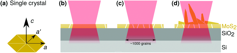 | ||
| Fig. 1 (a) Definitions of the crystal axis for the 2D TMDs such as MoS2. (b) For TMDs obtained by exfoliation, the Raman response originates from a single grain because the spot size (pink area) ≪ grain size. Generally, the c-axis of the exfoliated material will be oriented parallel to the surface normal. (c & d) For synthesized material, the grain size is typically on the nanometre scale and therefore the Raman response has contributions from many grains. Depending on the synthesis conditions, the nanocrystalline material can show (c) a preferred orientation such as in-plane oriented grains or (d) more out-of-plane oriented grains in the form of fins. | ||
In this work, it will be demonstrated that polarized Raman spectroscopy is excellently suited for determining the angular grain distribution of (nano-) crystalline TMDs possessing the D3h/D6h point group such as 2H-MoS2 or 2H-WS2. The Raman response of these materials is dominated by the out-of-plane A1g and the in-plane E12g vibrations although weaker and defect related contributions are also present.35–37 For these TMDs, the non-polarized variant of Raman spectroscopy is already an indispensable characterization method as stated before and it is used to probe crystallinity, crystal quality, and gives a measure of film thickness.20,38,39 The indispensability is partly due to the sensitivity of Raman spectroscopy towards these properties, but also due to Raman spectroscopy being a contactless and non-destructive measurement requiring (virtually) no sample preparation. Therefore, the Raman response of TMDs has been studied extensively both theoretically and experimentally with the main focus so far on the understanding of the Raman response of (nearly ideal) single crystals.37,40,41 Conversely, a fundamental understanding of the Raman response of nanocrystalline TMDs – and especially insight into the impact of texture – is lacking. The need for more insight is illustrated by, for example, Kong et al. whom reported a ∼3 times higher A1g/E12g ratio for OoPO grains compared to in-plane oriented grains.12,42 They speculate that this is most likely caused by the differences in texture but they lacked a framework to fully interpret this result.12,42 Moreover, it is unclear if and how the Raman response can be used to obtain insight into the angular grain distribution of these nanocrystalline TMDs. Here, both topics are addressed: (1) the impact of the angular grain distribution on the Raman response will be modelled considering both the non-polarized and polarized variants of Raman spectroscopy. This will provide fundamental insight into the impact of the angular grain distribution on the Raman response. (2) This will also allow us to deduce that polarized Raman measurements can be used to determine the angular grain distribution. Our work will demonstrate that polarized Raman spectroscopy is a versatile, easy to use technique to study the texture of various 2D transition metal dichalcogenides.
The capability of polarized Raman spectroscopy to probe the angular grain distribution will be demonstrated on MoS2 films ranging in texture from OoPO edge-on sheets to nearly ideal horizontally oriented grains. The texture of MoS2 films, synthesized by either plasma-enhanced atomic-layer deposition (PE-ALD) or by thermal sulphurization of MoOx films, will be determined using polarized Raman spectroscopy. To validate the Raman based approach, complementary texture measurements using techniques including synchrotron based 2D grazing-incidence X-ray diffraction (GIXD) and cross-section TEM will be performed. Following the validation of the Raman analysis, the impact of a high-temperature anneal in H2S gas on the texture of the MoS2 films will be studied. This should reveal if the improved photoluminescence (PL) of the annealed films is (in part) correlated to a change in texture.
Results and discussion
Raman response of nanocrystalline TMDs: modelling the impact of the angular grain distribution
A model of the Raman response of nanocrystalline TMDs was derived taking into account several typical angular grain distributions. This is a significant extension of earlier work on other nanocrystalline materials such as Al2O3 and YBa2Cu3O7.43–45 In these earlier works, typically only the edge cases of fully textured and non-textured films are considered.43–45 The model derived here provides insight into the impact of a wide range of texture on the Raman response including the textures observed for synthesized TMDs.Typically, a far-field Raman setup with a microscope objective is used to measure the Raman response of TMD samples. Such a setup probes between 100 and 10![[thin space (1/6-em)]](https://www.rsc.org/images/entities/char_2009.gif) 000 grains (spot size ≥∼1 μm versus a grain size of 10 nm up to 100 nm) in a single measurement. Therefore, the measured Raman response is an aggregate of the response of many individual grains as illustrated in Fig. 1. This means that to model the Raman response of nanocrystalline TMDs, the sum of the signals emitted by the individual grains – taking into account the crystal orientation of each grain – needs to be calculated.46 The response of each individual grain can be described by the known Raman response of an appropriately oriented single crystal. Therefore the starting point for modelling the Raman response of nanocrystalline TMDs is the response of its single crystalline counterpart and how this varies with orientation.
000 grains (spot size ≥∼1 μm versus a grain size of 10 nm up to 100 nm) in a single measurement. Therefore, the measured Raman response is an aggregate of the response of many individual grains as illustrated in Fig. 1. This means that to model the Raman response of nanocrystalline TMDs, the sum of the signals emitted by the individual grains – taking into account the crystal orientation of each grain – needs to be calculated.46 The response of each individual grain can be described by the known Raman response of an appropriately oriented single crystal. Therefore the starting point for modelling the Raman response of nanocrystalline TMDs is the response of its single crystalline counterpart and how this varies with orientation.
A single crystal TMD which possesses the D3h/D6h symmetry, such as a flake of MoS2 or WS2, exhibits a Raman response dominated by two vibrational modes in the mid-IR: the doubly degenerate in-plane E12g vibration and the non-degenerate out-of-plane A1g vibration (named E′ and A1′ for the D3h point group), see also Fig. 2.37,47–52 The spectral positions and intensities of the A1g and E12g modes vary from material-to-material but the polarization behaviour of the Raman modes is the same for all TMDs; the symmetry of the vibration and thus the crystallographic structure of the TMDs primarily determine its polarization behaviour.37,47–50,52 The Raman scattering of each specific vibrational mode – including its polarization behaviour – can be described by a 3 × 3 Raman tensor Rx.51 For an in-depth discussion on the Raman tensor and symmetry see the work by e.g. Cardona considering all crystal classes, or the work of Ribeiro-Soares et al. focusing on 2D TMDs specifically.50–52 The magnitude of the non-zero elements of the Rx tensor varies from material-to-material, and depends on e.g. the excitation wavelength. The value of the tensor elements can be predicted with ab initio calculations or determined experimentally.41,51 The measured Raman intensity Ix of vibration x – described by the sum over the known Raman tensors Ri,x – is given by:
 | (1) |
 and
and  vectors describing the electric fields of the incident and scattered light, respectively.51–56 A crystal with a different orientation is described by eqn (1) by applying a rotation matrix Φ to Rx and its inverse
  to the
  . For the backscattering experiments considered in this work, as illustrated in Fig. 2(a), the excitation electric field
  for the parallel polarized configuration (for a collimated beam) and
  and
and  for the cross polarized configuration (
 and
and  in Porto's notation respectively).
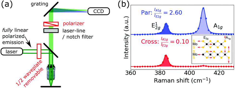 | ||
| Fig. 2 (a) The key components of a Raman setup with the additional elements needed to perform polarized measurements highlighted in red. The output of the laser is assumed to be linearly polarized e.g. achieved by a polarizer (not shown). (b) The polarized Raman response of a thick MoS2 flake obtained by exfoliation measured in the parallel polarization (upper spectrum) and the cross polarized (lower spectrum) configuration showing the dominant A1g and E12g peaks. Notice the non-zero A1g peak in the spectrum measured in the cross polarized configuration. This non-zero response is in a large part caused by the non-zero E field in the z direction due to the relatively high numerical aperture used in the experiments. The inset shows an Illustration of the A1g and E12g vibrational modes in a bilayer of MoS2. | ||
To complete the model, an accurate description of the electric fields is needed. In a typical far-field Raman setup a high numerical aperture (NA) microscope objective is used to efficiently probe the Raman response of solids. The electric fields in the focal plane of such a high NA objective are quite complex as shown by Turrell et al.44,45 For example, a significant electric field in the propagation direction of the light is present for high NA.44,45,57 The impact of this effect can be seen in Fig. 2 contributing significantly to the non-zero A1g response in the cross polarized configuration which increases with higher NA, an effect also observed for other materials.44 Hence, the direction and magnitude of the electric field in the spot have to be taken into account and cannot be assumed to be purely in-plane. The description of the electric fields introduced by Boivin and Wolf was used in this work together with the approach taken by Turrell et al. to describe the collection of the light and Gaussian intensity profile of the laser.44,45,57
The Raman response of nanocrystalline TMDs can now be calculated by summing up the individual responses of grains described by eqn (1) and the full equations can be written down. However, instead of summing over the individual grains, it is more convenient to integrate over all possible orientations and introduce an angular grain distribution “weighting” function W(θ,ψ,ϕ) which represents the fraction of the grains with a specific crystal orientation θ,ψ,ϕ. In most cases the in-plane orientation of the grains is randomly distributed – i.e. a texture similar to the fibre texture for thin-films34 – and the weighting function can be simplified to W(θ) with θ the angle between the z-direction and the c-axis of the grain; illustrated in Fig. 3 for several relevant distributions. The Raman response of a nanocrystalline material can now be written as an integral over the θ,ψ,ϕ angles sampling all possible grain orientations (weighted using the W(θ,ψ,ϕ) function) together with the aforementioned description of the electric fields which also consists of two sets of integrals. The intensity I of a Raman mode x due to tensor Rx of a nanocrystalline material with angular grain distribution W(θ,ψ,ϕ) probed in the back-scattering geometry is given by
 | (2) |
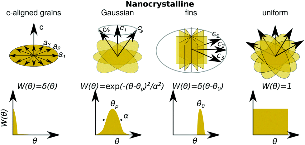 | ||
| Fig. 3 (top row) Illustration of the different textures and (bottom row) the associated angular distributions functions for different textures. From left to right, nanocrystalline material consisting of in-plane oriented grains, grains with a Gaussian distribution, out-of-plane oriented grains, and a uniform distribution are shown. Except for the angle θ, i.e. the angle between the c-axis and the z direction, all orientations are assumed to be equally likely. | ||
To ascertain the impact of the angular grain distribution on the Raman response, the MoS2 case is studied in more detail. The model is used to predict the Raman response of nanocrystalline MoS2 considering different angular grain distributions. The exact values of the elements of Rx tensors describing the A1g and E12g vibrations were determined from a reference measurement on a thick exfoliated MoS2 flake in the cross and the parallel polarized configuration. The two measured spectra yield 4 data points for 4 unknown tensor components, see also the ESI.†58 Once the tensor elements are known for both vibrations, the strength of the A1g and E12g modes for both polarization configurations can be calculated for different angular grain distributions. In practice, the ratio of the A1g and E12g contributions is a more robust metric and therefore a mapping of the A1g/E12g ratio onto the parameters of the distribution was calculated for: (i) the delta distribution, (ii) the uniform distribution, and (iii) the Gaussian distribution.
Fig. 4 shows the mapping of the A1g/E12g ratio calculated for MoS2 described by the Gaussian distribution for the parallel and cross polarized configuration, see the ESI† for NAs other than 0.75.58 The A1g/E12g ratio calculated for the delta distribution, also shown in Fig. 4, overlaps with the ratio described by the Gaussian angular distribution at α → 0, demonstrating the consistency of the model for the two different distributions. The non-polarized case is qualitatively similar to the parallel polarized configuration but it is not shown since the measured A1g/E12g ratio by a non-polarized setup depends on the Raman instrument. Turning our attention to the magnitude of the variation in the A1g/E12g ratio for the polarized configurations, it can be seen in Fig. 4 that this variation is quite significant. In most cases the effect of texture dominates over other effects such as defect density and strain.21,35,59 This observation underlines the importance of texture and, more specifically, the angular grain distribution in interpreting the Raman response of nanocrystalline TMDs.
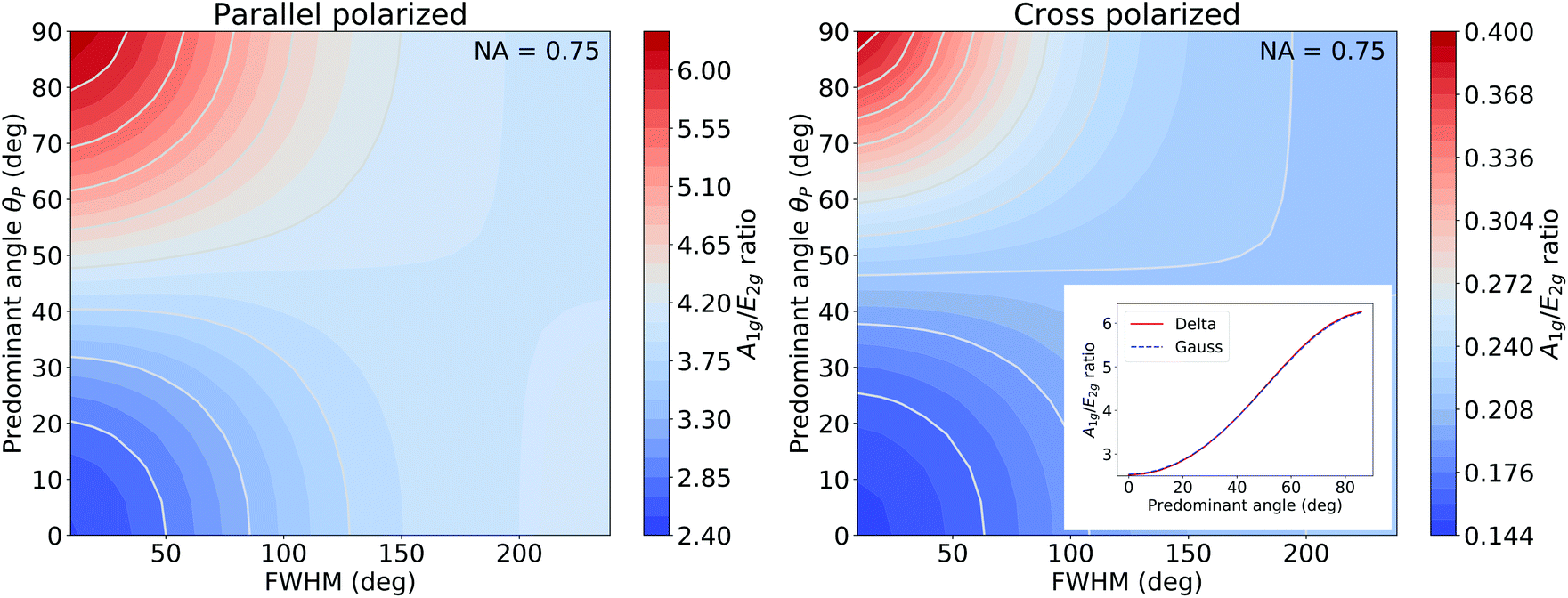 | ||
| Fig. 4 The A1g/E12g ratio of MoS2 as a function of the FWHM and predominant angle of the Gaussian grain distribution for (left) the parallel and (right) cross polarized Raman configuration in a backscattering geometry utilizing a 50× objective and a numerical aperture of 0.75. The insert shows the overlap for the delta distribution and the Gaussian distribution with a negligible FWHM of the A1g/E12g ratio as a function of the predominant angle. | ||
Fig. 4 can also be used to determine the angular grain distribution from two complementary polarized Raman measurements. Each measured A1g/E12g ratio describes a curve in the mapping in either the parallel or cross polarized configuration. The point where these two curves intersect represents the angular grain distribution of the sample. If the two lines do not intersect, the angular grain distribution cannot be described by a single Gaussian distribution. Furthermore, this also illustrates why it is in general not possible to uniquely determine the angular grain distribution from a single (unpolarized) Raman spectrum. A single measurement does not describe a point but a line in Fig. 4 and hence does not uniquely characterize the angular grain distribution. Furthermore, the A1g/E12g peak ratio measured by an unpolarized Raman measurements varies from setup to setup making interpretation difficult. See the ESI† for more details on: the impact of e.g. strain and grain size, the impact of the NA on the A1g/E12g peak ratio, and a discussion of unpolarized versus polarized peak-ratio measurements. To summarize, the modelling showed that the angular grain distribution has a significant impact on the A1g/E12g ratio which cannot be neglected and insight into the angular grain distribution can be gained by measuring at least two complementary polarized Raman spectra.
Most nanocrystalline samples will have an angular grain distribution that is more complex than a single Gaussian function. If the mismatch between the actual distribution and the Gaussian distribution is large, there will be no solution or in other words, the lines described by the measured A1g/E12g ratios for the parallel and cross polarized configuration do not intersect. Typically, thicker synthesized MoS2 films have predominantly in-plane oriented grains near the interface with the substrate, while the top layer is dominated by OoPO grains. Fig. 5 shows an X-TEM image of such a film, combined with an angular grain distribution determined by a 2D-Fourier transform analysis of this image. The quantitative interpretation of the angular grain distribution obtained in this fashion is not straight forward and will be discussed later but qualitatively it does show the complexity of the W(θ) function. To represent this richer texture, the Raman response can be described by a weighted sum of two contributions: a contribution representing the in-plane grains (θp = 0°) and a contribution for the OoPO grains (θp = 90°). This “two-layer” approach to model the angular grain distribution is used throughout this work to determine the OoPO material fraction from the Raman data and it is quite similar in concept to the texture coefficients used in the field of X-ray diffraction.34
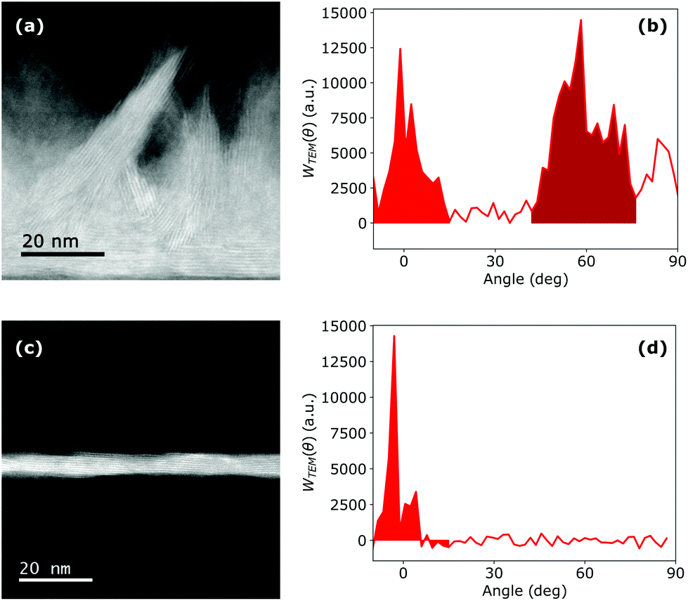 | ||
| Fig. 5 (a) Cross-section HAADF image of a MoS2 film grown with 200 cycles of PE-ALD clearly showing the in-plane oriented grains near the interface with the substrate and the further evolution of the texture to out-of-plane oriented grains near the surface. (b) Angular grain distribution associated with this specific TEM image with the contribution of the horizontal layers at angle 0° and the largest fin at 55°. Because of the limited field-of-view only a few out-of-plane grains are present in the image and, as a result, these large out-of-plane grains dominate the W(θ) function leading to relatively narrow peaks. (c) Cross-section HR-STEM image of a thermally sulphurized MoOx film showing predominantly horizontally oriented grains and (d) the associated angular grain distribution. | ||
Texture evolution during PE-ALD growth of MoS2 studied by polarized Raman spectroscopy
The evolution of the texture of PE-ALD grown MoS2 was studied as a function of thickness (i.e. the number of ALD cycles) using polarized Raman spectroscopy and selected samples were also measured with complementary techniques. This allows the validation of the texture obtained with polarized Raman spectroscopy and, at the same time, provides insight into the crystal growth. From our earlier work, it is already known that the texture of MoS2 grown by PE-ALD shows predominantly in-plane oriented grains for thin films and changes into a texture with OoPO grains on top when growing thick films.15 MoS2 films were synthesized on a Si(100)/450 nm SiO2 substrate by performing 15, 20, 50, 100, 200, and 500 cycles of the PE-ALD process at 450 °C as described by Sharma et al.15 This resulted in MoS2 films of 1.2, 1.6 nm, 4.0 nm, 8.0 nm, 16 nm and ∼40 nm thick, respectively.Fig. 6 shows the Raman spectra of four of these MoS2 films measured in both the parallel and cross polarized configuration. The same A1g and E12g peaks are present for both the exfoliated MoS2 (Fig. 2) and the synthesized material (Fig. 6), with the latter showing slightly larger peak broadening. Synthesized TMDs commonly show this larger peak broadening and a higher A1g-to-E12g separation (for the same thickness), most likely caused by effects such as finite grain size and peak shift due to strain averaged over many grains.60,61 To quantify the Raman spectra further, the A1g/E12g peak ratio was determined from the peak area by fitting both the A1g and the E12g peaks with two Voigt peaks each, as is commonly practice.20,35Table 1 lists the measured A1g/E12g peak ratio obtained using this procedure. For the PE-ALD MoS2 films, a decrease in the A1g/E12g ratio was observed for both polarization modes with increasing film thickness up to 100 cycles. Above 100 cycles, the A1g/E12g ratio increases again for both polarization configurations. The A1g/E12g ratio found for the 500 cycles sample in the cross polarized configuration shows a large jump which is most likely caused by both the increasing OoPO fraction and an increase in scattering causing depolarization. Based upon the trend in the A1g/E12g ratio, we can qualitatively conclude that the texture of the ALD grown films starts out (to a degree) OoPO and becomes more akin to that of the exfoliated material up to 100 cycles, then the texture starts to become more OoPO oriented again. To quantify the trend in the Raman spectra, the measured A1g/E12g ratios were fitted to the 2-layer model. In this fit, the adjustable parameters of the 2-layer model were determined by minimizing the sum of the square of the difference between the measured and modelled A1g/E12g ratios. The fraction of out-of-plane to in-plane oriented grains found with this procedure is listed in Table 1 and shows a decreasing from 0.68 for the thinnest film up to 0.45 for the 100 cycles sample. Thicker films again show an increase in OoPO fraction up to 0.55 for the film grown by 200 cycles.
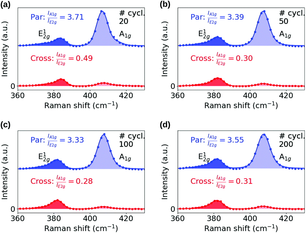 | ||
| Fig. 6 The polarized Raman response of MoS2 films grown by (a) 20, (b) 50, (c) 100, (d) 200 cycles of PE-ALD. For each sample, the response in both the parallel (upper spectrum) and the cross (lower spectrum) polarized configuration in shown. The A1g/E12g peak ratios calculated from the fit (solid line) to the data (markers) are also shown for both polarization configurations. | ||
| Sample description | Thickness | Ratio A1g/E12g | OoPO quantification | ||||
|---|---|---|---|---|---|---|---|
| Parallel | Cross | Raman | X-TEM | XRD Tf100 | 2D GIXD | ||
| Exfoliated | ≫1 ml | 2.60 ± 0.05 | 0.10 ± 0.02 | 0% | — | — | — |
| Sulphurized MoOx | 8.0 ± 0.5 nm | 2.99 | 0.19 | <5% | 0% ± 10% | — | — |
| PE-ALD 450 °C | 500c | 3.89* | 1.82* | — | — | 0.43 | 68 ± 10% |
| 200c | 3.55 | 0.31 | 55% | 75% | 0.24 | 47% | |
| 100c | 3.33 | 0.28 | 45% | — | — | — | |
| 50c | 3.39 | 0.30 | 49% | — | — | — | |
| 20c | 3.71 | 0.49 | 68% | — | — | — | |
| 15c | 4.84 | 0.70** | — | — | — | — | |
| PE-ALD & H2S Annealed | 20c | 2.77 | 0.10 | <5% | — | — | — |
| 50c | 2.47 | 0.09 | <5% | — | — | — | |
The Raman approach was validated by contrasting the OoPO fraction determined from the Raman spectra to the texture measured by complementary diagnostics on selected samples. The cross-section TEM (X-TEM) measurement performed on a thick (200 cycles) PE-ALD grown MoS2 film, see Fig. 5, showed a significant amount of OoPO grains on top of the in-plane oriented grains; qualitatively in-line with the OoPO fraction determined using Raman spectroscopy. To quantify the TEM results, a Fourier analysis was performed on the image determining the angular grain distribution shown in Fig. 5(b), for more details see S5 of the ESI.† The interpretation of the OoPO fraction obtained by this approach and how it compares to the TEM study is nuanced: for example, small grains (e.g. <2 nm) are under sampled in TEM because of limited contrast but will contribute significantly to the OoPO fraction measured by Raman. As such, an absolute interpretation of the OoPO fraction as a volume fraction of grains for either TEM or Raman spectroscopy is not straightforward. Nevertheless, an out-of-plane fraction of 0.55 for the 200 cycles PE-ALD sample is comparable to the estimated OoPO fraction of 0.75 from the TEM analysis especially considering the bias to visually appealing images. Similarly, the MoS2 film obtained by sulfurization of MoOx, discussed in more detail later, showed virtually no OoPO material in both the X-TEM and Raman measurements. Electron backscatter diffraction (EBSD) was not feasible due to the small grain size (∼10 nm) and electron diffraction by TEM was found to be relatively insensitive to the OoPO material. XRD measurements in the Bragg Brentano configuration only showed the 002 reflection for thin (from monolayer up to 10 nm), if any, despite both crystalline in-plane and OoPO material being present.15 For thicker films grown by 200 and 400 cycles PE-ALD, the XRD patterns did shown the 002 reflection (associated with in-plane material), the 100 reflections and to a lesser extent the 101 reflection (both associated with OoPO material) allowing texture factors to be determined. The texture factor for the 100 peak is listed in Table 1 and it is a measure for the fraction of the 100 texture. A higher texture factor indicates a stronger texture of that specific orientation, but it cannot directly be associated with a volume fraction of OoPO material. That said, the increase in the degree of 100 texture with increasing thickness measured by XRD is in-line with the increase in the fraction of OoPO material observed from the Raman analysis. 2D grazing-incidence X-ray diffraction (2D GIXD) measurements using synchrotron radiation (1.4 Å) at incidence angles of 0.2° and 1° were also performed on MoS2 films grown by 200 and 500 cycles of PE-ALD at 450 °C. Fig. 7 shows a typical 2D GIXD pattern recorded at the 1.0° incidence angle, probing the full depth of the film, showing diffraction peaks associated with the 2H-MoS2 crystal structure. The most prominent peaks for texture determination can be found at |q| = 1 Å−1, with the in-plane oriented material ((100) plane parallel to the substrate surface) contributing to the signal at qxy = 0 and the OoPO material ((100) plane perpendicular to the substrate surface) contributing to the signal at qz ∼ 0. On the other hand, the 0.2° measurement only probes the top section of the MoS2 film and showed predominantly OoPO material, see also S6 of the ESI.†58 This indicates that the OoPO material is predominantly located at the surface, in-line with the X-TEM images. The OoPO fraction can be determined from the GIXD measurement at 1° from a further analysis of the GIXD data. Fig. 7(b) shows the angular grain distribution of the two samples determined from a pole-figure analysis of the GIXD data recorded at 1.0°. From this angular grain distribution, an OoPO fraction of 0.47 and 0.68 was found for the 200 and 500 cycles sample, respectively. The good agreement between the Raman and GIXD results should be seen in the context of the significant uncertainty in the absolute value of the OoPO fraction present in either approach and should therefore not be over interpreted Moreover, each of these diagnostics probes an overlapping but slightly different subset of the material due to its own “selection” rules. The trend in the data, on the other hand, is expected to be accurate and all approaches do indeed show the same trend in the OoPO fraction with thickness. This data set showed that polarized Raman spectroscopy is capable of rapidly (<30 s) characterizing the texture of the MoS2 films across a wide thickness range of 2 up to 20 nm. As such, polarized Raman spectroscopy can be used to differentiate between films with and without OoPO material even for few-layer MoS2 films, i.e. the fast screening of synthesized material.
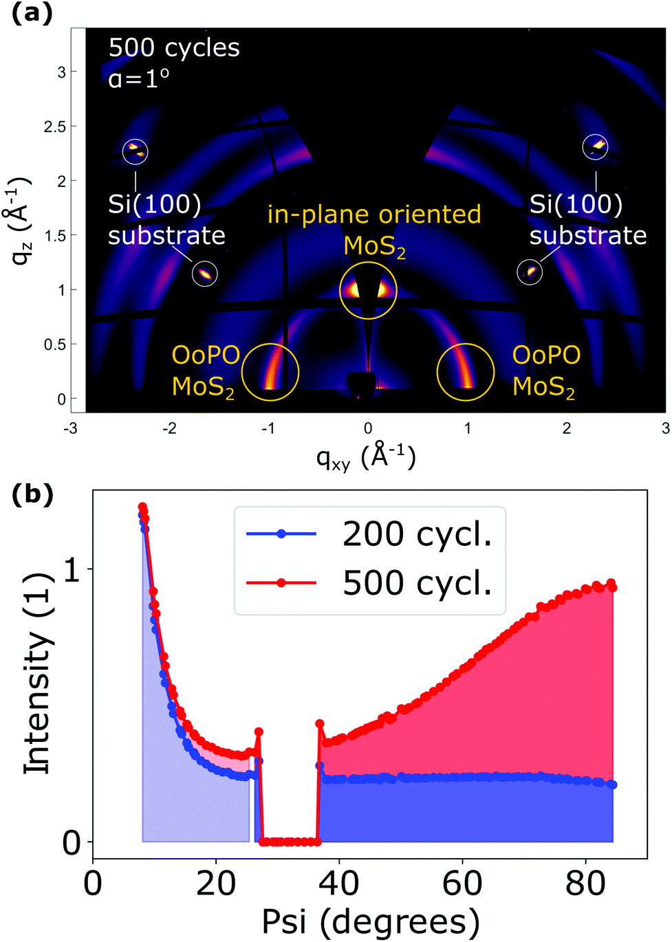 | ||
| Fig. 7 (a) 2D GIXD diffraction pattern of a MoS2 film grown by 500 cycles of PE-ALD at 450 °C using an incident angle α of 1.0°. The radial profile of e.g. the 002 reflection at |q| = ∼1 Å−1 reveals the texture of the MoS2 films. The diffraction pattern shown here is the sum of 180 individual GIXD diffraction patterns measured at different azimuths phi (rotation around the surface normal). For both samples, no significant variation was observed as a function of phi and the pole figures calculated from the individual patterns further confirmed the fibre texture of the samples. (b) Angular grain distribution for the MoS2 films grown by 200 and 500 cycles of ALD deduced from the pole diagrams. | ||
The OoPO fraction reported in Table 1 for the ALD thickness series also provides evidence for the growth mechanism put forward by us and others during ALD, highlighting the value of texture data. In our previous work we presented a model predominantly based upon TEM studies in which we proposed that the formation of horizontal grains occurs first followed by the development of OoPO material most likely at the point where the horizontal grains meet (after about 10 cycles).15 For the initial stages of growth of the related ALD process of WS2, Groven et al. proposed that these horizontal grains most likely form due to coalescence of small highly mobile clusters on the surface during the first few cycles.62 The growth proceeds predominantly on the edges of the large grains once these are established. The insights into the angular grain distribution obtained in this work confirm and complement these models: the polarized Raman data suggests that the small clusters that precede the grain formation have a fairly random orientation. With the formation of larger horizontal grains the texture of the material becomes more akin to that of exfoliated material, evidenced by the decrease in the OoPO fraction with thickness up to 100 cycles. For films grown by more than 100 cycles an increase in the OoPO fraction was found from the polarized Raman data, in line with the formation of fins as seen in Fig. 5.
Texture of sulphurized MoOx and H2S annealed MoS2
Fig. 8(a) shows the Raman spectra of a MoOx film sulphurized an H2S environment at 900 °C. The Raman response of the MoOx based film showed A1g/E12g ratios quite close to that of the exfoliated MoS2. This implies that the material consists predominantly of in-plane oriented grains and the analysis of the Raman spectra revealed an OoPO fraction <5% in both cases. This is in line with the in-plane oriented grains of MoS2 observed by X-TEM shown in Fig. 5(c) of a similar sample. In a separate experiment, the change in texture in two PE-ALD MoS2 films caused by annealing in the same H2S environment was investigated by Raman. Comparing the Raman spectra of the MoS2 film grown by PE-ALD before (Fig. 6(a and b)) and after the H2S anneal (Fig. 8(b and c)) revealed a significant change in the A1g/E12g ratio, indicating a conversion of OoPO grains into in-plane oriented grains. The 2-layer model was applied to these two cases and the results are listed in Table 1. For the PE-ALD MoS2 films, a decrease in the out-of-plane fraction from 49% and 68% down to <5% was observed. The change in texture due to the H2S anneal is also reflected in the photoluminescence (PL) response. For the 20 cycles MoS2 films a significant improvement was observed in the PL response which improved by a factor of 6.5 upon annealing, see Fig. 8(d).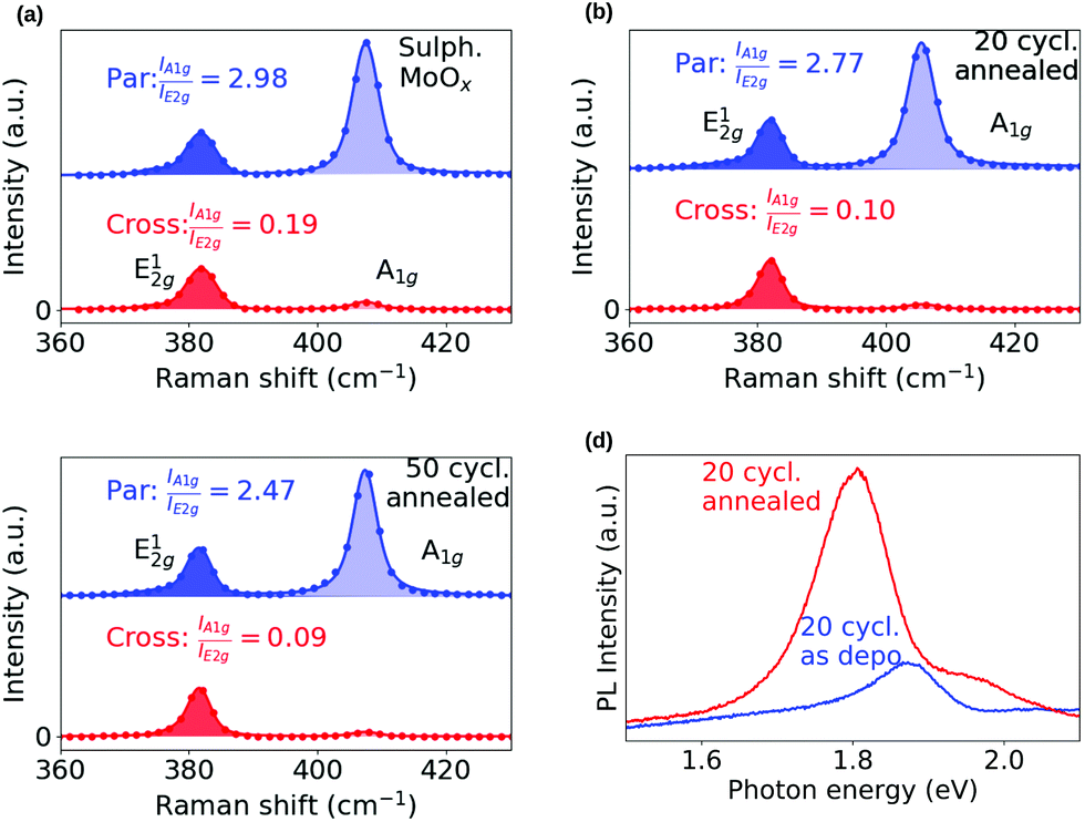 | ||
| Fig. 8 The polarized Raman response of MoS2 synthesized by: (a) sulphurization of ALD MoOx, (b) annealing of the MoS2 grown by 20 cycles (as deposited shown in Fig. 6(a)) and (c) 50 cycles PE-ALD (as deposited shown in Fig. 6(b)) after an anneal in H2S. For each sample, the response in both the parallel (upper spectrum) and the cross (lower spectrum) polarized configuration in shown. The A1g/E12g peak ratio calculated from the fit (solid line) to the data (markers) is also included. (d) The PL response of the same 20 cycles PE-ALD MoS2 film deposited by PE-ALD as-deposited and after the anneal step. | ||
Conclusion
We have gained fundamental insight into the influence of texture on the Raman response of nanocrystalline TMDs. An accurate description of the impact of the angular grain distribution of nanocrystalline TMDs on the (polarized) Raman response was derived. A variation of approximately a factor 3 in the A1g/E12g ratio in the Raman response was predicted for the particular case of MoS2 when going from a predominantly in-plane texture to out-of-plane oriented material. This model can also be used to predict the impact of texture on other TMDs with the D3h/D6h symmetry and for other classes of material without any modifications. Furthermore, we have shown that our model can be used to determine the angular grain distribution from the measured polarized Raman response which was validated on several MoS2 films with textures ranging from in-plane to out-of-plane material. Good agreement was found between the angular grain distribution determined from the Raman spectra and the texture determined from cross-sectional TEM, XRD, and 2D GIXD. The main benefit of probing texture with Raman spectroscopy over established techniques, such as XRD and TEM, is that this approach is non-destructive, it requires (virtually) no sample preparation, and its short measurement time. Moreover, the typical ease-of-use of Raman spectroscopy and the capability to obtain spatial mappings are undiminished and also apply to the texture determination presented here. For material growth studies, polarized Raman spectroscopy will allow the monitoring of the crystallization and texture during film growth (i.e. kinetics). In future work, we will generalize our model to also describe the nonlinear optical response of nanocrystalline materials such as second-harmonic generation (SHG).Methods
Polarized Raman setup
The Raman spectra in this work were collected using a Renishaw inVia confocal Raman microscope. All measurements were performed with a 415 nm laser using a Leica N Plan EPI 50× objective with a NA of 0.75 in conjunction with an 1800 lines per mm grating. For each measurement, ten spectra were acquired with an integration time of 10 seconds each and a laser power of ∼0.2 mW focused on a ∼1 μm diameter spot. For the polarized measurements the input polarization was varied whereas the detected polarization was kept constant. This is important since the efficiency of the grating and the sensitivity of CCD camera can vary an order of magnitude for p and s polarization depending on the specific setup. The variation in input power due to the switching of the input polarization state was found to be minimal (<1% judging from the E12g intensity). Moreover, variation in input power below the aforementioned laser power did not affect the A1g/E12g ratio.Synthesis and H2S treatment of MoS2 films & characterization
The PE-ALD films were grown at 450 °C using the procedure detailed in the work on Sharma et al. on Si(100) wafers with a 450 nm thermal SiO2 film on top obtained from SIEGERT WAFER GmbH.15 The subsequent anneal of the MoS2 films in the H2S atmosphere was performed at 900 °C for 45 minutes in a Ar + 10% H2S flow using a ramp rate of 10 °C min−1 dwelling the sample at 150 °C for 15 minutes. MoOx films were grown with the PE-ALD process as described by Vos et al. after which the films were sulphurized using the same procedure.63 The thickness of the MoS2 films was determined using a Woollam M2000D spectroscopic ellipsometer employing a B-spline model for the optical properties of the MoS2 film. The TEM images were obtained using a probe corrected JEOL ARM 200F operated at 80 kV. Cross-sectional preparation of the TEM samples was performed using a standard lift-out Focused Ion Beam (FIB) procedure. The GIXD measurements were conducted at the Elettra XRD1-beamline in Trieste, Italy. The experiments were performed with X-rays with a wavelength of 1.4 Å while the incident angle α was set to either 0.2 or 1.0 degrees to vary the penetration depth into the sample. The intensity of the scattered X-rays was measured using a Pilatus 2M detector situated approximately 150 mm after the sample. To obtain information about the crystallites’ in-plane orientation, the sample was rotated around its surface normal during exposure and 180 separate images were recorded, each integrating two degrees of the sample rotation. The software package GIDVis was used for data conversion to reciprocal space, general data analysis and to extract the pole diagrams figures from the 2D GIXD data.64Conflicts of interest
There are no conflicts to declare.Acknowledgements
This work has been partially funded by the Electronic Component Systems for European Leadership Joint Undertaking under grant agreement No. 692527. This Joint Undertaking receives support from the European Union's Horizon 2020 research and innovation programme and the Netherlands, Belgium, France, Hungary, Ireland, Denmark, Israel. This work has also been supported by the European Research Council (Grant Agreement No. 648787-ALD of 2DTMDs). Solliance and the Dutch province of Noord-Brabant are acknowledged for funding the TEM facility. Mrs Barcones is acknowledged for FIB preparation of the TEM sample. We acknowledge the Elettra Synchrotron Trieste for beamtime allocation and thank Luisa Barba for assistance in using beamline XRD1. The authors are grateful for assistance performed by Dr Hofmann, Dr Wu, and Y. Zhang performing the high temperature H2S treatment of the samples.References
- R. Kappera, D. Voiry, S. E. Yalcin, B. Branch, G. Gupta and A. D. Mohite, et al., Phase-engineered low-resistance contacts for ultrathin MoS2 transistors, Nat. Mater., 2014, 13, 1–15, DOI:10.1038/nmat4080.
- Y. R. An, X. L. Fan, Z. F. Luo and W. M. Lau, Nanopolygons of monolayer MoS2: Best morphology and size for HER catalysis, Nano Lett., 2017, 17, 368–376, DOI:10.1021/acs.nanolett.6b04324.
- D. Merki and X. Hu, Recent developments of molybdenum and tungsten sulfides as hydrogen evolution catalysts, Energy Environ. Sci., 2011, 4, 3878–3888, 10.1039/C1EE01970H.
- A. Y. S. Eng, A. Ambrosi, Z. Sofer, P. Šimek and M. Pumera, Electrochemistry of transition metal dichalcogenides: strong dependence on the metal-to-chalcogen composition and exfoliation method, ACS Nano, 2014, 8, 12185–12198, DOI:10.1021/nn503832j.
- K. Kang, S. Xie, L. Huang, Y. Han, P. Y. Huang and K. F. Mak, et al., High-mobility three-atom-thick semiconducting films with wafer-scale homogeneity, Nature, 2015, 520, 656–660, DOI:10.1038/nature14417.
- B. Radisavljevic, A. Radenovic, J. Brivio, V. Giacometti and A. Kis, Single-layer MoS2 transistors, Nat. Nanotechnol., 2011, 6, 147–150, DOI:10.1038/nnano.2010.279.
- N. Huo, J. Kang, Z. Wei, S.-S. Li, J. Li and S.-H. Wei, Novel and Enhanced Optoelectronic Performances of Multilayer MoS2 -WS2 Heterostructure Transistors, Adv. Funct. Mater., 2014, 24, 7025–7031, DOI:10.1002/adfm.201401504.
- K. F. Mak and J. Shan, Photonics and optoelectronics of 2D semiconductor transition metal dichalcogenides, Nat. Photonics, 2016, 10, 216, DOI:10.1038/nphoton.2015.282.
- S. Das, H.-Y. Chen, A. V. Penumatcha and J. Appenzeller, High performance multilayer MoS2 transistors with scandium contacts, Nano Lett., 2013, 13, 100–105, DOI:10.1021/nl303583v.
- H. Wang, L. Yu, Y.-H. Lee, Y. Shi, A. Hsu and M. L. Chin, et al., Integrated circuits based on bilayer MoS2 transistors, Nano Lett., 2012, 12, 4674–4680, DOI:10.1021/nl302015v.
- W. Bao, X. Cai, D. Kim, K. Sridhara and M. S. Fuhrer, High mobility ambipolar MoS2 field-effect transistors: Substrate and dielectric effects, Appl. Phys. Lett., 2013, 102, 042104, DOI:10.1063/1.4789365.
- D. Kong, H. Wang, J. J. Cha, M. Pasta, K. J. Koski and J. Yao, et al., Synthesis of MoS2 and MoSe 2 Films with Vertically Aligned Layers, Nano Lett., 2013, 13, 1341–1347, DOI:10.1021/nl400258t.
- D. Merki, S. Fierro, H. Vrubel and X. Hu, Amorphous molybdenum sulfide films as catalysts for electrochemical hydrogen production in water, Chem. Sci., 2011, 2, 1262–1267, 10.1039/C1SC00117E.
- W. Jeon, Y. Cho, S. Jo, J.-H. Ahn and S.-J. Jeong, Wafer-Scale Synthesis of Reliable High-Mobility Molybdenum Disulfide Thin Films via Inhibitor-Utilizing Atomic Layer Deposition, Adv. Mater., 2017, 29, 1703031, DOI:10.1002/adma.201703031.
- A. Sharma, M. A. Verheijen, L. Wu, S. Karwal, V. Vandalon and H. C. M. Knoops, et al., Low-temperature plasma-enhanced atomic layer deposition of 2-D MoS2: large area, thickness control and tuneable morphology, Nanoscale, 2018, 10, 8615–8627, 10.1039/c8nr02339e.
- G. Deokar, D. Vignaud, R. Arenal, P. Louette and J. F. Colomer, Synthesis and characterization of MoS2 nanosheets, Nanotechnology, 2016, 27, 10, DOI:10.1088/0957-4484/27/7/075604.
- M. Mattinen, T. Hatanpää, T. Sarnet, K. Mizohata, K. Meinander and P. J. King, et al., Atomic Layer Deposition of Crystalline MoS2 Thin Films: New Molybdenum Precursor for Low-Temperature Film Growth, Adv. Mater. Interfaces, 2017, 4, 1700123, DOI:10.1002/admi.201700123.
- M. Rahaman, R. D. Rodriguez, G. Plechinger, S. Moras, C. Schüller and T. Korn, et al., Highly Localized Strain in a MoS2/Au Heterostructure Revealed by Tip-Enhanced Raman Spectroscopy, Nano Lett., 2017, 17, 6027–6033, DOI:10.1021/acs.nanolett.7b02322.
- W. M. Parkin, A. Balan, L. Liang, P. M. Das, M. Lamparski and C. H. Naylor, et al., Raman Shifts in Electron-Irradiated Monolayer MoS2, ACS Nano, 2016, 10, 4134–4142, DOI:10.1021/acsnano.5b07388.
- C. Lee, H. Yan, L. E. Brus, T. F. Heinz, J. Hone and S. Ryu, Anomalous lattice vibrations of single- and few-layer MoS2, ACS Nano, 2010, 4, 2695–2700, DOI:10.1021/nn1003937.
- Y. Wang, C. Cong, C. Qiu and T. Yu, Raman spectroscopy study of lattice vibration and crystallographic orientation of monolayer mos2 under uniaxial strain, Small, 2013, 9, 2857–2861, DOI:10.1002/smll.201202876.
- M. H. Heyne, J.-F. de Marneffe, I. Radu, E. C. Neyts and S. De Gendt, Thermal recrystallization of short-range ordered WS2 films, J. Vac. Sci. Technol., A, 2018, 36, 05G501, DOI:10.1116/1.5036654.
- B. Groven, M. Heyne, A. Nalin Mehta, H. Bender, T. Nuytten and J. Meersschaut, et al., Plasma-Enhanced Atomic Layer Deposition of Two-Dimensional WS2 from WF6, H2 Plasma, and H2S, Chem. Mater., 2017, 29(7), 2927–2938, DOI:10.1021/acs.chemmater.6b05214.
- J. Zhang, H. Yu, W. Chen, X. Tian, D. Liu and M. Cheng, et al., Scalable growth of high-quality polycrystalline MoS(2) monolayers on SiO(2) with tunable grain sizes, ACS Nano, 2014, 8, 6024–6030, DOI:10.1021/nn5020819.
- R. Ionescu, W. Wang, Y. Chai, Z. Mutlu, I. Ruiz and Z. Favors, et al., Synthesis of Atomically Thin MoS2 Triangles and Hexagrams and Their Electrical Transport Properties, IEEE Trans. Nanotechnol., 2014, 13, 749–754, DOI:10.1109/TNANO.2014.2319081.
- S. Wang, Y. Rong, Y. Fan, M. Pacios, H. Bhaskaran and K. He, et al., Shape Evolution of Monolayer MoS2 Crystals Grown by Chemical Vapor Deposition, Chem. Mater., 2014, 26, 6371–6379, DOI:10.1021/cm5025662.
- T. A. Ho, C. Bae, S. Lee, M. Kim, J. M. Montero-Moreno and J. H. Park, et al., Edge-On MoS2 Thin Films by Atomic Layer Deposition for Understanding the Interplay between the Active Area and Hydrogen Evolution Reaction, Chem. Mater., 2017, 29(17), 7604–7614, DOI:10.1021/acs.chemmater.7b03212.
- N. Choudhary, J. Park, J. Y. Hwang and W. Choi, Growth of Large-Scale and Thickness-Modulated MoS2 Nanosheets, ACS Appl. Mater. Interfaces, 2014, 6, 21215–21222, DOI:10.1021/am506198b.
- H. Li, H. Wu, S. Yuan and H. Qian, Synthesis and characterization of vertically standing MoS2 nanosheets, Sci. Rep., 2016, 6, 21171, DOI:10.1038/srep21171.
- F. Lan, Z. Lai, Y. Xu, H. Cheng, Z. Wang and C. Qi, et al., Synthesis of Vertically Standing MoS2 Triangles on SiC, Sci. Rep., 2016, 6, 31980, DOI:10.1038/srep31980.
- F. Zhang, K. Momeni, M. A. AlSaud, A. Azizi, M. F. HaineyJr and J. M. Redwing, et al., Controlled synthesis of 2D transition metal dichalcogenides: from vertical to planar MoS2, 2D Mater., 2017, 4, 025029, DOI:10.1088/2053-1583/aa5b01.
- T. J. Wieting and M. Schlüter, Electrons and Phonons in Layered Crystal Structures, Springer Science & Business Media, 2012. Available: https://market.android.com/details?id=book-FpzqCAAAQBAJ Search PubMed.
- H. Wang, Z. Lu, S. Xu, D. Kong, J. J. Cha and G. Zheng, et al., Electrochemical tuning of vertically aligned MoS2 nanofilms and its application in improving hydrogen evolution reaction, Proc. Natl. Acad. Sci. U. S. A., 2013, 110, 19701–19706, DOI:10.1073/pnas.1316792110.
- M. Birkholz, Thin Film Analysis by X-Ray Scattering, John Wiley & Sons, 2006. Available: https://market.android.com/details?id=book-qZ5CSSV1rNAC Search PubMed.
- S. Mignuzzi, A. J. Pollard, N. Bonini, B. Brennan, I. S. Gilmore and M. A. Pimenta, et al., Effect of disorder on Raman scattering of single-layer MoS2, Phys. Rev. B: Condens. Matter Mater. Phys., 2015, 91, 1–7, DOI:10.1103/PhysRevB.91.195411.
- Y. Zhao, X. Luo, H. Li, J. Zhang, P. T. Araujo and C. K. Gan, et al., Interlayer breathing and shear modes in few-trilayer MoS2 and WSe2, Nano Lett., 2013, 13, 1007–1015, DOI:10.1021/nl304169w.
- X. Zhang, Q.-H. Tan, J.-B. Wu, W. Shi and P.-H. Tan, Review on the Raman spectroscopy of different types of layered materials, Nanoscale, 2016, 8, 6435–6450, 10.1039/C5NR07205K.
- H. Li, Q. Zhang, C. C. R. Yap, B. K. Tay, T. H. T. Edwin and A. Olivier, et al., From bulk to monolayer MoS2: Evolution of Raman scattering, Adv. Funct. Mater., 2012, 22, 1385–1390, DOI:10.1002/adfm.201102111.
- E. Mercado, A. Goodyear, J. Moffat, M. Cooke and R. S. Sundaram, A Raman metrology approach to quality control of 2D MoS2 film fabrication, J. Phys. D: Appl. Phys., 2017, 50, 184005, DOI:10.1088/1361-6463/aa6786.
- F. Zahid, L. Liu, Y. Zhu, J. Wang and H. Guo, A generic tight-binding model for monolayer, bilayer and bulk MoS2, AIP Adv., 2013, 3, 052111, DOI:10.1063/1.4804936.
- L. Liang and V. Meunier, First-principles Raman spectra of MoS2, WS2 and their heterostructures, Nanoscale, 2014, 6, 5394, 10.1039/c3nr06906k.
- Y. Jung, J. Shen, Y. Liu, J. M. Woods, Y. Sun and J. J. Cha, Metal seed layer thickness-induced transition from vertical to horizontal growth of MoS2 and WS2, Nano Lett., 2014, 14, 6842–6849, DOI:10.1021/nl502570f.
- C. Thomsen, R. Wegerer, H.-U. Habermeier and M. Cardona, Determination of the degree of epitaxy in high-Tc thin films by raman spectroscopy, Solid State Commun., 1992, 83, 199–203, DOI:10.1016/0038-1098(92)90837-Y.
- C. Bremard, P. Dhamelincourt, J. Laureyns and G. Turrell, Effect of High-Numerical-Aperture Objectives on Polarization Measurements in Micro-Raman Spectrometry, Appl. Spectrosc., 1985, 39, 1036–1039, DOI:10.1366/0003702854249754.
- G. Turrell, Analysis of polarization measurements in Raman microspectroscopy, J. Raman Spectrosc., 1984, 15, 103–108, DOI:10.1002/jrs.1250150207.
- G. Pezzotti and W. Zhu, Resolving stress tensor components in space from polarized Raman spectra: polycrystalline alumina, Phys. Chem. Chem. Phys., 2015, 17, 2608–2627, 10.1039/c4cp04244a.
- J. L. Verble and T. J. Wieting, Lattice Mode Degeneracy in MoS2 and Other Layer Compounds, Phys. Rev. Lett., 1970, 25, 362–365, DOI:10.1103/PhysRevLett.25.362.
- A. Molina-Sánchez and L. Wirtz, Phonons in single-layer and few-layer MoS2 and WS2, Phys. Rev. B: Condens. Matter Mater. Phys., 2011, 84, 155413, DOI:10.1103/PhysRevB.84.155413.
- X. Zhang, W. P. Han, J. B. Wu, S. Milana, Y. Lu and Q. Q. Li, et al., Raman spectroscopy of shear and layer breathing modes in multilayer MoS2, Phys. Rev. B: Condens. Matter Mater. Phys., 2013, 87, 115413, DOI:10.1103/PhysRevB.87.115413.
- J. Ribeiro-Soares, R. M. Almeida, E. B. Barros, P. T. Araujo, M. S. Dresselhaus and L. G. Cançado, et al., Group theory analysis of phonons in two-dimensional transition metal dichalcogenides, Phys. Rev. B: Condens. Matter Mater. Phys., 2014, 90, 115438, DOI:10.1103/PhysRevB.90.115438.
- M. Weber, in Raman Scattering in Materials Science, ed. W.H. Weber and R. Merlin, Springer-verlag, Berlin Heidelberg, 2000. DOI:10.1007/978-3-662-04221-2_3.
- M. Cardona, Resonance phenomena, in Light Scattering in Solids II: Basic Concepts and Instrumentation, ed. M. Cardona and G. Güntherodt, Springer, Berlin, Heidelberg, 1982, pp. 19–178. DOI:10.1007/3-540-11380-0_14.
- E. B. Wilson, J. C. Decius and P. C. Cross, Molecular Vibrations, Dover Publications Inc., 1980 Search PubMed.
- R. Loudon, The Raman effect in crystals, Adv. Phys., 1964, 13, 423–482, DOI:10.1080/00018736400101051.
- D. C. Harris and M. D. Bertolucci, Symmetry and Spectroscopy: An Introduction to Vibrational and Electronic Spectroscopy, Courier Corporation, 1978. Available: https://books.google.com/books/about/Symmetry_and_Spectroscopy.html?hl=&id=I3W6oSaRlMsC Search PubMed.
- X.-L. Liu, X. Zhang, M.-L. Lin and P.-H. Tan, Different angle-resolved polarization configurations of Raman spectroscopy: A case on the basal and edge plane of two-dimensional materials, Chin. Phys. B, 2017, 26, 067802, DOI:10.1088/1674-1056/26/6/067802.
- A. Boivin and E. Wolf, Electromagnetic Field in the Neighborhood of the Focus of a Coherent Beam, Phys. Rev., 1965, 138, B1561–B1565, DOI:10.1103/PhysRev.138.B1561.
- ESI.†.
- L. Yang, X. Cui, J. Zhang, K. Wang, M. Shen and S. Zeng, et al., Lattice strain effects on the optical properties of MoS2 nanosheets, Sci. Rep., 2015, 4, 5649, DOI:10.1038/srep05649.
- G. L. Frey, R. Tenne, M. J. Matthews, M. S. Dresselhaus and G. Dresselhaus, Raman and resonance Raman investigation of MoS2 nanoparticles, Phys. Rev. B: Condens. Matter Mater. Phys., 1999, 60, 2883–2892, DOI:10.1103/PhysRevB.60.2883.
- J. J. Pyeon, S. H. Kim, D. S. Jeong, S.-H. Baek, C.-Y. Kang and J.-S. Kim, et al., Wafer-scale growth of MoS2 thin films by atomic layer deposition, Nanoscale, 2016, 8, 10792–10798, 10.1039/c6nr01346e.
- B. Groven, A. Nalin Mehta, H. Bender, J. Meersschaut, T. Nuytten and P. Verdonck, et al., Two-Dimensional Crystal Grain Size Tuning in WS2 Atomic Layer Deposition: an Insight in the Nucleation Mechanism, Chem. Mater., 2018, 30(21), 7648–7663, DOI:10.1021/acs.chemmater.8b02924.
- M. F. J. Vos, B. Macco, N. F. W. Thissen, A. A. Bol and W. M. M. Kessels, Atomic layer deposition of molybdenum oxide from (NtBu)2(NMe2)2Mo and O2 plasma, J. Vac. Sci. Technol., A, 2016, 34, 01A103, DOI:10.1116/1.4930161.
- B. Schrode, S. Pachmajer, M. Dohr, C. Röthel, J. Domke, T. Fritz, R. Resel and O. Werzer, GIDVis – a Comprehensive Software Tool for Geometry-Independent Grazing-Incidence X-Ray Diffraction Data Analysis and Pole-Figure Calculations, J. Appl. Crystallogr., 2019, 52, 683–689, DOI:10.1107/S1600576719004485.
Footnote |
| † Electronic supplementary information (ESI) available: Impact of the Raman instrument and film imperfections on the A1g/E12g ratio, the full derivation of eqn (2) and a discussion about the determination of the Raman tensor elements, the TEM analysis, and more details about the GIXD measurements. See DOI: 10.1039/c9nr08750h |
| This journal is © The Royal Society of Chemistry 2019 |