
 Open Access Article
 This Open Access Article is licensed under a Creative Commons Attribution-Non Commercial 3.0 Unported Licence
Resolving single Cu nanoparticle oxidation and Kirkendall void formation with in situ plasmonic nanospectroscopy and electrodynamic simulations†
Sara
Nilsson
 a,
David
Albinsson
a,
Tomasz J.
Antosiewicz
b,
Joachim
Fritzsche
a and
Christoph
Langhammer
*a
a,
David
Albinsson
a,
Tomasz J.
Antosiewicz
b,
Joachim
Fritzsche
a and
Christoph
Langhammer
*a
aDepartment of Physics, Chalmers University of Technology, 412 96 Göteborg, Sweden. E-mail: clangham@chalmers.se
bFaculty of Physics, University of Warsaw, Pasteura 5, 02-093, Warsaw, Poland
First published on 16th October 2019
Abstract
Copper nanostructures are ubiquitous in microelectronics and heterogeneous catalysis and their oxidation is a topic of high current interest and broad relevance. It relates to important questions, such as catalyst active phase, activity and selectivity, as well as fatal failure of microelectronic devices. Despite the obvious importance of understanding the mechanism of Cu nanostructure oxidation, numerous open questions remain, including under what conditions homogeneous oxide layer growth occurs and when the nanoscale Kirkendall void forms. Experimentally, this is not trivial to investigate because when a large number of nanoparticles are simultaneously probed, ensemble averaging makes rigorous conclusions difficult. On the other hand, when (in situ) electron-microscopy approaches with single nanoparticle resolution are applied, concerns about beam effects that may both reduce the oxide or prevent oxidation via the deposition and cross-linking of carbonaceous species cannot be neglected. In response we present how single particle plasmonic nanospectroscopy can be used for the in situ real time characterization of multiple individual Cu nanoparticles during oxidation. Our analysis of their optical response combined with post mortem electron microscopy imaging and detailed Finite-Difference Time-Domain electrodynamics simulations enables in situ identification of the oxidation mechanism both in the initial oxide shell growth phase and during Kirkendall void formation, as well as the transition between them. In a wider perspective, this work presents the foundation for the application of single particle plasmonic nanospectroscopy in investigations of the impact of parameters like particle size, shape and grain structure with respect to defects and grain boundaries on the oxidation of metal nanoparticles.
Introduction
The nanoscale Kirkendall effect (NKE)1,2 occurs during Cu nanoparticle oxidation as the consequence of O-ions diffusing more slowly in the oxide compared to the Cu-ions.3–6 As the end result, this leads to the conversion of the metal particle into a characteristic hollow oxide shell, with the amount of hollowing depending on the ratio between the diffusion rates of the Cu- and O-ions, as well as on the nanostructure itself and on the abundance of defects7 (Fig. 1a). Experimentally, the NKE is traditionally explored using transmission electron microscopy (TEM), since it features the necessary high spatial resolution,8 as well as enables in situ studies in the few mbar pressure range9,10 and recently at atmospheric pressure.11 However, despite these traits, in situ TEM is problematic due to beam effects that may both reduce the oxide or prevent oxidation via the deposition of carbonaceous species.12–14Ex situ studies on the other hand lack the critical ability to observe the NKE process in real time, and in particular the transition between initial homogeneous oxide shell growth and onset of Kirkendall void formation. Shedding light on the governing factors of this transition is both of fundamental interest from a materials science perspective and of technological importance in nanoelectronic devices and nanoelectromechanical systems, where nanoscale Cu interconnects are required. In these applications it is critical that any oxide formation does not lead to void formation since this will lead to fatal failure of the device. | ||
| Fig. 1 Conceptual illustration of the used correlative plasmonic nanospectroscopy and transmission electron microscopy method and the nanoscale Kirkendall effect. (A) Schematic illustration of the nanoscale Kirkendall mechanism. Due to the significantly larger diffusion rate of the metal ions compared to the oxide ions through the oxide, a void is formed in the metal particle. It grows in size as the oxidation continues and finally consumes the whole metal particle. (B) TEM image of a single nanofabricated 100 nm Cu nanoparticle in the reduced state after annealing at 400 °C in 4% H2 in Ar for 24 hours to induce the single crystalline structure. Scale bar is 20 nm. (C) Dark-field scattering image of a linear array of 7 annealed and reduced Cu nanoparticles (top), plotted together with a representative dark-field scattering spectrum of a single Cu nanoparticle (bottom). (D) Dark-field scattering image of the same linear array after oxidation for 60 min at 150 °C in 1% O2 in Ar (top – note the distinct color change to green), plotted together with a representative scattering spectrum for a single now partly oxidized Cu nanoparticle. Note the reversed energy scale on the x-axis. (E) TEM image of the same Cu nanoparticle as in (B) after 45 min oxidation at 150 °C in 1% O2 in Ar. Note the sharp void front at the center of the core. Scale bar is 20 nm. | ||
Among non-invasive in situ experimental techniques used to study metal nanoparticle oxidation,15–18 visible light optical spectroscopy based on localized surface plasmon resonance (LSPR) is attractive because of its remote readout compatible with ambient pressures and elevated temperatures, and it has proven to be very useful in studies of the oxidation of Cu nanoparticles and the NKE.4,5,19 However, to date such studies have been carried out on large ensembles of Cu nanoparticles (with one exception that did not focus on the oxidation process as such20), which makes direct correlations between particle nanostructure, defects and oxidation mechanism difficult. To this end, we have recently introduced single particle plasmonic nanospectroscopy, which enables in situ real time characterization of multiple individual nanoparticles at identical experimental conditions and the direct correlation of the obtained response with the particle nanostructure obtained from post mortem electron microscopy analysis.21 Here we demonstrate how this approach, in combination with detailed Finite-Difference Time-Domain (FDTD) electrodynamics simulations, can be applied to quantitatively monitor the oxidation process of individual Cu nanoparticles at high temperature in the gas phase without interfering with the kinetics, and how it enables the real time identification of the oxidation mechanism both in the initial oxide shell growth phase and during Kirkendall void formation.
Single particle plasmonic nanospectroscopy measures the spectral characteristics of the LSPR scattering peak of multiple individual metal nanoparticles by means of dark-field scattering spectroscopy,21 and how it responds due to changes in and around the particles. For the case of Cu, this is very effective because in the metallic state, like the other coinage metals, it exhibits distinct LSPR at visible frequencies.22 Oxide formation then gives rise to a large and conveniently measurable optical contrast as the LSPR frequency changes with the transition from the metallic state to a semiconducting state that exhibits a much smaller optical cross section (Fig. 1b–e). Furthermore, as we show here, monitoring transiently appearing spectral features in the scattering spectra of individual Cu nanoparticles correlated with TEM imaging of the same particles makes it possible to extract mechanistic details of their oxidation process in situ, and discern the shell growth and Kirkendall void oxidation regimes. In the initial stage of the oxidation process, the oxide shell grows in thickness and after reaching some critical oxidation fraction a Kirkendall void starts to form in the metal core, due to the faster diffusion rate of the Cu-ions through the oxide shell compared to the O-ions. Due to the continued oxide shell growth, there is a net transport of metal outwards, leading to the Kirkendall void growing in size and finally the whole metal core is consumed, this mechanism is known as the nanoscale Kirkendall effect1,23,24 (Fig. 1a).
Results and discussion
To enable simultaneous measurements of multiple single nanoparticles under the exact same experimental conditions, as well as subsequent TEM imaging of the same nanoparticles, we nanofabricated linear arrays of Cu nanoparticles onto 25 nm thin SiNx TEM membranes25 by electron beam lithography. In this way, we achieve highly controlled positioning of the particles and can assure the probing of single particles as individual diffraction limited spots (Fig. 1c and d). After subsequent annealing for 24 hours at 400 °C in 4% H2 in Ar carrier gas, this yields Cu particles with low grain density and a significant fraction of single crystals, with approximately 40 nm thickness and 100 nm diameter (Fig. 1b).The starting point of our experiments was a first TEM imaging step to establish the structural baseline in the completely reduced state and to identify single crystalline nanoparticles to be used for this study. Subsequently, we gently oxidized three samples at 150 °C in 1% O2 in Ar carrier gas at atmospheric pressure for 30, 45 or 60 minutes, respectively. At these conditions, predominantly Cu2O is formed, while the growth of CuO is suppressed,4,5,17,18,26 as we also have confirmed by XPS analysis in a previous study carried out at these conditions.19
Simultaneous recording of the dark-field scattering response of a representative single Cu nanoparticle on each sample yields the temporal evolution of the recorded single particle spectra summarized in Fig. 2a–c, respectively. We observe that, during the initial oxidation period that lasts for ca. 25 minutes, the scattering intensity increases and the resonance peak shifts to lower energy due to the growth of the oxide shell around the Cu core (Fig. S4†). This is in good qualitative agreement with LSPR-based measurements on ensembles of Cu nanoparticles.4 Interestingly, upon further oxidation, the scattering intensity suddenly starts to decrease, which has been ascribed to the Cu core volume starting to shrink upon Kirkendall void growth.4 Simultaneously, as the decrease in scattering intensity occurs, we see the resonance split into two modes, an effect not resolved in ensemble measurements due to ensemble averaging. To capture this behavior in a more quantitative fashion we fit two Lorentzians to the scattering spectra to deconvolute the contribution from the two modes. The condition for choosing to fit to one or two peaks is set by a limit on the R2-value of the single peak fit to 95%, that is, if the R2-value is lower, one or two peaks are chosen, depending on the best fit. This analysis yields a very similar response for all three particles, with the onset of the peak split occurring after ca. 25 minutes of oxidation, followed by a continuous shift of both peaks to lower photon energy (Fig. 2d–f).
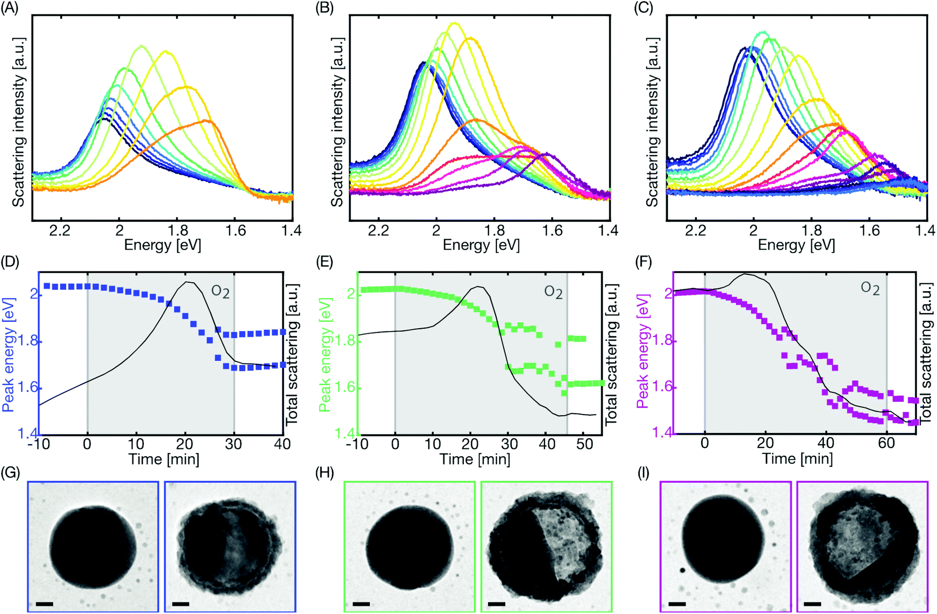 | ||
| Fig. 2 Single particle optical response during oxidation. The optical scattering spectra collected from three individual Cu nanoparticles during (A) 30 minutes, (B) 45 minutes and (C) 60 minutes oxidation, respectively, all in 1% O2 at 150 °C. Spectra taken every 200 seconds are plotted for each nanoparticle to show their evolution over time as oxidation progresses. Note the reversed energy scale on the x-axis. (D–F) The peak energy (left axis) and the integrated peak intensity (right axis) of the scattering spectra of the same three nanoparticles plotted every 100 seconds. The grey shaded area indicates the 1% O2 interval lasting 30 min, 45 min or 60 min, respectively. After approximately 25 minutes oxidation, the peak splits into two modes for all three nanoparticles, which can be seen also in (A–C). (G–I) TEM images of the same three nanoparticles taken before (left) and after oxidation (right). Scale bars are 20 nm. | ||
As the last step, after completed oxidation and cooling of the sample back to room temperature under Ar flow, we again imaged the particles by TEM to reveal their post-oxidation structure (Fig. 2g–i). This analysis reveals the formation of a homogeneous oxide shell during the first stage of oxidation, followed by the appearance and growth of a Kirkendall void. This void formation is the consequence of the faster diffusion of Cu ions through the oxide compared to oxygen ion diffusion.3 For the extreme case of no inward diffusion of oxygen ions, this scenario will result in a void of the same size as the initial Cu particle. However, since in reality both outward Cu-ion and inward O-ion diffusion occur, the formed void is typically slightly smaller than the original nanoparticle,23 as we also observe in our case.
As the next step of our treatment, we now set out to develop a mechanistic picture of the oxidation process, which we then utilize as the basis for detailed Finite-Difference Time-Domain (FDTD) simulations of the expected single particle optical response. To do this, we first consider Cu nanoparticles in the reduced metallic state (Fig. 3a), during initial oxide shell growth (Fig. 3b), after a void has formed (Fig. 3c) and at almost complete oxidation (Fig. 3d) in 1% O2 in Ar carrier gas at 150 °C. Evidently from the TEM images, up until almost 30 min the oxidation is characterized by a homogeneously growing oxide shell, which is formed by Cu-ions that diffuse from the metallic Cu core to the oxide-gas interface, and that leave Cu-vacancies behind in the core (Fig. 3b). Mechanistically, at a critical estimated vacancy cluster size of 4 vacancies,7 they will start to coalesce to form a larger void. Globally, this process is nicely captured in our TEM images taken at the later oxidation stage, which show the formation of a large void with a straight boundary towards the shrinking metallic core (Fig. 3c and d). However, the resolution is not high enough to enable identification of vacancies and vacancy clusters. Therefore, we speculate that vacancies either are spread out homogeneously over the entire Cu core or that they are localized at the metal–oxide interface. To this end, there are recent studies on Cu nanowires,6,7 which indicate that vacancies are formed all along the metal–oxide interface and then accumulate at grain boundaries, where voids start to grow. The latter is a consequence of the importance of vacancy sinks and a high vacancy generation rate to enable void nucleation, since the void nucleation barrier of Cu is low (2 eV). These conditions are readily fulfilled at surfaces with high atomic step density and at grain boundaries.7 Since we cannot identify grain boundaries in our particles, we assume that vacancy generation and accumulation takes place at the metal–oxide interface.
 | ||
| Fig. 3 TEM images taken at four stages during oxidation and corresponding mechanistic oxidation model. The stages are described as (A) reduced Cu, (B) oxide shell growth, (C) Kirkendall void formation and (D) void growth. Scale bars are 20 nm. To the right of each TEM image (E–G), the corresponding model geometries used to analytically estimate the oxide and void volumes used for calculating the oxidation fraction δ, are depicted. | ||
Based on the sequence of TEM images along the oxidation coordinate displayed in Fig. 3a–d, we can now apply an analytical mechanistic model for the oxidation of a cylindrical Cu nanoparticle to mimic the shape of the nanodisks used in the experiment (Fig. 3e–h). Specifically, we adopt the theoretical model developed by Susman et al.23 in the NKE limit, where it is assumed that exclusively Cu-ion outward diffusion is responsible for the oxide shell growth. This assumption is reasonable due to the known higher diffusion rate of Cu-ions compared to O-ions in Cu2O,3 and also corroborated specifically for the case at hand by the observation that the void inner diameter of particles oxidized for 30 minutes is maximally 9%, and correspondingly after 60 minutes of oxidation 11%, smaller than the initial metallic particle (Fig. S3†). In this model, the thickness of the oxide shell is calculated as the difference between the radius of the annealed particle a0 and the oxidized particle a1. Since we assume that the core does not shrink, tshell = a1 − a0.
In the NKE limit, the initial Cu core volume V0 is after complete oxidation converted into an oxide shell with volume Vox,final = ZV0. Futhermore, as we assume no core contraction, the oxide volume at any stage during the oxidation can be calculated as
| Vox = πa12(h + tshell) − πa02h | (1) |
Resorting to a large set of TEM images obtained for sample sets comprising a total of 38 single Cu nanoparticles each, and oxidized for 30 min (s1), 45 min (s2) or 60 min (s3), respectively in 1% O2 in Ar carrier gas at 150 °C, we can extract the corresponding oxide shell thickness, tshell and oxidation fraction, δ, for each nanoparticle from the experiment and plot them against each other (Fig. 4a). Comparing the experimental data points with the calculated oxide shell growth range for disk-shaped particles with diameters ranging between 95 to 105 nm based on eqn (1) reveals excellent agreement and thus corroborates our approach.
 | ||
| Fig. 4 Measured oxide shell thickness. (A) The oxide shell thicknesses have been derived from TEM images of Cu nanoparticles oxidized for either 30 min (s1p1,2,3), 45 min (s2p1,2,3) or 60 min (s3p1,2,3). 3 particles from each sample have been named and marked by color-coded squares corresponding to the TEM images in (B). The rest of the particles analyzed from the same samples are represented as black circles. The grey shaded area is the calculated oxide shell growth range for disk shaped particles with diameters ranging between 95 to 105 nm, as obtained using eqn (1). Inset: The disk model for calculating the oxide thickness and void volume. (B) TEM images obtained in the reduced state before oxidation (left) and sequentially after the oxidation (right) of the same 9 color-coded particles as in (A). The scale bars are 20 nm. | ||
From these data we also immediately see that the oxidation fraction after 30 min of oxidation (s1p1–3), when the Kirkendall voids just about start to form, is approximately δ = 0.3–0.4, in good agreement with a recent experimental ensemble study.4 Therefore, we define the threshold for also including void nucleation and growth in the model as δ = 0.3, which translates into an oxide shell thickness of tshell = 7 nm. For the second stage of the oxidation including the NKE, the volume of the growing void Vvoid can be calculated using the following expression
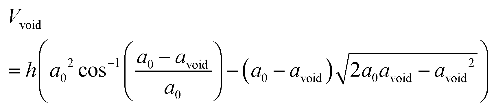 | (2) |
For the next step of our analysis, we developed an FDTD model based on the mechanistic analytical model developed and benchmarked above, to be able to connect the experimentally in situ measured evolution of single particle scattering spectra during oxidation to the mechanistic details of the different oxidation regimes. Specifically, in this FDTD model, the initial metallic Cu disk has a radius a0 = 50 nm and a height of h = 40 nm with slightly rounded corners with a curvature of 5 nm (Fig. 5d). Furthermore, we used eqn (2) to calculate the size of the Kirkendall void for a specific oxidation fraction δ, for which we then simulated the corresponding scattering spectra using FDTD.
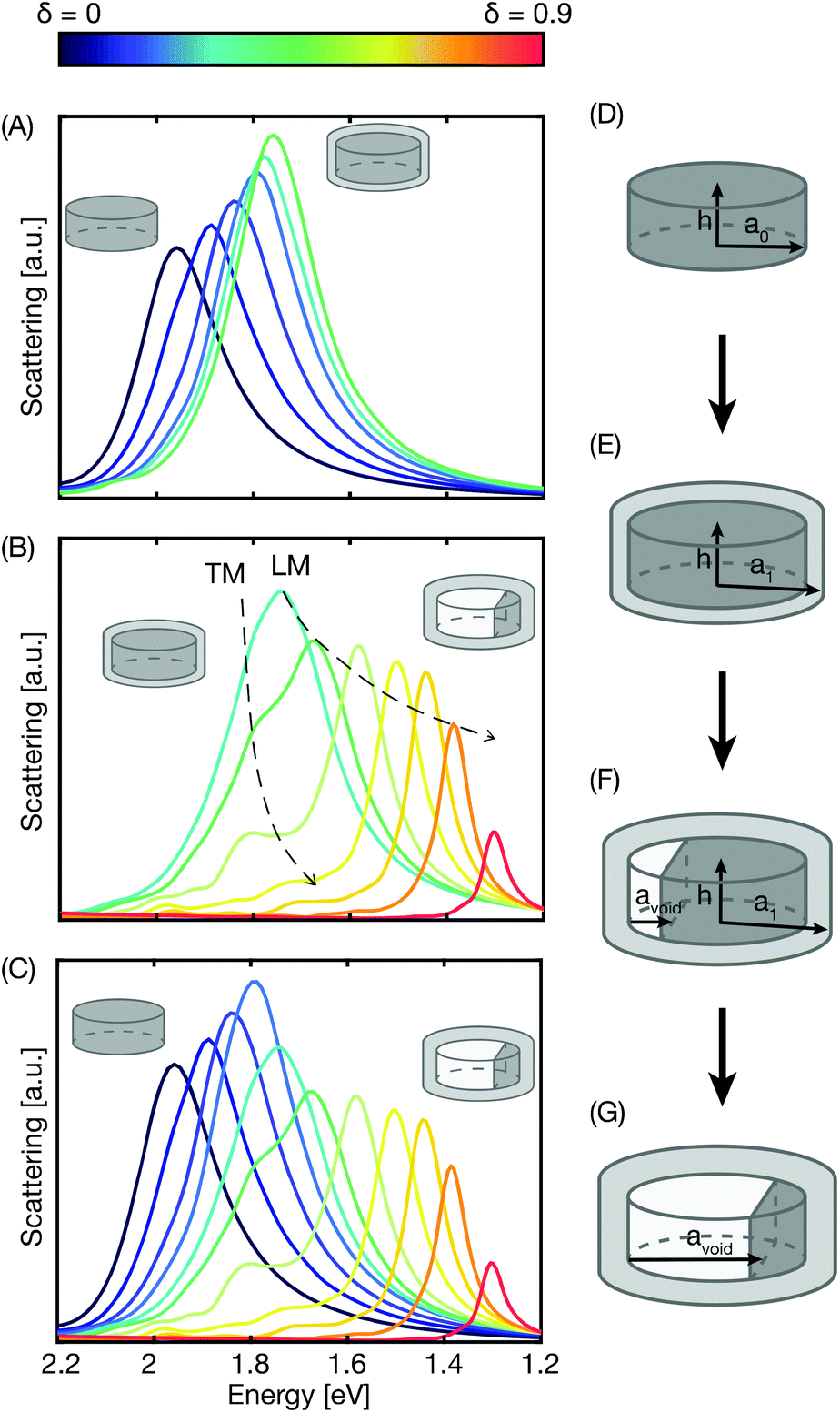 | ||
| Fig. 5 FDTD simulations of the single Cu nanoparticle oxidation process. (A) The first stage of a growing oxide shell simulated with shells ranging in thickness from 0 to 8 nm for an unpolarized incoming plane wave. The core is a solid Cu disk, 100 nm in diameter, 40 nm high with rounded corners with a bending radius of 5 nm. Note that the peak red shifts and increases in intensity due to increased RI of the surrounding as the oxide grows. (B) The second stage of single Cu nanoparticle oxidation, the Kirkendall void formation, simulated by increasing the void volume in concert with the oxide shell volume growth (calculated from the model depicted in Fig. 3). The void growth starts at δ = 0.3. Note that two modes appear, TM perpendicular to the void/metal interface, and LM parallel to the interface. (C) Combining the simulations from (A) up to δ = 0.3 with the ones in (B) after the change of mechanism yields the complete evolution of the scattering spectrum from δ = 0 up to 0.9 for a single Cu nanodisk during oxidation. Qualitatively, it agrees well with the corresponding single nanoparticle experiments depicted in Fig. 2. The insets in (A–C) depicts the start and end geometries for each simulation series. The schematics of the oxide shell growth and sequential void formation and growth are visualized in (D–G) and can be described as (D) reduced Cu disk, (E) oxide shell growth, (F) Kirkendall void formation defined to start at δ = 0.3 and (G) void growth. | ||
Using this model, we first simulated the initial stage of oxidation when homogeneous growth of the oxide layer takes place. This gives rise to a shift of the resonance peak to lower photon energies and to an increase in the scattering intensity due to the higher refractive index of the formed Cu2O (Fig. 5a), in very good agreement with the experiment (cf.Fig. 2). We also note that during this initial stage, the vacancy density in the Cu core is expected to increase, which in turn leads to a reduction of the free electron density. Trying to take this effect into account by Maxwell–Garnett mixing of the dielectric function of Cu with vacuum up to 30% vacancy density, we find that the effect only induces a further red-shift of the peak and a slight increase of the scattering intensity, while no other changes are apparent in the scattering response (Fig. S6†). Hence, from here forward, we have chosen not to include this effect in our simulations to reduce the complexity of the model.
As the oxidation then advances to the second stage, a void nucleates and grows in size, while simultaneously the oxide shell keeps thickening (Fig. 5b). For the subsequently simulated steps, the volume of the oxide shell formed during the second stage equals that of the void times the expansion factor Z. As the void grows in size, the metallic Cu core volume shrinks and at the same time the aspect ratio (AR) of the core changes from a disk with AR = 1 to a semicircular shape (Fig. 5f and g). As the simulations show, the shrinking of the core decreases the scattering intensity of the plasmon resonance, which counteracts the simultaneously increasing scattering caused by the oxide shell growth. More or less simultaneously, we observe the first indication of a “shoulder” riding on the high-energy side of the scattering peak, which becomes more pronounced as the void grows and spectrally induces the distinct peak split. This effect can be explained by the change in AR of the metallic core as the void volume increases, since the developing semicircular shape is no longer centrosymmetric and thus exhibits two in-plane plasmon modes, i.e., a longitudinal mode (LM) and a transversal mode (TM). Specifically, as the void volume increases, the AR of the remaining Cu core increases (AR > 1), giving rise to a longitudinal mode at lower photon energies that is excited in parallel with the void–metal core interface, and a transversal mode at higher photon energies perpendicular to the void–core interface.
A selection of calculated spectra for unpolarized incident illumination (thus exciting both the LM and TM modes) as they evolve along the oxidation reaction coordinate are plotted in Fig. 5b, and corresponding simulations for nanorods of similar dimensions and increasing AR are shown in Fig. S5† for comparison. Combining the FDTD simulations for both oxidation regimes results in an evolution of the scattering spectra and the corresponding key features (Fig. 5c) that qualitatively agree very well with the experimentally measured in situ response of single Cu nanoparticles (cf.Fig. 2a–c).
This analysis has the following intermediate key consequences: (i) it corroborates the capability of the FDTD simulation tool to accurately model the optical response of individual Cu nanoparticle oxidation, including the NKE; (ii) it suggests that the appearance of a characteristic peak split in the single particle scattering spectrum signals the onset of the Kirkendall void formation. Hence, using this tool, it becomes possible to quantitatively analyze the oxidation process of individual nanoparticles in situ at the mechanistic level.
Therefore, as the last step of our treatment, we set out to directly compare the FDTD simulation results with our experimental data (Fig. 6). For 10 min oxidation (s0p1–3) in the experiment a homogeneous oxide layer of 3.3 ± 1.2 nm has formed but no void (Fig. S4†), a peak split in the scattering spectrum has not yet occurred and the oxidation fraction δ is well below 0.3 – all in good agreement with the corresponding FDTD simulations for this regime. Then, the three particles oxidized for 30 minutes (s1p1–3) are localized around the oxidation fraction δ = 0.3, where the peak split occurs in the FDTD model due to the introduction of the Kirkendall void formation at δ = 0.3, in agreement with the experimentally observed onset of void formation in particles s1p2 and s1p3 (Fig. 4b), and the corresponding peak split in the experimental single particle spectra (Fig. S7†). For even longer oxidation times (45 and 60 minutes, particles s2p1–3 and s3p1–3, respectively), we find general agreement with the presence of two peaks in the single particle scattering spectra, as well as their spectral red-shift, as predicted from the FDTD simulations for the corresponding oxidation fractions derived from TEM.
 | ||
| Fig. 6 Comparison of experimental single particle data with corresponding FDTD simulations. The spectral position of the single or double (split) scattering peak(s) obtained from the FDTD model is plotted (on the right y-axis) as a function of oxidation fraction in steps of δ = 0.1 (black circles). Also plotted (color-coded triangles on the left y-axis) are experimental data for single particles before and after 10 min (s0p1–3), 30 min (s1p1–3), 45 min (s2p1–3) and 60 min (s3p1–3) of oxidation, respectively. Note that the y-axes are shifted by 0.1 eV to each other due to the offset in the peak energy from FDTD model. Evidently, the FDTD simulations reproduce the single-peak response of the 10 min oxidation sample (s0). Furthermore, the Kirkendall void formation introduced in the FDTD model at δ = 0.3 is in agreement with the peak split in the scattering resonance observed for sample s1, oxidized for 30 minutes and the spectral evolution (red-shift) of the two peaks during Kirkendall void growth, as seen for the samples oxidized for 45 and 60 minutes (s2 and s3), is also correctly reproduced. The solid grey line is a guide to the eye for the trend of the FDTD data, highlighting the peak split due to the Kirkendall void formation at δ = 0.3. The disk models used in the FDTD simulations are added at the different stages during oxidation to visualize the approximate oxidation fraction δ. | ||
Conclusions
In summary, we have developed a combined experimental and theoretical platform for the investigation of single Cu nanoparticle oxidation. Specifically, this is enabled by combining in situ single particle plasmonic nanospectroscopy with post mortem TEM imaging for comparison of the final structure with the single particle optical response. Using a detailed mechanistic FDTD model of the oxidation process, we furthermore were able to show that the characteristic features observed in the experimental single particle scattering spectra evolution along the reaction coordinate can be related to different oxidation regimes and the corresponding oxidation mechanism. For example, the initial homogeneous growth of an oxide shell gives rise to a spectral red-shift, as well as distinct increase in scattering intensity. The transition to a second oxidation regime beyond a critical oxide thickness of 7 nm is then signaled by a distinct split of the LSPR peak into two modes. They are the consequence of the onset of Kirkendall void formation and the corresponding loss of the centrosymmetric geometry of the metallic core. Hence, we find that this split of the scattering resonance can be generally interpreted as the signal for the onset of Kirkendall void formation in metal nanoparticles, and that it occurs at an oxidation fraction of δ = 0.3 for the Cu nanoparticles studied here.In a wider perspective, this work presents the foundation for the application of single particle plasmonic nanospectroscopy in investigations of the impact of parameters like particle size, shape and nanostructure with respect to defects and grain boundaries on the oxidation of metal nanoparticles. Furthermore, it may also enable structure–function correlations at the single nanoparticle level in metal nanoparticle alloy formation or in heterogeneous catalysis applications by, for example, enabling the operando identification of the active phase at the single nanoparticle level during a catalytic reaction.27
Experimental
In situ dark-field nanospectroscopy
The in situ oxidation measurements were carried out in a Linkam reaction cell (THMS600), with optical access, which was mounted on an upright Nikon Eclipse LV150 N microscope. The reactor cell was connected to mass flow controllers (Bronkhorst, low-ΔP-flow) to regulate the supplied gas mixture at atmospheric pressure. The gases used were 100% Ar (6.0 purity) mixed with either 15% (±2 rel.%) O2 in Ar to achieve 1% O2 in total, or mixed with 100% H2 to achieve 4% in total concentration. The microscope is equipped with a dark field objective (Nikon TU plan ELWD 50×, NA = 0.60, WD = 11 mm) and spectroscopic analysis was enabled by an Andor Shamrock SR-193i (grating blaze 800 nm, density 149 l mm−1) and an Andor Newton 920 CCD camera (256 × 1024 pixels). The imaged particles were aligned in columns separated by 10 μm, and each row of particles was separated by 7 μm, to allow for the background scattering being collected around each particle. The single particle scattering spectra were then calculated as Isc(λ) = (S − B)/CRS, where S is the signal collected from a box defined around the nanoparticle, B is the background scattering measured on the CCD chip both above and below the nanoparticle, defined as B = Babove + Bbelow and CRS is the spectrum of the 50 W halogen lamp collected from a diffuse white certified reflectance standard bright reference sample (Labsphere SRS-99-020). The data was collected in image-mode, meaning that the spectral coordinate was on the x-axis and the spatial coordinate along the slit opening, on the y-axis. The image-mode data collection enables post-particle tracking in one-dimension, as well as post configuring of data boxes for each nanoparticle for the extraction of relevant data. For the kinetic series, typically a spectrum was collected every 10 s. For data analysis, 10 spectra of 10 sequential data points were averaged to increase signal/noise. Then, the averaged spectra were analyzed by fitting either one or two Lorentzian functions based on the criterion that, if the R2 of the fit of one Lorentzian was lower than 95%, the best fit of either one or two Lorentzian peaks were used. To this end, “best” meaning that two peaks had to yield a 1 or 2% improvement of the fit, depending on the data quality.Sample fabrication
The procedure for fabricating arrays of Cu nanoparticles was: (i) Spin coating copolymer MMA(8.5)MMA (MicroChem Corporation, 10 wt% diluted in anisole) at 6000 rpm for 60 s and soft baking at 180 °C for 5 min on a hotplate. Spin coating PMMA A2 at 3000 rpm for 60 s and soft baking at 180 °C for 5 min on a hotplate. (ii) Electron-beam exposure at 2 nA with a shot pitch of 2 nm and a 2000 μC cm−2 exposure dose (JEOL JBX 9300FS). (iii) Development in methyl isobutyl ketone(MIBK)![[thin space (1/6-em)]](https://www.rsc.org/images/entities/char_2009.gif) :isopropanol (1:3) for 120 s, rinsing in isopropanol and drying under N2-stream. (iv) Electron-beam evaporation (Lesker PVD 225) of 40 nm Cu at a rate of 1–2 Å s−1 followed by lift-off in acetone and drying under N2-stream. (v) Annealing in 4% H2 in Ar at 400 °C for 24 h, to yield the low grain density microstructure. The nanoparticles were fabricated on a 25 nm thin SiNx membrane of size 120 × 120 μm wide, made according to ref. 25.
:isopropanol (1:3) for 120 s, rinsing in isopropanol and drying under N2-stream. (iv) Electron-beam evaporation (Lesker PVD 225) of 40 nm Cu at a rate of 1–2 Å s−1 followed by lift-off in acetone and drying under N2-stream. (v) Annealing in 4% H2 in Ar at 400 °C for 24 h, to yield the low grain density microstructure. The nanoparticles were fabricated on a 25 nm thin SiNx membrane of size 120 × 120 μm wide, made according to ref. 25.
Finite-difference time-domain simulations
The FDTD simulations were performed using the commercial software FDTD Solutions (Lumerical), the Cu disk had a radius of 50 nm and a height of 40 nm. The edges were rounded with a curvature of 5 nm. The steps of the growth of the shell and void were calculated numerically according to eqn (1) and (2). The dielectric functions for Cu and Cu2O were taken from McPeak28 and Tahir,29 respectively. The void was simulated as vacuum (RI = 1). The substrate was a 25 nm thin Si3N4 film, with dielectric data from Philipp,30 where the RI is approximately 2. The incoming electrical field was simulated as a plane wave polarized along one of the axes in the Cu core using a total-field/scattered-field source. Furthermore, the scattering cross-section was obtained by integrating the Poynting vector of the scattered field and summing the scattering cross-sections obtained from the two perpendicular polarizations.Transmission electron microscopy
The particles were imaged before and after in situ oxidation measurements in a FEI Tecnai T20 (LaB6 filament, operated at 200 kV). For decreasing the hydrocarbon polymer deposition from the beam during imaging, the sample was taken directly after annealing at 400 °C in 4% H2/96% Ar mixture in the reaction cell to the TEM, as well as the particles were imaged only for 10–20 s. Imaging was done in bright field-mode at 43k× magnification with a dose rate of 4000–6000 e nm−2 s−1. An objective aperture was inserted to remove ghost images from the diffraction in the crystal planes of the particles.Author contributions
The manuscript was written through contributions of all authors. All authors have given approval to the final version of the manuscript.Conflicts of interest
There are no conflicts to declare.Acknowledgements
This research has received funding from the European Research Council (ERC) under the European Union's Horizon 2020 research and innovation programme (678941/SINCAT) and from the Knut and Alice Wallenberg Foundation project 2015.0055. We also thank the Knut and Alice Wallenberg Foundation for their support of the infrastructure in the MC2 nanofabrication laboratory at Chalmers. TJA thanks the Polish National Science Center for support via the project 2017/25/B/ST3/00744. Part of this work was carried out at the MC2 cleanroom facility and at the Chalmers Materials Analysis Laboratory.Notes and references
- W. Wang, M. Dahl and Y. Yin, Hollow Nanocrystals through the Nanoscale Kirkendall Effect, Chem. Mater., 2013, 25, 1179–1189 CrossRef CAS.
- Y. Yin, R. M. Rioux, C. K. Erdonmez, S. Hughes, G. A. Somorjai and A. P. Alivisatos, Formation of Hollow Nanocrystals Through the Nanoscale Kirkendall Effect, Science, 2004, 304, 711–714 CrossRef CAS PubMed.
- R. Nakamura, D. Tokozakura, H. Nakajima, J.-G. Lee and H. Mori, Hollow oxide formation by oxidation of Al and Cu nanoparticles, J. Appl. Phys., 2007, 101, 074303 CrossRef.
- M. D. Susman, Y. Feldman, T. A. Bendikov, A. Vaskevich and I. Rubinstein, Real-time plasmon spectroscopy study of the solid-state oxidation and Kirkendall void formation in copper nanoparticles, Nanoscale, 2017, 9, 12573–12589 RSC.
- K. P. Rice, A. S. Paterson and M. P. Stoykovich, Nanoscale Kirkendall Effect and Oxidation Kinetics in Copper Nanocrystals Characterized by Real-Time, In Situ Optical Spectroscopy, Part. Part. Syst. Charact., 2015, 32, 373–380 CrossRef CAS.
- A.-A. El Mel, M. Buffière, P.-Y. Tessier, S. Konstantinidis, W. Xu, K. Du, I. Wathuthanthri, C.-H. Choi, C. Bittencourt and R. Snyders, Highly ordered hollow oxide nanostructures: the Kirkendall effect at the nanoscale., Small, 2013, 9, 2838–2843 CrossRef CAS PubMed.
- C.-L. Huang, W.-L. Weng, C.-N. Liao and K. N. Tu, Suppression of interdiffusion-induced voiding in oxidation of copper nanowires with twin-modified surface, Nat. Commun., 2018, 9, 340 CrossRef PubMed.
- Z. Yang, N. Yang and M.-P. Pileni, Nano Kirkendall Effect Related to Nanocrystallinity of Metal Nanocrystals: Influence of the Outward and Inward Atomic Diffusion on the Final Nanoparticle Structure, J. Phys. Chem. C, 2015, 119, 22249–22260 CrossRef CAS.
- A. P. LaGrow, M. R. Ward, D. C. Lloyd, P. L. Gai and E. D. Boyes, Visualizing the Cu/Cu2O Interface Transition in Nanoparticles with Environmental Scanning Transmission Electron Microscopy, J. Am. Chem. Soc., 2017, 139, 179–185 CrossRef CAS PubMed.
- D. Zhang, C. Jin, Z. Y. Li, Z. Zhang and J. Li, Oxidation behavior of cobalt nanoparticles studied by in situ environmental transmission electron microscopy, Sci. Bull., 2017, 62, 775–778 CrossRef CAS.
- X. He, Y. Wang, X. Zhang, M. Dong, G. Wang, B. Zhang, Y. Niu, S. Yao, X. He and H. Liu, Controllable in Situ Surface Restructuring of Cu Catalysts and Remarkable Enhancement of Their Catalytic Activity, ACS Catal., 2019, 9, 2213–2221 CrossRef CAS.
- A.-A. El Mel, L. Molina-Luna, M. Buffière, P.-Y. Tessier, K. Du, C.-H. Choi, H.-J. Kleebe, S. Konstantinidis, C. Bittencourt and R. Snyders, Electron Beam Nanosculpting of Kirkendall Oxide Nanochannels, ACS Nano, 2014, 8, 1854–1861 CrossRef CAS PubMed.
- A. L. Koh, K. Bao, I. Khan, W. E. Smith, G. Kothleitner, P. Nordlander, S. A. Maier and D. W. McComb, Electron Energy-Loss Spectroscopy (EELS) of Surface Plasmons in Single Silver Nanoparticles and Dimers: Influence of Beam Damage and Mapping of Dark Modes, ACS Nano, 2009, 3, 3015–3022 CrossRef CAS PubMed.
- J. Li and C. Liu, Carbon-coated copper nanoparticles: synthesis, characterization and optical properties, New J. Chem., 2009, 33, 1474 RSC.
- C.-H. Chen, T. Yamaguchi, A. Ko-ichi Sugawara and K. Koga, Role of Stress in the Self-Limiting Oxidation of Copper Nanoparticles, J. Phys. Chem. B, 2005, 109, 20669–20672 CrossRef CAS PubMed.
- D. B. Pedersen, S. Wang and S. H. Liang, Charge-Transfer-Driven Diffusion Processes in Cu@Cu-Oxide Core–Shell Nanoparticles: Oxidation of 3.0 ±0.3 nm Diameter Copper Nanoparticles, J. Phys. Chem. C, 2008, 112, 8819–8826 CrossRef CAS.
- A. Yabuki and S. Tanaka, Oxidation behavior of copper nanoparticles at low temperature, Mater. Res. Bull., 2011, 46, 2323–2327 CrossRef CAS.
- M. Mansour, L. Favergeon and M. Pijolat, Kinetic modeling of low temperature oxidation of copper nanoparticles by O2, Thermochim. Acta, 2013, 570, 41–50 CrossRef CAS.
- D. Albinsson, S. Nilsson, T. J. Antosiewicz, V. P. Zhdanov and C. Langhammer, Heterodimers for in Situ Plasmonic Spectroscopy: Cu Nanoparticle Oxidation Kinetics, Kirkendall Effect, and Compensation in the Arrhenius Parameters, J. Phys. Chem. C, 2019, 123, 6284–6293 CrossRef CAS PubMed.
- L. X. Qin, C. Jing, Y. Li, D. W. Li and Y. T. Long, Real-time monitoring of the aging of single plasmonic copper nanoparticles, Chem. Commun., 2012, 48, 1511–1513 RSC.
- S. Alekseeva, A. B. da S. Fanta, B. Iandolo, T. J. Antosiewicz, F. A. A. Nugroho, J. B. Wagner, A. Burrows, V. P. Zhdanov and C. Langhammer, Grain boundary mediated hydriding phase transformations in individual polycrystalline metal nanoparticles, Nat. Commun., 2017, 8, 1084 CrossRef PubMed.
- G. H. Chan, J. Zhao, E. M. Hicks, G. C. Schatz and R. P. Van Duyne, Plasmonic Properties of Copper Nanoparticles Fabricated by Nanosphere Lithography, Nano Lett., 2007, 7, 1947–1952 CrossRef CAS.
- M. D. Susman, A. Vaskevich and I. Rubinstein, A General Kinetic-Optical Model for Solid-State Reactions Involving the Nano Kirkendall Effect. The Case of Copper Nanoparticle Oxidation, J. Phys. Chem. C, 2016, 120, 16140–16152 CrossRef CAS.
- A. A. El Mel, R. Nakamura and C. Bittencourt, Beilstein J. Nanotechnol., 2015, 6 Search PubMed.
- A. W. Grant, Q.-H. Hu and B. Kasemo, Transmission electron microscopy windows for nanofabricated structures, Nanotechnology, 2004, 15, 1175–1181 CrossRef CAS.
- M. Yin, C.-K. Wu, Y. Lou, C. Burda, J. T. Koberstein, Y. Zhu and S. O'Brien, Copper Oxide Nanocrystals, J. Am. Chem. Soc., 2005, 127, 9506–9511 CrossRef CAS PubMed.
- S. Liu, A. S. Arce, S. Nilsson, D. Albinsson, L. Hellberg, S. Alekseeva and C. Langhammer, In Situ Plasmonic Nanospectroscopy of the CO Oxidation Reaction over Single Pt Nanoparticles, ACS Nano, 2019, 13, 6090–6100 CrossRef CAS PubMed.
- K. M. McPeak, S. V. Jayanti, S. J. P. Kress, S. Meyer, S. Iotti, A. Rossinelli and D. J. Norris, Plasmonic Films Can Easily Be Better: Rules and Recipes, ACS Photonics, 2015, 2, 326–333 CrossRef CAS PubMed.
- D. Tahir and S. Tougaard, Electronic and optical properties of Cu, CuO and Cu2O studied by electron spectroscopy, J. Phys.: Condens. Matter, 2012, 24, 175002 CrossRef PubMed.
- H. R. Philipp, Optical Properties of Silicon Nitride, J. Electrochem. Soc., 1973, 120, 295 CrossRef CAS.
Footnote |
| † Electronic supplementary information (ESI) available. See DOI: 10.1039/c9nr07681f |
| This journal is © The Royal Society of Chemistry 2019 |