
 Open Access Article
 This Open Access Article is licensed under a Creative Commons Attribution-Non Commercial 3.0 Unported Licence
Phase-field investigation of the stages in radial growth of core–shell Ge/Ge1−xSnx nanowires†
Yanming
Wang
 *a,
Andrew C.
Meng
b,
Paul C.
McIntyre
b and
Wei
Cai
*c
*a,
Andrew C.
Meng
b,
Paul C.
McIntyre
b and
Wei
Cai
*c
aDepartment of Materials Science and Engineering, Massachusetts Institute of Technology, Cambridge, MA, USA. E-mail: yanmingw@mit.edu
bDepartment of Materials Science and Engineering, Stanford University, Stanford, CA, USA
cDepartment of Mechanical Engineering, Stanford University, Stanford, CA, USA. E-mail: caiwei@stanford.edu
First published on 1st November 2019
Abstract
Core–shell Ge/Ge1−xSnx nanowires are considered promising silicon-compatible nanomaterials with the potential to achieve a direct band-gap for optoelectronic applications. In this study, we systematically investigated the formation of this heterostructure in the radial direction by the phase field method coupled with elasticity. Our model simulated the shell growth of the wire, capturing the evolution of both the sidewall morphology and the strain distribution. We predicted the minimum chemical potential driving forces required for initiating the Ge1−xSnx shell growth at given tin concentrations. In addition, we studied the dependences of the shell growth rate on the chemical potential, the tin concentration, the sidewall interface kinetics and the mass transport rate respectively. From these analyses, we identified three sequential stages of the growth: the Stage 1 growth at an accelerated rate, the Stage 2 growth at a constant rate, and finally the Stage 3 growth at a reduced rate scaling with  . This research improves our current understanding on the growth mechanisms of heterogeneous core–shell nanowires, and provides useful guidelines for optimizing nanowire synthesis pathways.
Introduction
Ge1−xSnx alloys, featuring a band gap adjustable by Sn composition and induced strain, are considered promising semiconductor materials for a wide range of optoelectronic applications compatible with the mainstream Si-based devices.1–7 Core–shell nanowires (NWs) form an important category of nano-structures, as a means to enable hetero-epitaxial growth8,9 and introduce carrier confinement effects.10 Specifically for the Ge–Sn system, the formation of core–shell Ge/Ge1−xSnx NWs (by chemical vapor deposition) provides a plausible solution to obtain defect-free Ge1−xSnx, where a high Sn concentration can be achieved, well beyond its bulk solubility in Ge.11–13 In addition, due to the lattice mismatch between Ge and Ge1−xSnx, a direct band gap condition of the Ge core may be achieved by tensile straining.14To achieve better control over the quality and yield of the core–shell nanowires, a better understanding of the wire growth mechanisms is of great significance. For this purpose, recently several studies have been conducted,15–18 where modeling and simulations were employed to explain the strain distributions across the cross section of the wire. In comparison with these static calculations, modeling the dynamics of the heterogeneous core–shell structure formation should provide new insight and description of the growth process from a different angle, which motivates the work presented in this paper. Here we systematically study the radial growth of core–shell Ge/Ge1−xSnx nanowires, using an improved phase field model coupled with elasticity based on our previous developments.16,19–21 The simulations reasonably capture the evolution of the wire interface morphology and strain distribution during the shell growth process. The model also predicts a tin concentration dependent minimum chemical potential for the growth activation. From a comprehensive investigation on the shell growth rate's dependences on various factors, including the chemical potential, the tin concentration, the sidewall interface kinetics and the mass transport rate, three growth stages are identified: initial growth at accelerating speed, semi-steady state growth at constant speed, and mass transport limited growth at reduced speed. This research sheds new light on the growth mechanisms of core–shell Ge1−xSnx nanowires, and provides useful guidelines for synthesizing wires with desired optoelectronic properties.
Results and discussion
In principle, this phase field model is suitable for 3D simulations, to potentially capture the complex sidewall faceting and capillary instability during the nanowire synthesis process.19 However, limited by the computational resource, in this study all the simulations were carried out in quasi-2D. First, one validation run was performed, to demonstrate the model's capability of capturing both the interfacial and elastic properties of the cross section of the core–shell nanowire. The dimensions of the simulation cell were set to 270 × 270 × 1.8 nm3, and the model parameters were calibrated (listed in Table S1†), such that the time and length scales of the simulation could be directly comparable to the experiments (Fig. 3a). Additionally, one assumption of the model is that the core–shell nanowire forms a coherently strained heterostructure, which can be justified by our experimental observations of the NW cross sections by high-resolution transmission electron microscopy (HRTEM) (Fig. S1†). It should be noted that this assumption may break down when the Sn concentration in the shell is extremely high (e.g. ∼20%). Under this condition, significant inhomogeneity of Sn composition were observed, leading to largely altered wire geometry and surface properties.18 As shown in Fig. 1a, starting with a stress-free [111] Ge nanowire, the Ge1−xSnx alloy with a Sn concentration x = 4.2% was continuously deposited under a constant chemical potential driving force. During the growth, the hexagonal cross sectional shape with clear six {112} side-wall facets, was observed in the simulation, matching the wire geometry observed in the experiments (Fig. S1†).16 It is expected, and also well captured by the model that at a small shell thickness, the Ge1−xSnx shell was strained in compression, while the Ge core was elongated to accommodate the lattice mismatch between them. When the shell grew thick enough, the core became fully strained in tension so that the elastic strain in the core approached the lattice mismatch between Ge and Ge0.958Sn0.042 (≈0.6% according to eqn (S1)†). In contrast, the shell region was almost strain-free, consistent with observations in the literature.15,16 As a comparison, when a core–shell nanowire is grown to the similar size with a larger initial core diameter, its core is expected to be less stretched, while a certain amount of compressive strain may still reside in the shell region (Fig. S2†). Additionally, the phase field simulation provided the distributions of the in-plane strain components (represented in the polar coordinate system) and the elastic energy density, as shown in Fig. 1b, c and d respectively (the distribution of the two in-plane strain invariants I1 and I2 are provided in Fig. S3†). It is predicted that either εrr or εθθ was more concentrated in the core and near the interface region in the shell, exhibiting a radial symmetry around the center of the wire. This also resulted in a very similar distribution of the elastic energy density wel, all in good agreement with the static calculations done by the finite element method.15 Besides, many features (e.g. the symmetries and the signs of the strain components) of the in-plane strain distributions predicted by this set of calculations are likely to be preserved for core–shell nanowires with different core diameters (Fig. S2†).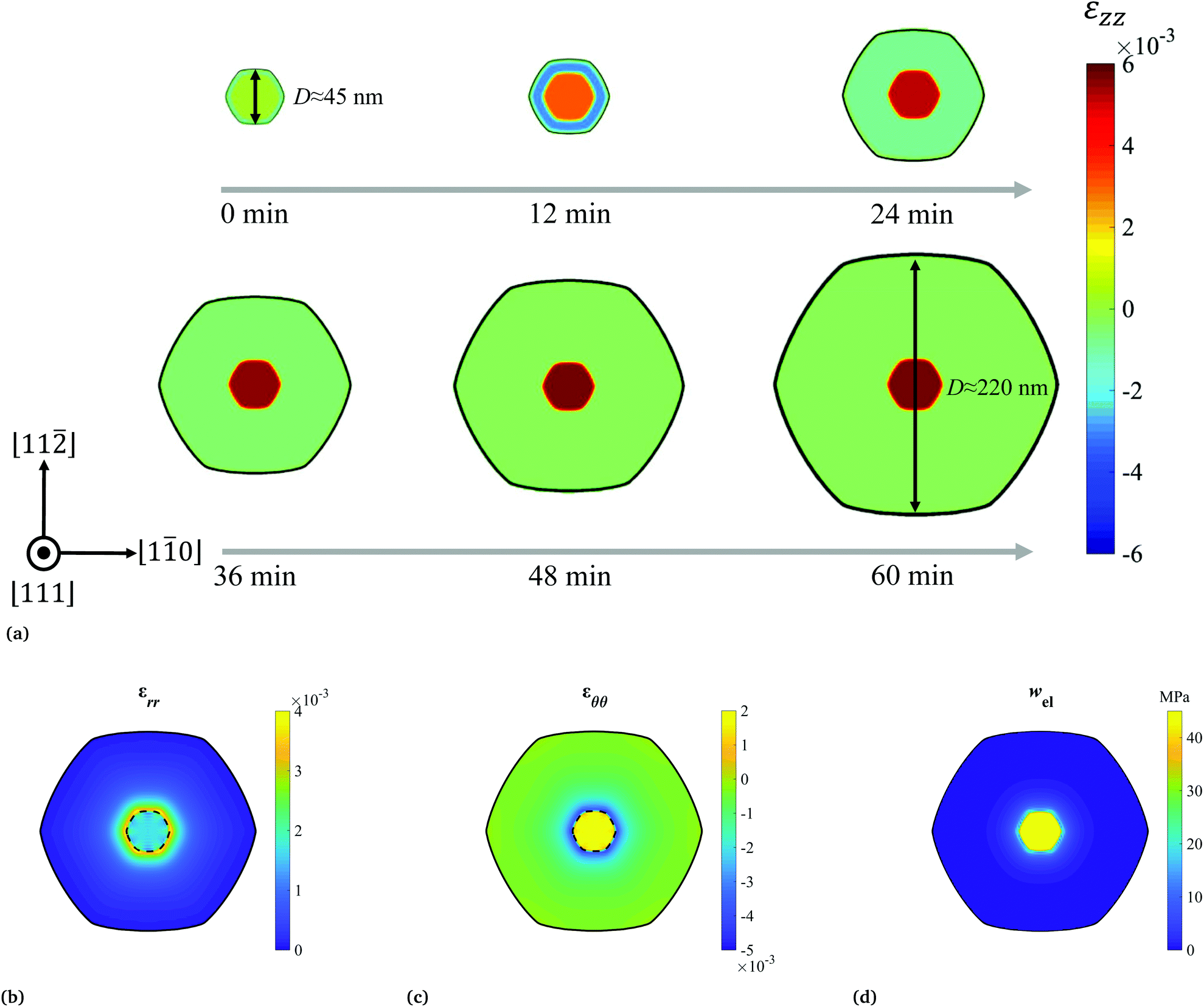 | ||
| Fig. 1 (a) Phase field simulation snapshots show the radial growth of one Ge/Ge0.958Sn0.042 core/shell nanowire, capturing the evolution of the normal strain distribution in the out-of-plane direction. The distributions of the in-plane strain components for the grown nanowire are given by (b) εrr and (c) εθθ. The elastic energy density distribution wel of the nanowire cross section is given in (d). | ||
A series of phase field simulations were performed at different vapor chemical potentials (μV) (the chemical potential in the solid phase is set to 0), keeping the interface kinetic coefficient K at 10 nm3 (eV min)−1 and Sn concentration of the shell (Sn%) at 4.2%. (The values of the kinetic coefficient K and the time step Δt were chosen, to reproduce the experimental NW diameter-growth time relationship shown in Fig. 3.) It should be noted that for practical CVD growth, these quantities (e.g., μV, K and Sn% as mentioned above) are associated with the partial pressures of H2, GeH4 and SnCl4.‡ And they are often coupled, making it very challenging to tune only one parameter at a time in experiments. Thus in this model these parameters are designed to be independently adjustable, to enable the investigation of the dependence of nanowire growth on each individual factor.
In Fig. 2a, the nanowire diameters DNW were estimated from the simulation trajectories, and plotted as functions of time t. Apparently, under the given condition, a minimum μV of 0.34 eV nm−3 was required to activate the shell growth. When a larger chemical potential was applied, after an initial acceleration of the growth rate, the wire would enter a steady state growth period, where DNW increased linearly with growth time. In Fig. 2b, the relationship between the steady state growth rate vgrowth and the chemical potential μV was quantified, exhibiting a clear linear dependence, where vgrowth was estimated from the slope of the DNW–t curve in Fig. 2a. In fact, vgrowth depends on not only the μV but also the amount of Sn incorporated in the shell. As shown in Fig. 2c, keeping the μV at 0.36 eV nm−3, the nanowire radial growth slowed down with increasing Sn concentration, until the growth was not observed at around 10% Sn. This indicates that to achieve core-shell nanowire growth at higher Sn%, a larger chemical potential μminV is needed (which might be achieved in practice by lowering and optimizing the H2 flow). This hypothesis was confirmed in Fig. 2d, where μminV was calculated and plotted, with respect to a series of Sn%. The results show that for coherent sidewall growth (Sn% = 0), there still requires a minimum chemical potential. This is to compete with the increase of the surface free energy, caused by the newly created surface area (this competition is further revealed by decomposing the total free energy, as shown in Fig. S4†). For heterogenous growth (Sn% > 0), the μminV nearly quadratically increases with Sn%, possibly due to the fact that Sn% is almost linearly correlated with the misfit strain εmisfit (as shown in eqn (S1)†), and the elastic energy is proportional to (εmisfit)2, assuming that the system is in the linear elasticity regime. For shell growth starting with larger core diameters, due to the Gibbs–Thomson effect,22 the required minimum chemical potential μminV is smaller for both homogenous (Sn = 0% ) and heterogenous (Sn > 0%) growth (Fig. S5†).
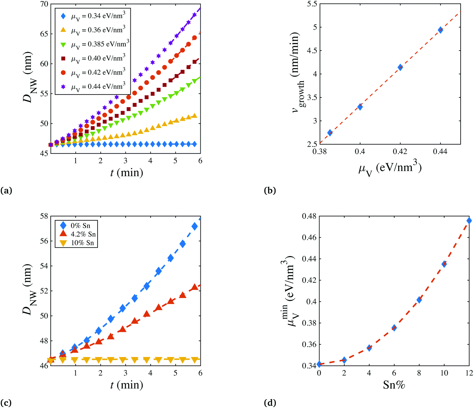 | ||
| Fig. 2 (a) Nanowire diameter (DNW) is plotted as a function of time (t) for shell growth with Sn concentration of 4.2% at various chemical potentials in vapor (μV). The shell growth velocities are extracted from the DNW–t curves and plotted as a function of μV in (b). At a constant μV of 0.36 eV nm−3, DNW is plotted as a function of t at various Sn concentrations in (c). (d) The minimum chemical potential μminV for shell growth is plotted as a function of Sn%. | ||
In the above simulations, the steady stage growth is achieved when the nanowire diameter DNW goes linearly with time t. However, for the experimental results presented in Fig. 3a and b (The SEM images of the grown wires taken at different times are provided in Fig. S6.†), from t ≈30 min till the end of the growth, the wire diameter DNW is found to be scaled with  instead of t. We think that in this case, it is the mass transport, rather than the chemical potential driving force, that dominates the GeSn growth. To corroborate this hypothesis, phase field simulations were performed, with introducing the control of a maximum volumetric material conversion rate vmaxvol. (The implementation of the vmaxvol control is given in eqn (2), with more discussions on its interpretation provided in the ESI.†) As shown in Fig. 3a, at vmaxvol = 25.1 nm3 s−1, the model predicted an identical DNW–t relationship to the experiments, while when vmaxvol was increased to 100 nm3 s−1, DNW exhibited a linear dependence on t in the “steady state” growth regime, at least up to DNW = 240 nm.
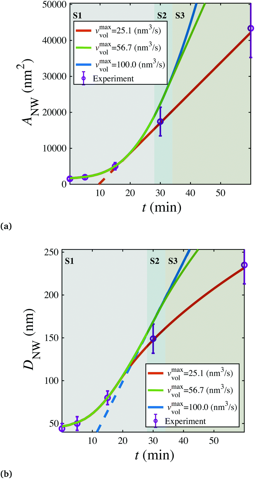 | ||
| Fig. 3 (a) Nanowire cross sectional area (ANW) and (b) diameter (DNW) are plotted as a function of time (t) for shell growth bounded by different maximal mass transport rates, in comparison with experimental data (Fig. S6†). S1, S2, and S3 are the initial, chemical potential limited, and mass-transport limited stages of shell growth, respectively. | ||
It can be expected that ultimately, the shell growth rate should always be bounded by vmaxvol when the wire reaches a certain DNW, as the amount of materials needed to fill a new atomic layer of the shell continuously increases with a larger wire diameter. Therefore, the core–shell nanowire growth can be categorized into three stages (marked as three patches on Fig. 3): Stage 1 (S1), where the radial growth starts and progressively increases, due to the gradual reduction of elastic energy density away from the Ge/GeSn interface; then Stage 2 (S2), where the radial growth rate becomes a constant with its magnitude determined by the vapor chemical potential; and finally Stage 3 (S3), where the nanowire growth is limited by the mass transport process, yielding the growth rate scaling with  .
.
One critical condition for the radial growth of the GeSn alloy is to activate the wire sidewalls by disrupting their hydrogen surface passivation, which in experiments can be associated with reducing the ratio of the H2 partial pressure to the partial pressure of SnCl4.16 In the phase field simulation, this experimental treatment was represented by altering the interface kinetic coefficient K. The effects of K on the wire growth behaviors were examined and summarized in Fig. 4. As shown in Fig. 4a and b, with the shapes of these curves qualitatively preserved at different Ks, the shell growth was significantly accelerated by enlarging K, under adequate supply of precursor materials (e.g. vmaxvol = 100 nm3 s−1). Quantitatively, as shown in Fig. 4c, the total time of the wire in the initial Stage 1 growth was inversely proportional to K. After the wire entered the Stage 2 growth, its growth velocity vgrowth, extracted from the slope of the DNW–t curve, manifested a linear dependence on K, as plotted in Fig. 4d. Based on our previous discussion, the wires with higher K are expected to enter the Stage 3 growth earlier, but after that, still, vgrowth is expected to solely depend on the vmaxvol.
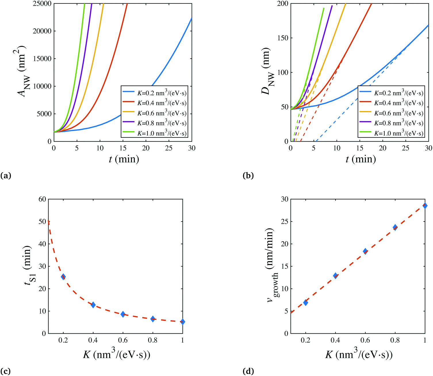 | ||
| Fig. 4 (a) Nanowire cross sectional area (ANW) and (b) diameter (DNW) are plotted as a function of time for a series of interface kinetic coefficient K. (c) The time of growth in Stage 1 is plotted as a function of K. (d) Thenanowire radial growth velocity in Stage 2 is plotted as a function of K. | ||
Conclusion
In this paper, we systematically studied the radial growth of core–shell Ge/Ge1−xSnx nanowires, using a phase field model coupled with elasticity. The model successfully captured several important features of the wire during its growth process, including the sidewall facets and elastic energy distributions. The minimum chemical potentials were predicted for initiating shell growth at given tin concentrations. The effects of chemical potential, interface kinetics, mass transport, and tin concentration on the core–shell nanowire growth were discussed, from which three growth stages were identified. While these findings shed new lights on the mechanisms of core–shell Ge/Ge1−xSnx nanowire growth via the chemical vapor deposition approach, our phase field model provides a useful tool for investigating the synthesis process of a broad range of other heterogeneous materials.Method
Phase field model
In this model, the phase field ϕ(x) and the displacement field u(x) serve as the fundamental degrees of freedom. Then the total free energy of the system can be expressed in the form of a functional in eqn (1) with adopting the Einstein summation convention,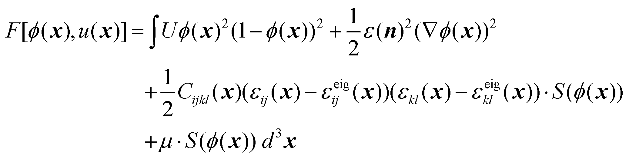 | (1) |
![[thin space (1/6-em)]](https://www.rsc.org/images/entities/char_2009.gif) h(10ϕ − 5) + 1]/2), Cijkl(x) is the stiffness tensor at position x,§εij represents the ij component of the strain tensor calculated from the displacement field u by εij = ½(ui,j + uj,i), and εeigij is a preset eigen-strain field to account for the misfit strain between the nanowire core and shell (eqn (S1)†). The values of the above model parameters are provided in Table S1.†
h(10ϕ − 5) + 1]/2), Cijkl(x) is the stiffness tensor at position x,§εij represents the ij component of the strain tensor calculated from the displacement field u by εij = ½(ui,j + uj,i), and εeigij is a preset eigen-strain field to account for the misfit strain between the nanowire core and shell (eqn (S1)†). The values of the above model parameters are provided in Table S1.†
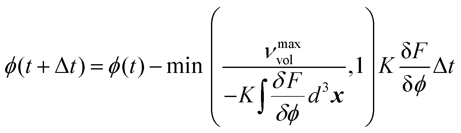
During the simulation, the phase field evolves to reduce the total free energy of the system, governed by the Ginzburg–Landau type equation of motion.23,24 As expressed in eqn (2), the Euler forward time integrator, with modifications to account for the mass transport limit, is adopted to update the phase field ϕ at time t + Δ t based on its value at time t,
 | (2) |
 is the variational derivative of the total free energy F with respect to ϕ (eqn (S3)†), and Δt is the simulation time step. As demonstrated in eqn (3), within each Δt, sub-cycling steps are taken to evolve the displacement field u(x), lowering the total elastic free energy in response to the change of ϕ(x),
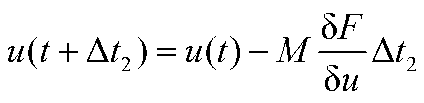 | (3) |
 calculates the variational derivative of F with respect to u (eqn (S4)†).
Experiments
Germanium-tin shells were grown on germanium nanowires grown by gold catalyzed vapor–liquid–solid (VLS) growth similar to previous work.11,16 Ge core nanowires were grown at a total pressure of 30 Torr. The process consisted of a 6 minutes anneal at 375 °C under hydrogen followed by a 4 minutes nucleation step 375 °C under 0.47 Torr GeH4, which was used to initiate Ge nanowires. Steady state growth of Ge nanowires was carried out at 300 °C. GeSn shells of various thicknesses were grown at 300 °C with a SnCl4 partial pressure of 0.022 Torr and a GeH4 partial pressure of 0.47 Torr by varying the growth time from 0 minute to 60 minutes.Conflicts of interest
There are no conflicts to declare.Acknowledgements
Y. W. would like to acknowledge financial support from the Toyota Research Institute. A. C. M. would like to acknowledge funding from NSF GRFP award DGE-114747 and an ARCS Foundation Fellowship. This work is supported by the National Science Foundation Division of Materials Research programs DMR-1608927 and DMR-1206511. Some of the computing work was performed on the Sherlock cluster, provided by the Stanford Research Computing Center. Some of the experimental work was performed at the Stanford Nano Shared Facilities supported by the National Science Foundation under award ECCS-1542152.References
- W. Wegscheider, K. Eberl, U. Menczigar and G. Abstreiter, Appl. Phys. Lett., 1990, 57, 875–877 CrossRef CAS.
- J. Mathews, R. Roucka, J. Xie, S.-Q. Yu, J. Menéndez and J. Kouvetakis, Appl. Phys. Lett., 2009, 95, 133506 CrossRef.
- J. Mathews, R. Beeler, J. Tolle, C. Xu, R. Roucka, J. Kouvetakis and J. Menendez, Appl. Phys. Lett., 2010, 97, 221912 CrossRef.
- S. Su, B. Cheng, C. Xue, W. Wang, Q. Cao, H. Xue, W. Hu, G. Zhang, Y. Zuo and Q. Wang, Opt. Express, 2011, 19, 6400–6405 CrossRef CAS PubMed.
- M. Oehme, J. Werner, M. Gollhofer, M. Schmid, M. Kaschel, E. Kasper and J. Schulze, IEEE Photonics Technol. Lett., 2011, 23, 1751–1753 CAS.
- S. Biswas, J. Doherty, D. Saladukha, Q. Ramasse, D. Majumdar, M. Upmanyu, A. Singha, T. Ochalski, M. A. Morris and J. D. Holmes, Nat. Commun., 2016, 7, 11405 CrossRef CAS PubMed.
- M. Polak, P. Scharoch and R. Kudrawiec, J. Phys. D: Appl. Phys., 2017, 50, 195103 CrossRef.
- L. J. Lauhon, M. S. Gudiksen, D. Wang and C. M. Lieber, Nature, 2002, 420, 57 CrossRef CAS PubMed.
- I. A. Goldthorpe, A. F. Marshall and P. C. McIntyre, Nano Lett., 2008, 8, 4081–4086 CrossRef CAS PubMed.
- B. H. Badada, T. Shi, H. E. Jackson, L. M. Smith, C. Zheng, J. Etheridge, Q. Gao, H. H. Tan and C. Jagadish, Nano Lett., 2015, 15, 7847–7852 CrossRef CAS PubMed.
- A. C. Meng, C. S. Fenrich, M. R. Braun, J. P. McVittie, A. F. Marshall, J. S. Harris and P. C. McIntyre, Nano Lett., 2016, 16, 7521–7529 CrossRef CAS PubMed.
- S. Assali, A. Dijkstra, A. Li, S. Koelling, M. Verheijen, L. Gagliano, N. Von Den Driesch, D. Buca, P. Koenraad and J. Haverkort, et al. , Nano Lett., 2017, 17, 1538–1544 CrossRef CAS PubMed.
- J. Aubin and J. Hartmann, J. Cryst. Growth, 2018, 482, 30–35 CrossRef CAS.
- M. El Kurdi, H. Bertin, E. Martincic, M. De Kersauson, G. Fishman, S. Sauvage, A. Bosseboeuf and P. Boucaud, Appl. Phys. Lett., 2010, 96, 041909 CrossRef.
- M. Albani, S. Assali, M. A. Verheijen, S. Koelling, R. Bergamaschini, F. Pezzoli, E. P. Bakkers and L. Miglio, Nanoscale, 2018, 10, 7250–7256 RSC.
- A. Meng, M. Braun, Y. Wang, C. Fenrich, M. Xue, D. Diercks, B. Gorman, M.-I. Richard, A. Marshall and W. Cai, et al. , Mater. Today Nano, 2019, 5, 100026 CrossRef.
- S. Assali, R. Bergamaschini, E. Scalise, M. A. Verheijen, M. Albani, A. Li, S. Koelling, E. P. Bakkers, F. Montalenti and L. Miglio, arXiv preprint arXiv:1906.11694, 2019.
- S. Assali, M. Albani, R. Bergamaschini, M. A. Verheijen, A. Li, S. Kölling, L. Gagliano, E. P. Bakkers and L. Miglio, Appl. Phys. Lett., 2019, 115, 113102 CrossRef.
- Y. Wang, P. C. McIntyre and W. Cai, Cryst. Growth Des., 2017, 17, 2211–2217 CrossRef CAS.
- R. Ramachandramoorthy, Y. Wang, A. Aghaei, G. Richter, W. Cai and H. D. Espinosa, ACS Nano, 2017, 11, 4768–4776 CrossRef CAS PubMed.
- X. Zhang, Y. Wang and W. Cai, J. Mater. Sci., 2018, 53, 5777–5785 CrossRef CAS.
- D. Kashchiev, Cryst. Growth Des., 2006, 6, 1154–1156 CrossRef CAS.
- P. C. Hohenberg and B. I. Halperin, Rev. Mod. Phys., 1977, 49, 435 CrossRef CAS.
- I. Steinbach and F. Pezzolla, Phys. D, 1999, 134, 385–393 CrossRef.
Footnotes |
| † Electronic supplementary information (ESI) available: Fig. S1, HRTEM image of wire cross sections. Fig. S2, strain distributions of a core–shell nanowire with a larger core diameter. Fig. S3, distributions of the in-plane strain invariants. Fig. S4, free energy decomposition of the nanowire system. Fig. S5, minimum chemical potential driving force as a function of nanowire diameter. Fig. S6, SEM images of Ge/Ge0.958Sn0.042 nanowires. Detailed formulations and parameters (Table S1) of the phase field model. See DOI: 10.1039/C9NR07587A |
| ‡ Increasing the partial pressure of H2 is expected to passivate the surface and suppress the decomposition of GeH4, resulting in the reduction of both μV and K. In contrast, increasing the supply of GeH4 promotes the decomposition of itself, leading to a larger driving force μV for the wire growth. Increasing the partial pressure of SnCl4 brings multiple effects to the system. First, this would naturally increase the Sn concentration of the shell Sn%. Second, Sn, known as a catalyst for Ge growth, activates the nanowire sidewall surface and alter the reaction pathways of Ge incorporation, which enhances K and modifies μV. |
| § In this study, Cijkl is simplified as a constant tensor, considering that the nanowire is a coherent single crystalline material. |
| This journal is © The Royal Society of Chemistry 2019 |