
 Open Access Article
 This Open Access Article is licensed under a
 Creative Commons Attribution 3.0 Unported Licence
Scanning tunneling microscopy and Raman spectroscopy of polymeric sp–sp2 carbon atomic wires synthesized on the Au(111) surface†
Andi
Rabia
 a,
Francesco
Tumino
a,
Alberto
Milani
a,
Valeria
Russo
a,
Andrea
Li Bassi
a,
Simona
Achilli‡
b,
Guido
Fratesi
b,
Giovanni
Onida
b,
Nicola
Manini
b,
Qiang
Sun§
c,
Wei
Xu
c and
Carlo S.
Casari
*a
a,
Francesco
Tumino
a,
Alberto
Milani
a,
Valeria
Russo
a,
Andrea
Li Bassi
a,
Simona
Achilli‡
b,
Guido
Fratesi
b,
Giovanni
Onida
b,
Nicola
Manini
b,
Qiang
Sun§
c,
Wei
Xu
c and
Carlo S.
Casari
*a
aDepartment of Energy, Politecnico di Milano, via Ponzio 34/3, I-20133 Milano, Italy. E-mail: carlo.casari@polimi.it; Tel: +39 0223996331
bETSF and Dipartimento di Fisica, Università degli Studi di Milano, Via Celoria, 16, I-20133 Milano, Italy
cInterdisciplinary Materials Research Center, College of Materials Science and Engineering, Tongji University, Shanghai 201804, P. R. China
First published on 27th September 2019
Abstract
Long linear carbon nanostructures based on sp-hybridization can be synthesized by exploiting on-surface synthesis of halogenated precursors evaporated on Au(111), thus opening a way to investigations by surface-science techniques. By means of an experimental approach combining scanning tunneling microscopy and spectroscopy (STM and STS) with ex situ Raman spectroscopy we investigate the structural, electronic and vibrational properties of polymeric sp–sp2 carbon atomic wires composed by sp-carbon chains connected through phenyl groups. Density-functional-theory (DFT) calculations of the structure and the electronic density of states allow us to simulate STM images and to compute Raman spectra. The comparison of experimental data with DFT simulations unveil the properties and the formation stages as a function of the annealing temperature. Atomic-scale structural information from STM complement the Raman sensitivity to the single molecular bond to open the way to detailed understanding of these novel carbon nanostructures.
1 Introduction
Carbon atomic wires are linear carbon nanostructures based on sp-hybridization, representing the ultimate 1-D carbon system.1,2 For increasing length of the sp-carbon wire these systems approach the ideal carbyne whose predicted outstanding mechanical, electronic and thermal properties make the infinite linear wire an appealing model of 1-D crystal with extended π-electron conjugation.3,4 However, the length of carbon atomic wires has experimentally reached some tens of carbon atoms (up to 42 corresponding to about 5 nm) with sp2 or sp3 carbon terminating molecular groups and up to a few thousands (i.e. exceeding 600 nm) only when encapsulated in a carbon nanotube.5,6 Short carbon atomic wires attract researchers’ attention as well since they exhibit peculiar opto-electronic properties strongly dependent on their length and type of termination, as recently shown in the case of size-selected phenyl-terminated polyynic wires for advanced optical and biosensing applications.7The use of short carbon atomic wires as building units (i.e. oligomers) to form polymeric carbon wires appears as a viable strategy to obtain long linear wires without suffering stability issues. This is particularly true when the polymer is built by using sp-carbon links bridging phenyl groups due to the stability already proven for isolated phenyl-terminated polyynes.8 Such sp–sp2 carbon atomic polymers have been addressed by theoretical calculations showing intriguing properties such as tunable band gap, very high electron mobility and electronic and spin transport sensitive to the wire length and termination capping atoms.9–12 In addition, they represent the smallest nanoribbon or equivalently the 1D building unit of 2D carbon crystals beyond graphene such as graphyne or graphdiyne.13
To this aim, a possible strategy is based on promoting covalent linking (i.e. through polymerization) of suitable molecular precursors on metal surfaces. This on-surface synthesis has been proven for the bottom-up approach of graphene nanoribbons and sp2-carbon systems employing for instance the Ullmann reaction.14–17 The extension of this approach to sp-carbon systems is very recent and rapidly growing.18–25 On-surface synthesis of sp-carbon systems opens a way to scanning-probe microscopy investigations at the molecular level which are otherwise hindered by the difficulties in sample preparation. An early attempt only has shown buckled sp–sp3 chains formed by sublimation of SiC(100)26. On-surface synthesis in combination with scanning-tunneling or atomic-force microscopy (STM/AFM) has been adopted as a playground to direct image and study some sp-carbon based systems ranging from the single acetylenic bond in short molecules to long 1D atomic structures and even 2D networks consisting of sp and sp2 carbon atoms.27–30 However, few attempts have been reported to investigate the electronic properties by means of scanning tunneling spectroscopy (STS).31
STM and STS provide invaluable structural and electronic information at the atomic scale, but they are not especially sensitive to the type of molecular bonding and hybridization state. For carbon atomic wires, the identification of sp-hybridization and the investigation of structure, length, and charge-transfer behavior can be addressed effectively by Raman spectroscopy.32,33 Indeed, the Raman signature of sp-carbon is unique and well separated from the Raman bands of sp2 and sp3 carbon structures. In addition the Raman peak of sp-carbon shifts in frequency depending on the specific wire structure.32 The applicability of Raman to different types of samples from powder, to film and moieties, and even in liquids makes this technique extremely valuable to access a number of different sp-carbon systems.33–36 On the other hand, Raman has limited sensitivity when the amount of material is scarce and, except for special cases like graphene, enhancement techniques like Surface Enhanced Raman Scattering (SERS) are often required to record a spectrum.37 Thus, the use of Raman on atomically thin layers of sp-carbon wires produced in vacuum appears to be particularly challenging for the scarcity of probed material and for the stability issues of the system when exposed to the atmosphere.
Here, we report on the STM/STS and ex situ Raman investigation of a sp–sp2 carbon atomic polymer consisting of diphenyl-polyyne oligomers. We unveil its electronic and vibrational properties at the nanoscale level which are at present unexplored. The carbon atomic polymers have been synthesized on-surface on Au(111), under ultra-high vacuum (UHV) conditions, starting from brominated sp-carbon-based molecular precursors, following the procedure developed by some of us and reported in a previous work.28 High-resolution STM imaging and density-functional-theory (DFT) simulations allowed us to follow the stages of formation at the sub-nanometer scale. The electronic properties measured by STS and computed by DFT calculations of the projected density of states (PDOS) reveal characteristic features in the valence band. Raman spectroscopy and DFT calculations of the Raman response allowed us to elucidate the vibrational features of the different stages of formation of the wires. The Raman signal detected from a monoatomic layer of carbon atomic wires on Au(111) allowed us to demonstrate the possibility to complement the use of the STM unique imaging capabilities with the wealth of information obtainable from Raman spectroscopy. Such approach opens up new perspectives in the detailed atomic-scale study of many different sp-carbon based systems, from linear 1D carbon wires to 2D graphyne and graphdiyne to push further the knowledge and understanding of these peculiar and appealing systems.
Section 2 details the adopted techniques. The investigation of morphological, structural and electronic properties is discussed in section 1 with the support of both experimental and simulated STM images. The surface electronic properties, characterized by STS, are discussed with the analysis of the computed density of states (DOS). Section 2 is devoted to the study of vibrational properties by Raman spectroscopy, discussed with the support of first-principles calculations of Raman spectra. We discuss our findings in section 4.
2 Experimental and computational details
The STM experiments were performed under UHV condition (base pressure 2 × 10⁻¹¹ mbar) in a chamber equipped with an Omicron variable-temperature scanning tunneling microscope and standard tools for sample preparation. The Au(111) surface was cleaned by several cycles of Ar+ ion bombardment at 1 keV and annealing at 720 K. The 22 × √3 reconstruction of the Au(111) surface was confirmed by STM measurements prior to the molecular precursor deposition. We sublimated 4,4′-di(bromoethynyl)-1,1′-biphenyl (bBEBP) molecules using a radiatively-heated Ta crucible at ∼330 K. During depositions the substrate was kept at room temperature (RT), at a few mm from the crucible. Constant-current STM images were taken at RT typically using sample–tip bias voltage in the range −1.5 V, +1.5 V (referred to the sample) and tunneling current in the range 0.2–1 nA. We acquired differential conductivity dI/dV curves at RT by means of a lock-in amplifier applying a 40 mVrms modulation at 8 kHz. Several STS curves (at least 10, discarding those exhibiting high noise or electronic-instability artifacts) were collected and then averaged to a single spectrum containing global (i.e. spatially averaged) information on the electronic properties of the structure under investigation. We performed ex situ Raman measurements using a Renishaw In Via spectrometer equipped with an Ar laser (514.5 nm). The laser power was set below 1 mW to prevent possible sample damage.Theoretical calculations of structural and electronic properties were performed at DFT level. For the calculation of the electronic properties and the simulated STM/STS images, we exploited the SIESTA method38 adopting standard norm-conserving pseudopotentials and an atomic-orbitals basis set which includes double-zeta and polarization orbitals. The exchange and correlation potential was treated with the generalized gradient approximation (GGA-PBE).39
We set the mesh cutoff to 450 Ry and adopted a 3 × 7 and 3 × 5 k-mesh sampling of the Brillouin zone for the adsorbed organometallic and demetalated adsorbed wires, respectively. Both the polymers were fully relaxed until the forces reached the tolerance value of 0.06 eV Å−1. The substrate atoms were kept fixed to the coordinates of the unrelaxed ideal clean Au(111) surface, neglecting the 22 × √3 reconstruction. Along the z direction we consider six gold layers, with an interposed vacuum of 28 Å.
The molecule-surface van der Waals interaction was introduced via a DFT-D2 Grimme potential.40
STM simulations were performed in a Tersoff–Hamann approach,41 assuming a constant density of states for the tip. We integrated the electronic density of the empty states in an energy interval 0.5 eV just above the Fermi level. We simulated a constant-distance STM image and applied a 2 Å-wide Gaussian spatial broadening to the electronic density to mimic finite experimental resolution.
The simulation of the Raman spectra has been carried out for finite-dimension molecular models mimicking the bBEBP precursor and different gold complexes. As models of the polymeric wires interacting with the gold surface, only one oligomer has been considered. Indeed, simulations on oligomeric sp-carbon chains of increasing length demonstrated that the Raman spectrum is not affected significantly by the chain length, due to the presence of the two coupled phenyl groups which prevent an extension of π-electron delocalization across the different di-acetylenic links. The comparison between DFT computed Raman spectra of oligomers of increasing length is reported in the ESI.† The DFT simulations of Raman spectra have been carried out by using the Gaussian09 package42 at PBE0/cc-pVTZ level of theory: indeed, this combination already proved to provide reliable and accurate predictions of the spectroscopic results for a large variety of sp-based molecular systems.32,43 For gold atoms, the ECP60MDF effective core potentials have been employed together with a VTZ basis set.44 When comparing theoretical and experimental Raman spectra, a frequency scaling factor of 0.96 has been applied to the computed ones. This factor has been determined by the comparison of the experimental and DFT-computed Raman spectra of the pure bBEBP precursor. In particular this is the scaling factor required to bring the associated band predicted by the simulation (unscaled frequency value = 1669 cm−1) to coincide with the reference experimental 1602 cm−1 band accounting for the vibrational mode localized on phenyl group in the precursor molecule.
3 Results
The on-surface synthesis of sp–sp2 linear carbon atomic polymers has been achieved by depositing bBEBP molecules (inset of Fig. 1a) on a pristine Au(111) surface at room temperature. The on-surface reaction consists in the release of the bromine atoms induced by the gold surface and the formation of a metalated system in which the precursor molecules are linked together through gold adatoms. The release of these gold adatoms and the homocoupling reaction is promoted by heat, as shown in previous work.28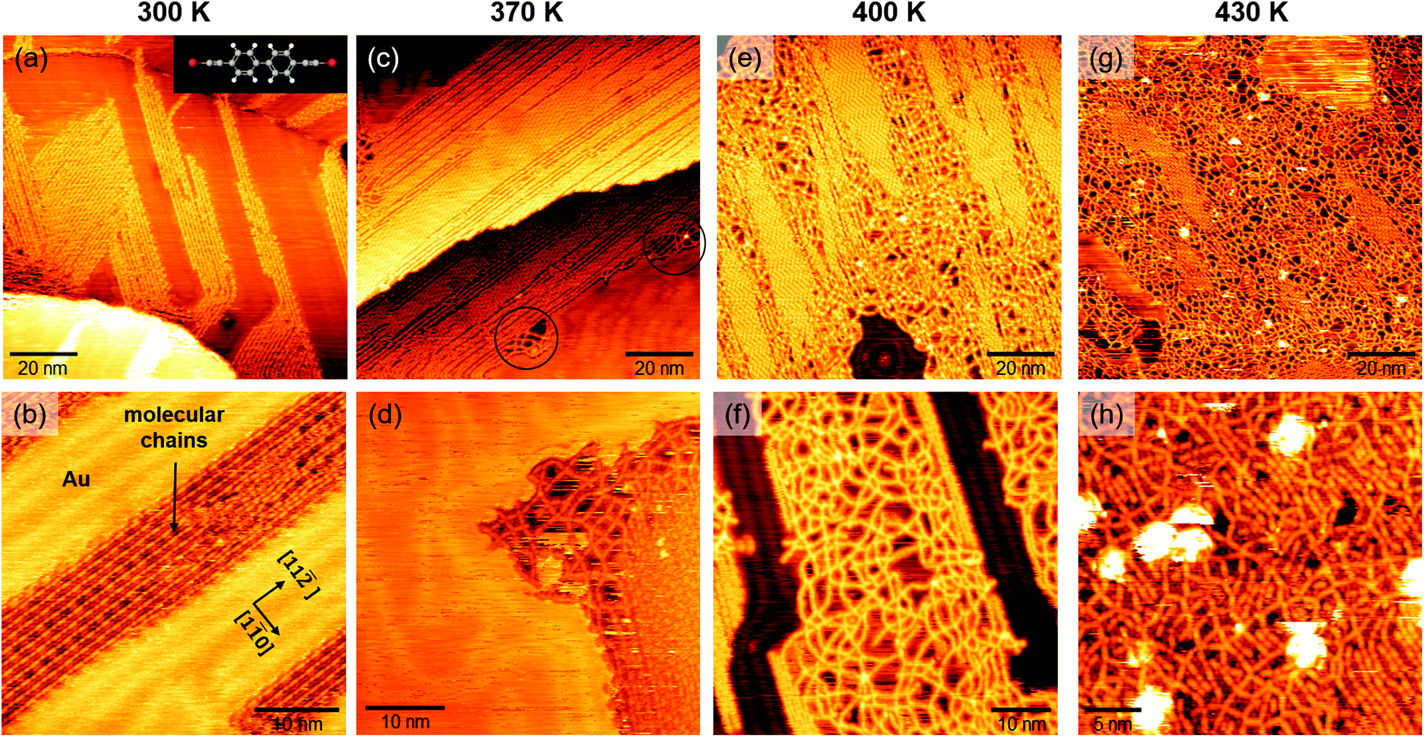 | ||
Fig. 1 STM images of on-surface synthesized sp–sp2 C polymers. 100 × 100 nm2 images are reported in the upper row, and smaller-scale ones in the lower row. (a) STM image of the sample observed after deposition of bBEBP molecules on Au(111) at room temperature. Inset: Ball-and-stick structure of a bBEBP molecule, where red dots represent Br atoms, grey dots C atoms and white dots H atoms. (b) Close-up of a surface region showing linear wires aligned along the [11![[2 with combining macron]](https://www.rsc.org/images/entities/char_0032_0304.gif) ] Au(111) direction. (c) and (d) STM images taken after annealing at 370 K. Black circles in (c) indicate locally disordered regions, as that shown in (d) at higher resolution. (e) and (f) STM images taken after annealing at 400 K. (g) and (h) STM images taken after annealing at 430 K. ] Au(111) direction. (c) and (d) STM images taken after annealing at 370 K. Black circles in (c) indicate locally disordered regions, as that shown in (d) at higher resolution. (e) and (f) STM images taken after annealing at 400 K. (g) and (h) STM images taken after annealing at 430 K. | ||
3.1 Structural and electronic properties
To study thermal effects on the morphology and structure of carbon atomic wires, we performed in situ STM measurements right after deposition of the molecular precursor on Au(111) and then, successively, after annealing the samples at different temperatures in UHV. We acquired all the STM images at RT, for direct comparison of the morphology and structure with vibrational Raman spectra. Fig. 1 reports several STM images. Images acquired on the as-deposited sample (i.e. at 300 K, Fig. 1a and b); images acquired on samples annealed at 370 K (Fig. 1c and d), 400 K (Fig. 1e and f), and 430 K (Fig. 1g and h). 100 × 100 nm2 and smaller-scale images are reported, respectively, in the upper and lower row of Fig. 1. After deposition, we observe the formation of linear wires, several tens of nm long, which assemble in compact domains having well-defined orientation (Fig. 1a). As shown in Fig. 1b, the molecular wires are oriented along the [11] crystallographic directions of the Au(111) surface. Ordered domains of linear wires are observed also after annealing at 370 K, Fig. 1c. However, a locally-disordered arrangement is observed at some small regions (e.g. those circled in black in Fig. 1c), especially occurring at domain borders (Fig. 1d). The tendency to acquire a disordered arrangement becomes evident after annealing at higher temperatures: at 400 K and 430 K (Fig. 1e and g, respectively) we observe few ordered regions, surrounded by an amorphous network of randomly oriented wires which apparently cross-link with each other (Fig. 1f–h). The formation of this disordered network is probably triggered by the thermal activation of highly reactive wire terminations, which may possibly cross-link with neighboring wires starting the propagation of a disordered phase.
High-resolution STM images allow us to observe the sp–sp2 wires structure at the molecular scale. Fig. 2a and b shows well-ordered polymers formed right after deposition. The on-surface synthesis is known to be catalyzed by surface gold atoms which substitute the terminal bromines of bBEBP molecules, leading to the formation of organometallic (i.e. metalated) wires.28 This interpretation is supported by the simulated STM image shown in Fig. 2(e), obtained from the theoretical model depicted in Fig. 2(c)–(d) and described hereafter. Taking into account the experimentally-determined direction for the organometallic wire (Fig. 1(b)), the simulations are performed for a model with the wires aligned along the [11] surface direction, as seen in experiment. Note that this geometry differs from previous calculations,28,45 where the polymer was aligned along, or at a small angle from the [1![[1 with combining macron]](https://www.rsc.org/images/entities/char_0031_0304.gif) 0] close-packed direction. The unambiguous identification of the wire orientation has been possible through the large scale images in which the herringbone Au(111) reconstruction can be easily identified.
0] close-packed direction. The unambiguous identification of the wire orientation has been possible through the large scale images in which the herringbone Au(111) reconstruction can be easily identified.
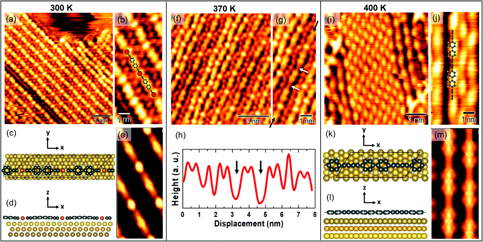 | ||
| Fig. 2 (a) STM image resolving the structure of linear sp1–sp2 wires (0.4 V, 0.6 nA). (b) Magnification of image (a). (c) and (d) Top and side view of the ball-and-stick model for the organometallic chain, as adopted in the simulations. (e) DFT-simulated STM image (empty states, 2 Å tip–surface distance) of the organometallic chain. (f) STM image taken after annealing at 370 K (0.4 V, 0.6 nA). (g) Magnification of image (f). (h) Line-profile on the wire indicated in image (g). (i) STM image taken after post-annealing at 400 K (0.4 V, 0.6 nA). (j) Magnification of image (i). (k) and (l) Top and side view of the ball-and-stick model of the demetalated molecules, as adopted in the simulations. (m) Simulation of STM images by DFT calculations (empty states, 2 Å tip–surface distance) for the demetalated molecule. | ||
Since the unit length of the polymer is intermediate between 3 and 4 Au–Au distances along the [11] direction, we have chosen to consider in the calculations an average length of 3.5 Au–Au distances with a unit cell containing two monomers threading 7 Au surface unit cells. This constraints applies an overall 6.7% strain to the polymer compared to its unit length relaxed in vacuum, similar to the previous studies.45 The distance between adjacent chains in the orthogonal in-plane direction ([10]) is taken equal to 8.65 Å. The adopted periodicity is slightly smaller than that determined from the experiments but, due to the negligible inter-molecule interaction, it gives reliable results by avoiding the computational effort to include further substrate atoms in the simulation. The bond lengths of the adsorbed polymer are 150 pm, 127 pm, and 221 pm for the triple and single C–C bond, and the C–Au bond, respectively, to be compared with the 140 pm, 125 pm, and 195 pm of the free-standing polymer at its equilibrium geometry. The increase of the bond lengths is not only due to strain but also to the overall outward bending of the polymer that displays a minimum distance from the substrate (253 pm) in correspondence of the Au metal atom, due to the stronger Au–Au interaction, while the phenyl groups sit 34 pm farther out. The phenyl groups appear flattened down to the surface, compared to the gas phase, where they are free to rotate around the polymer axis, and end up forming 60° mutual angles in the equilibrium geometry. The same structure and corrugation is found in both the molecular units contained in the periodically repeated unit cell.
The STM simulations allow us to identify the double protrusion observed in the experiments as due to biphenyl groups. The bright spot of circular shape located midway between two successive biphenyl groups can be associated to the Au atom in the organometallic chain. The structural relaxation (Fig. 2(d)) reveals that the phenyl-related signal is morphologically enhanced by the bending of the organometallic chain. The sp-carbon atomic chain contribution is hardly resolved in the STM signal, due to the experimental resolution, while it can be identified in the simulations as a weakly bright region between the Au-related feature and the biphenyl one. The less bright spots observed in the experiments between two adjacent chains, Fig. 2(b), can be identified as due to Br atoms detached from the molecular structure during the reaction at the surface, in agreement with what is observed in dimer formation.28 The absence of such spots in the simulations is fully consistent with the model, not including bromine atoms.
As the temperature increases, gold adatoms in the chain get released and the CC homocoupling takes place, resulting in the formation of a polymeric sp–sp2 carbon wire.28 This mechanism can be observed after annealing at 370 K, as shown in Fig. 2f and g. The two white arrows in Fig. 2g mark two sites where the Au bright spots are missing, indicating the local absence of Au atoms in the chain, as also highlighted by the line profile in Fig. 2h. Increasing the temperature to 400 K pushes the CC homocoupling process forward, so that a larger fraction of demetalated chains can be observed (Fig. 2i). The high-resolution STM image of Fig. 2j displays 7 Å-wide spots, corresponding to the biphenyl group, connected by a weaker straight signal related to the sp-carbon-based chains, and no fingerprint of Au atoms within the chain. The simulated STM image reported in Fig. 2m agrees with this assignment.
Given the absence of a preferential orientation in the experiments, to describe the demetalated wire we choose a model oriented along the [10] direction, which allows us to consider a smaller periodic cell containing a single unit. The polymer and the surface are indeed matched with a periodicity of 5 Au(111) surface unit cells along [10], leading to a 4.5% of strain of the molecule. The simulation cells displays repeated wires at a distance of 7.49 Å along the orthogonal direction.
Notably, we have verified that the theoretical STM image is not sensitive to the orientation of the molecule on the surface: the simulation of the metalated polymer oriented along the close packed direction, as in ref. 45, is indeed qualitatively very similar to that reported in Fig. 2(e).
Fig. 2(k) and (l) report the equilibrium geometry of the demetalated polymer. In this case the molecule is flat, at a larger distance from the surface (∼280 pm) compared to the RT case, as expected due to the weaker interaction with the surface upon removal of the Au atom from the chain.
We should notice, however, that even after annealing at higher temperatures, e.g. 430 K, we still observe occasional small areas occupied by metalated chains, i.e. with gold atoms still appearing in between successive diphenyl groups.
Surface local electronic properties have been characterized by STS at RT. We performed open-loop point-spectroscopy measurements on the organometallic wires (i.e. metalated chains) observed after deposition (region B in the inset of Fig. 3) and on the Au substrate regions not occupied by molecular wires (region A). Fig. 3 shows the average dI/dV spectra of the two investigated regions. The red curve, taken over the A region, shows a pronounced peak around −0.5 eV relative to the Fermi energy (0 eV), compatible with the Au(111) Shockley state. The black curve, taken over a region rich in carbon atomic wires, shows a peak around −0.75 eV, which may origin from a shift of the Shockley state energy due to the interaction with wire electronic states. The rapid increase of the black spectrum for energies lower than −1 eV represents a signature of the polymer-associated surface electronic properties. Such characteristic behavior can be interpreted as the onset of the band of occupied electronic states. Conversely, no substantial differences can be seen in the conduction band. We were not able to record reproducible STS data on the homocoupled carbon wires probably due to the disordered morphology.
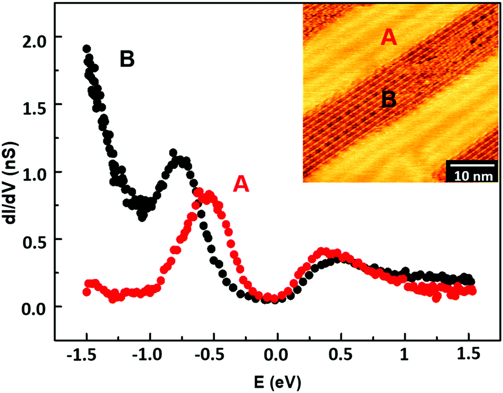 | ||
| Fig. 3 Average dI/dV curves taken on the as-deposited sample over the A (bare gold, red dots) and B (carbon wires, black dots) regions shown in the inset. | ||
For a precise interpretation of the experimental electronic spectra, we report the computed PDOS on the metalated wires and on the Au surface layer, Fig. 4.
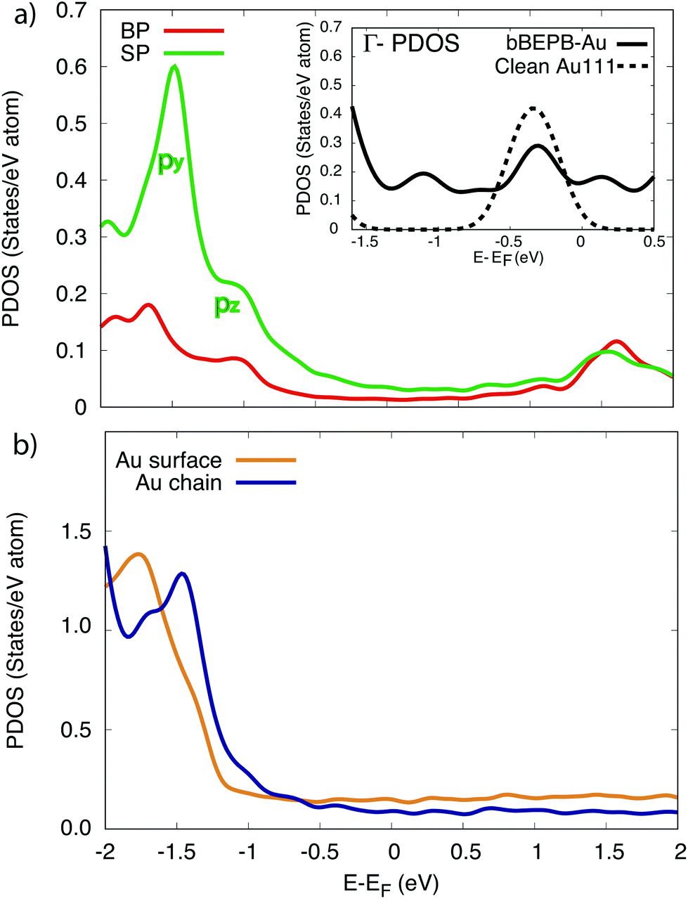 | ||
Fig. 4 Projected density of states (PDOS) on (a) the C atoms in the metalated molecule; (b) the surface-layer Au atoms and within the wire, according to the model in Fig. 2c and d. Red curve: Averaged PDOS of the biphenyl groups (BP). Green line: Averaged PDOS of the sp1-carbon chain (SP). Orange line: Averaged PDOS of the Au surface atoms. Blue line: Averaged PDOS of the Au atoms in the chain. Inset of panel (a): PDOS at the  point. Solid line: PDOS of the Au surface layer upon the deposition of the organometallic chain. Dashed line: PDOS of the surface layer of the clean Au(111) surface. point. Solid line: PDOS of the Au surface layer upon the deposition of the organometallic chain. Dashed line: PDOS of the surface layer of the clean Au(111) surface. | ||
The PDOS on the C atoms (Fig. 4a) shows a relevant contribution from molecular states below the Fermi level, at energies lower than −1 eV. These states are mainly localized on the sp chain, with py and pz character. The px states are found lower in energy. The lowest empty molecular states exhibit a peak at 1.5 eV. Further high-intensity features arise at higher energies, outside the range reported here. The PDOS on Au atoms in the chain shows a partial hybridization with the in-plane molecular orbitals and with the underlying substrate (peak at −1.3 eV in the blue curve).
The mild feature at −1.3 eV in the PDOS on the outermost substrate layer (orange curve) can be indeed related to the surface-molecule interaction, while the rise observed below −1.5 eV corresponds to the onset of the d-band of Au(111).
Additional insight is gained by examining the density of states at the  point of the surface Brillouin zone, being those characterized by the slowest decay in vacuum, i.e. the larger overlap with the tip states resulting in a larger detection probability. Moreover, the PDOS at the
  point allows us to evidence the contribution of the Shockley state.
The inset of Fig. 4 compares the PDOS at the  of the surface Au atoms in the presence of the metalated polymer (solid line) and the PDOS on the outermost layer of the clean Au(111) surface (dashed line).
Calculations show a partial quenching of the Shockley state at the interface with the molecule and an increase of spectral weight of the states ∼−1 eV below the Fermi level, that can be related to the interaction with pz states of the molecule. These results are consistent with the shift and the reduced intensity of the peak observed in STS spectra. Moreover, the contribution of the electronic states on the molecule, starting at −1.5 eV, is in agreement with the rise observed in the STS spectrum at the same energy.
3.2 Raman spectroscopy and vibrational properties
We investigated the vibrational properties by ex situ Raman spectroscopy and by DFT calculation of the Raman response, see Fig. 5. We were able to record spectra at room temperature from less than one monolayer of sp–sp2 carbon wires deposited on Au(111) and to follow their evolution as a function of the annealing temperature from 370 K to 430 K, see Fig. 1. Important differences are observed when comparing the spectra of the sample annealed at different temperatures to that of the precursor prior to sublimation, measured in powder form. The spectrum of the precursor molecule is characterized by features in three main spectral regions. The main 2190 cm−1 peak in the high-wavenumber region (2000–2200 cm−1) is the fingerprint of the acetylenic sp-carbon; the intermediate region has a peak at 1602 cm−1 due to sp2 carbon in the phenyl rings and a few weak features are present in the low-wavenumber region (1100–1300 cm−1). DFT calculations agree well with the experimental spectrum of the precursor and allow us to assign these peaks in details. The peak at 2220 cm−1 (computed at an unscaled 2314 cm−1) is due to CC stretching vibrations localized on the triple bonds of the acetylenic chains. The peak at 1602 cm−1 (computed at an unscaled 1669 cm−1) is attributed to CC stretching modes localized on the biphenyl groups. The triplet of peaks observed at 1190, 1250 and 1285 cm−1 are predicted at 1160, 1230 and 1272 cm−1 (1208 cm−1, 1282 cm−1 and 1325 cm−1 unscaled values). The first peak is due to CH wagging vibrations; the second is associated to CC stretching modes localized on the single CC bond between phenyls and triple CC bonds coupled to CH wagging vibrations; the 1272 cm−1 peak involves a significant contribution of the CC stretching of the bond connecting the two phenyls coupled again to CH waggings (sketches of these normal modes are reported in the ESI†). | ||
| Fig. 5 Vibrational spectra obtained by Raman measurements and DFT calculations. (left) Experimental Raman spectra of the molecular precursor and linear chains on Au(111) surface after annealing the sample at different temperatures. (right) DFT calculations of the molecular precursor (black) and of the homocoupled polymer on Au(111) (red). The DFT spectra have been rescaled to match the CC stretching mode of the phenyl ring at 1602 cm−1. | ||
After evaporation of the precursor on Au(111) and annealing in UHV, ex situ spectra show a new feature in the sp-carbon region at ∼2150 cm−1 which increases in intensity relative to the peak at 2190 cm−1 (their intensity ratio I(2150)/I(2190) increases from 0.5 to more than 2) and becomes narrower with increasing the annealing temperature (see Fig. 6(a)–(c)). In addition, a weak peak emerges at about 2020 cm−1 whose width decreases with the annealing temperature. In the other spectral regions the peak at approximately 1600 cm−1 shifts to lower frequencies (from 1602 to 1583 cm−1) while small changes only characterize the low-frequency region. The observed modifications can be interpreted in light of DFT calculations and on the basis of the results obtained by STM.
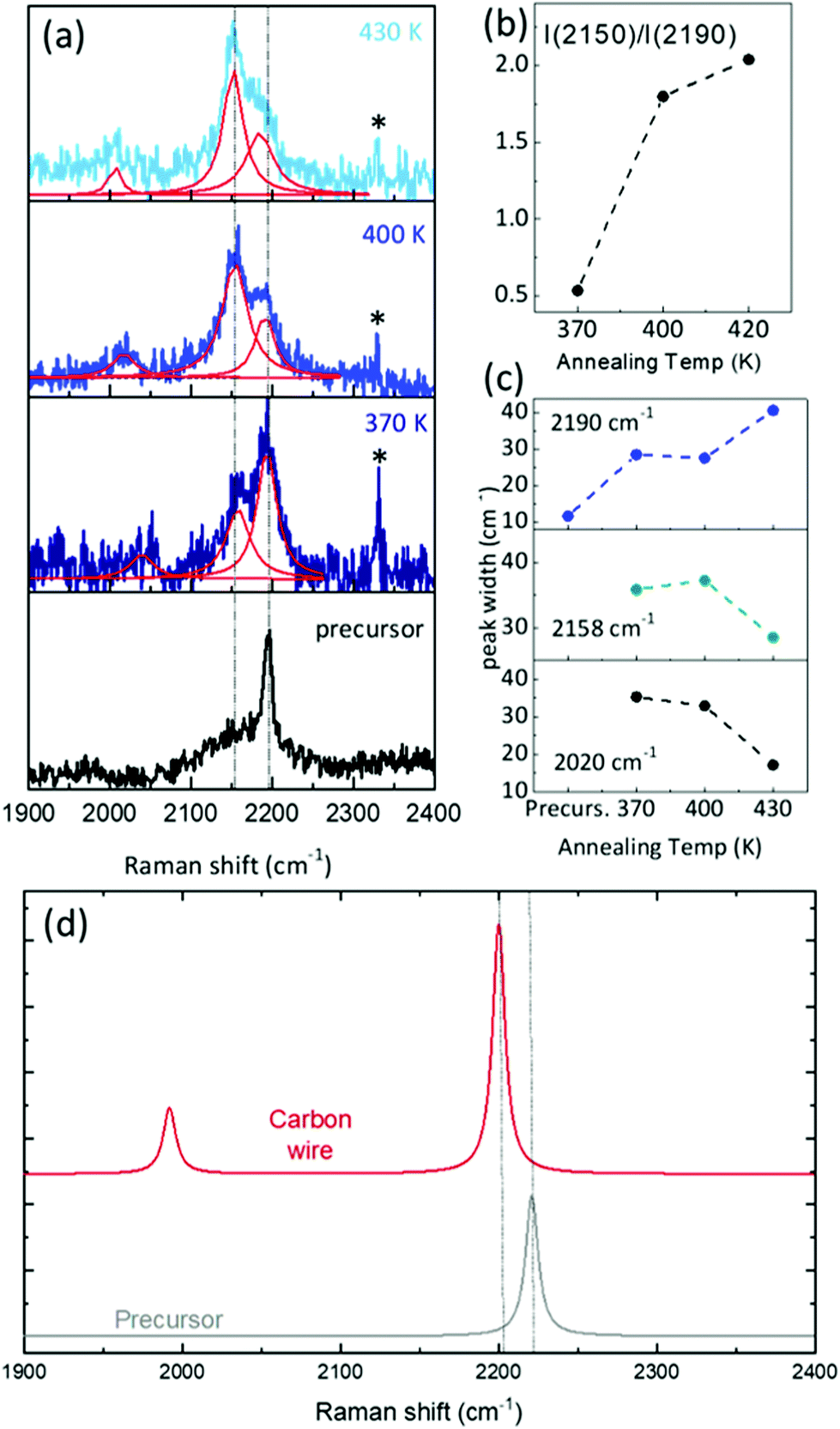 | ||
| Fig. 6 (a) Close-up of the experimental Raman in the region 1800–2400 cm−1 relevant to sp carbon. The peak of atmospheric molecular nitrogen is labeled with *. (b) Annealing-temperature dependence of the intensity ratio of the peaks at 2150 and 2190 cm−1. (c) Full width at half maximum (FWHM) of the main peaks as a function of the annealing temperature. (d) Close-up of simulated Raman spectra for the precursor molecule and the polymeric sp–sp2 wires. | ||
To compute the vibrations of the carbon chain deposited on the surface, the full DFT model as sketched in Fig. 2(c) and (d) is not a viable possibility. The reason resides in the large computational cost of the hybrid functionals and large Gaussian basis sets needed to describe the vibrational response of the carbon chains accurately, which becomes too expensive to fully describe the Au(111) surface in periodic boundary conditions. Hence, we adopt a simplified model as a compromise between accuracy and computational cost: a system consisting of a homocoupled precursor dimer interacting with a gold cluster of 8 atoms. Calculations of the Raman response predict two marker bands of the sp-carbon chains in the high-frequency region. One peak is found at 2200 cm−1 (2292 cm−1 unscaled value) and corresponds to a normal mode of vibrations still localized on the sp-carbon segments but described now as the CC stretching of the triple bond coupled to the surrounding single CC bonds. In particular, the bonds involved here are those less influenced by the gold cluster. This band is thus very similar to the one typically found in the Raman spectrum of polyynes (i.e. due to the setting on of the so-called effective conjugation coordinate ECC collective mode32,46). Here this mode is perturbed by the non-bonded interaction with the Au cluster. As a result, this peak falls at a lower wavenumber than the band of the precursors, in good agreement with the experimental spectra where a new feature is also observed at slightly lower wavenumber than the precursor and gradually increases in intensity with the annealing temperature, following the formation of the polymeric chains observed in the STM images. The comparison with DFT calculations allows us to confirm the attribution to carbon wires formed on the Au surface. In addition to this band, a second one is predicted at 1992 cm−1 (2075 cm−1 unscaled value), possibly corresponding to the weak feature observed at 2020 cm−1 for increasing temperature. The normal mode associated to this peak can be described as a CC stretching vibration mainly localized on the triple CC bond closer to the gold cluster. Analyzing the CC bond distances and their valence force constants (fCC) a picture of the effects involved can be found. The triple CC bonds in the carbon wire model have lengths of 121 pm and 125 pm, with fCC values of 1584 and 414 N m−1 respectively. By comparing these bonds with those of the precursor (i.e. 121 pm, for the triple CC bonds and fCC = 1662 N m−1), we observe how the non-covalent interaction with the gold cluster modulates significantly the strength and hence the geometry of the bonds in the sp-carbon sections, modulating also their Raman response and generating peculiar marker bands in the spectra.
These results allow us to identify the Raman spectrum of sp–sp2 polymeric carbon atomic wires on Au(111). The peak at 2150 cm−1 with its increasing intensity with the annealing temperature is a clear signature of the formation of homocoupled bonding to produce sp–sp2 polymeric carbon atomic wires. The weak peak at 2020 cm−1 is in agreement with theoretical predictions. STM analysis shows that the homocoupling reaction happens in a wide temperature window leaving mixed regions in which homocoupled chains coexist with metalated chains. The presence of the peak at 2190 cm−1 seems to indicate the possible presence of unreacted precursors on the surface even though it cannot be clearly confirmed by our STM analysis. We were not able to record a spectrum from the as deposited sample fully corresponding to the metalated carbon wire where the coupling is mediated by gold adatoms. The reason is a very low signal-to-noise ratio which hindered the possibility to acquire reliable spectra. Indeed, we experimentally observe an increase in the signal-to-noise ratio for increasing the annealing temperature. Accordingly, the time needed to acquire the spectra is different and this is evident by looking at the peak of the atmospheric molecular nitrogen (labeled with * in Fig. 6(a)), whose intensity is proportional to the collection time and decreases significantly with the increase of the annealing temperature. The broad band at about 1580 cm−1 appearing at high annealing temperatures as a weak shoulder of the peak at 1602 cm−1 (see Fig. 5) can be attributed to sp2 carbon amorphous phase resulting from the crosslinking of carbon atomic wires in the disordered regions observe in STM (see Fig. 1).
As for simulations, as also evidenced by Kroto et al. for similar sp-carbon systems47 the results of DFT calculations are affected by the choice of a finite-size molecular model. Ours is certainly not large enough to describe the real gold surface. Different models have been chosen to describe the interaction with the gold substrates and the related Raman spectra are affected significantly by this choice (see the ESI†). Also for the sp–sp2 polymeric wire, we adopted the dimer as a reduced version of the longer wires, after checking computationally that Raman signal is not affected by increasing the length of the model (i.e. number of oligomers) since the phenyl groups interrupt the conjugation (see ESI†). The small frequency mismatch of sp-carbon Raman peaks between DFT calculations and experiments can be also due to the distortion of the sp–sp2 when interacting with the gold cluster. This distortion is the effect of the adopted model and it is not present in calculations of the structure and STM images which adopt a periodic Au(111) surface. Based on these considerations and on the similar trends observed in all the models we investigated, DFT calculations may describe the qualitative trends observed in the experimental spectra, allowing for an interpretation of the experiments.
As a final issue, since our sp–sp2 polymeric wires represent an example of long linear 1D carbon with quite good stability, it is interesting to compare them with other relevant sp-carbon structures. In this context, one example is the ideal case of the infinite carbyne, which is nicely approached by extremely long chains inside a carbon nanotube.5 This system is different concerning both the synthesis methods and the Raman spectrum observed. In particular, the Raman spectrum of long linear chain in the nanotube shows an sp-carbon peak at about 1800 cm−1. The wavenumber value is much lower than the case of short polyynes (showing a frequency at about 2200 cm−1) and it is consistent with the well-known redshift expected for increasing wire length. Conversely, in our system, phenyl groups interrupt the conjugation path, which cannot extend following the overall length of the wire (i.e. the number of oligomeric units). In this sense, from the vibrational point of view, our polymeric wires with a Raman peak at about 2200 cm−1 are more similar to a phenyl-terminated polyyne with 4 sp-carbon atoms rather than a long linear carbon chain.48 As observed above, a Raman peak at about 2000 cm−1 is also observed, due to the interaction of the wire with the gold surface.
On the other hand, our system appears to be more closely related to a graphdiyne nanoribbon and in particular it would correspond ideally to the narrowest armchair nanoribbon of γ-graphdiyne. Since no data are present in the literature on Raman spectra of these nanoribbons, a comparison can be done with the calculated Raman spectrum of an extended 2D graphdiyne crystal, as reported in ref. 49. As expected, some similarities are observed, such as the frequency of the sp-carbon peak at about 2200 cm−1 and the Raman modes related to vibrations of the phenyl ring at about 1500–1600 cm−1. In extended graphdiyne, however, some of these peaks appear to be split, due the 2D extension of this system and the presence of some other Raman active modes which cannot be found in our one-dimensional system. Again, the additional peak at about 2000 cm−1 is a peculiarity of the present system, resulting from the presence of the gold surface.
4 Conclusions
We report the atomic-scale structure, electronic and vibrational properties of long linear sp–sp2 polymeric carbon nanostructures on Au(111) investigated by STM/STS and Raman spectroscopy. We characterize the surface electronic density of states as resulting from the hybridization between the molecular levels residing on the polymer and the metallic bands of the substrate. The occupied states, residing on the sp chain sections of the polymer determine a characteristic peaks below the Fermi energy. Concerning the structural properties, Raman spectroscopy provide complementary information to the high-resolution STM imaging, allowing us to follow the formation of sp–sp2 polymeric carbon atomic wires after the deposition of sp-carbon-based oligomer on Au(111). Raman spectra show a new peak shifted at lower frequency with respect to the pristine acetylenic band of the precursor molecule indicating the increased length of the wire as a consequence of the homocoupling reaction. Such new feature in the sp-carbon spectral region increases in intensity by increasing the temperature in agreement with the formation of sp–sp2 carbon atomic wires by homocoupling, as observed by STM. An additional Raman peak at significantly lower frequency appears due to the bond softening promoted by the interaction with gold. Although overall the polymeric wires investigated here are quite long compared to the sp-carbon atomic wires usually available from organic synthesis, they cannot be considered as a model approaching the infinite wire carbyne, since the sp conjugation is here limited to the relatively short C4 sections. The phenyl groups which seem to support the stability are also responsible for the interruption of the π-electron conjugation. As a result neither in experiment nor in DFT simulations do we observe any length-dependent effects. In this respect, the decoupling between the overall length of the polymer and the extension of the conjugation could be exploited for novel structures. Indeed, the control of the oligomeric unit through the choice of the precursor would pave the way to the tuning of the properties of long polymeric carbon atomic wires on metal surfaces. In the light of the obtained experimental results, UHV-STM/STS and ex situ Raman spectroscopy techniques represent a powerful and non destructive strategy to investigate novel sp-carbon based nanostructures with a great potential for the characterization of other novel 1D and 2D structures, such as graphyne and graphdiyne.Conflicts of interest
There are no conflicts to declare.Acknowledgements
We thank Mario Italo Trioni for useful discussions and Riccardo Improta for preliminary work done during his Master Thesis. AR, FT, AM, VR, ALB and CSC acknowledge funding from the European Research Council (ERC) under the European Union's Horizon 2020 research and innovation programme ERC - Consolidator Grant (ERC CoG 2016 EspLORE grant agreement No. 724610, website: http://www.esplore.polimi.it). SA, GF, NM, and GO acknowledge the CINECA supercomputing grant project HP10C3S9Z0 under Iscra C initiative for the availability of high performance computing resources and support. G. O. and S. A. acknowledge funding from the EU-H2020 Research and Innovation program under Grant Agreement No. 654360 – NFFA-Europe.References
- A. Hirsch, Nat. Mater., 2010, 9, 868–871 CrossRef CAS PubMed.
- C. S. Casari, M. Tommasini, R. R. Tykwinski and A. Milani, Nanoscale, 2016, 8, 4414–4435 RSC.
- M. Liu, V. I. Artyukhov, H. Lee, F. Xu and B. I. Yakobson, ACS Nano, 2013, 7, 10075–10082 CrossRef CAS PubMed.
- L. Shi, P. Rohringer, M. Wanko, A. Rubio, S. Wasserroth, S. Reich, S. Cambre, W. Wenseleers, P. Ayala and T. Pichler, Phys. Rev. Mater., 2017, 1, 075601 CrossRef.
- L. Shi, P. Rohringer, K. Suenaga, Y. Niimi, J. Kotakoski, J. C. Meyer, H. Peterlik, M. Wanko, S. Cahangirov, A. Rubio, Z. J. Lapin, L. Novotny, P. Ayala and T. Pichler, Nat. Mater., 2016, 15, 634–639 CrossRef CAS.
- W. A. Chalifoux and R. R. Tykwinski, Nat. Chem., 2010, 2, 967–971 CrossRef CAS PubMed.
- F. Hu, C. Zeng, R. Long, Y. Miao, L. Wei, Q. Xu and W. Min, Nat. Methods, 2018, 15, 194–200 CrossRef CAS PubMed.
- F. Cataldo, O. Ursini, A. Milani and C. S. Casari, Carbon, 2018, 126, 232–240 CrossRef CAS.
- Y. Zhu, H. Bai and Y. Huang, Synth. Met., 2015, 204, 57–64 CrossRef CAS.
- Y. Zhu, H. Bai and Y. Huang, ChemistryOpen, 2016, 5, 78–87 CrossRef CAS PubMed.
- P. Bonardi, S. Achilli, G. F. Tantardini and R. Martinazzo, Phys. Chem. Chem. Phys., 2015, 18413–15425 RSC.
- Z. Zanolli, G. Onida and J. C. Charlier, ACS Nano, 2010, 4, 5174–5180 CrossRef CAS PubMed.
- A. L. Ivanovskii, Prog. Solid State Chem., 2013, 41, 1–19 CrossRef CAS.
- P. Ruffieux, S. Wang, B. Yang, C. Sanchez-Sanchez, J. Liu, T. Dienel, L. Talirz, P. Shinde, C. Pignedoli, D. Passerone, T. Dumslaff, X. Feng, K. Möllen and R. Fasel, Nature, 2016, 531, 489–492 CrossRef CAS PubMed.
- H. Zhang, H. Lin, K. Sun, L. Chen, Y. Zagranyarski, N. Aghdassi, S. Duhm, Q. Li, D. Zhong, Y. Li, K. Müllen, H. Fuchs and L. Chi, J. Am. Chem. Soc., 2015, 137, 4022–4025 CrossRef CAS PubMed.
- A. Basagni, F. Sedona, C. A. Pignedoli, M. Cattelan, L. Nicolas, M. Casarin and M. Sambi, J. Am. Chem. Soc., 2015, 137, 1802–1808 CrossRef CAS PubMed.
- T. A. Pham, B. V. Tran, M.-T. Nguyen and M. Stöhr, Small, 2017, 13, 1603675 CrossRef PubMed.
- Q. Shen, H.-Y. Gao and H. Fuchs, Nano Today, 2017, 13, 77–96 CrossRef CAS.
- J. Liu, Q.-W. Chen and K. Wu, Chin. Chem. Lett., 2017, 28, 1631–1639 CrossRef CAS.
- F. Klappenberger, Y.-Q. Zhang, J. Björk, S. Klyatskaya, M. Ruben and J. V. Barth, Acc. Chem. Res., 2015, 48, 2140–2150 CrossRef CAS PubMed.
- P. A. Held, H. Fuchs and A. Studer, Chem. – Eur. J., 2017, 23, 5874–5892 CrossRef CAS PubMed.
- Q. Fan, J. Gottfried and J. Zhu, Acc. Chem. Res., 2015, 48, 2484–2494 CrossRef CAS PubMed.
- B. Cirera, Y.-Q. Zhang, J. Björk, S. Klyatskaya, Z. Chen, M. Ruben, J. V. Barth and F. Klappenberger, Nano Lett., 2014, 14, 1891–1897 CrossRef CAS PubMed.
- H. Zhou, J. Liu, S. Du, L. Zhang, G. Li, Y. Zhang, B. Z. Tang and H.-J. Gao, J. Am. Chem. Soc., 2014, 136, 5567–5570 CrossRef CAS PubMed.
- Q. Sun, R. Zhang, J. Qiu, R. Liu and W. Xu, Adv. Mater., 2018, 30, 1705630 CrossRef PubMed.
- V. Derycke, P. Soukiassian, A. Mayne, G. Dujardin and J. Gautier, Phys. Rev. Lett., 1998, 81, 5868–5871 CrossRef CAS.
- Q. Sun, L. Cai, S. Wang, R. Widmer, H. Ju, J. Zhu, L. Li, Y. He, P. Ruffieux, R. Fasel and W. Xu, J. Am. Chem. Soc., 2016, 138, 1106–1109 CrossRef CAS PubMed.
- Q. Sun, L. Cai, H. Ma, C. Yuan and W. Xu, ACS Nano, 2016, 10, 7023–7030 CrossRef CAS PubMed.
- Q. Sun, B. V. Tran, L. Cai, H. Ma, X. Yu, C. Yuan, M. Stöhr and W. Xu, Angew. Chem., 2017, 129, 12333–12337 CrossRef.
- Q. Sun, X. Yu, M. Bao, M. Liu, J. Pan, Z. Zha, L. Cai, H. Ma, C. Yuan, X. Qiu and W. Xu, Angew. Chem., Int. Ed., 2018, 57, 4035–4038 CrossRef CAS PubMed.
- C.-H. Shu, M.-X. Liu, Z.-Q. Zha, J.-L. Pan, S.-Z. Zhang, Y.-L. Xie, J.-L. Chen, D.-W. Yuan, X.-H. Qiu and P.-N. Liu, Nat. Commun., 2018, 9, 2322 CrossRef PubMed.
- A. Milani, M. Tommasini, V. Russo, A. L. Bassi, A. Lucotti, F. Cataldo and C. S. Casari, Beilstein J. Nanotechnol., 2015, 6, 480–491 CrossRef PubMed.
- L. Ravagnan, F. Siviero, C. Lenardi, P. Piseri, E. Barborini, P. Milani, C. Casari, A. Li Bassi and C. Bottani, Phys. Rev. Lett., 2002, 89, 285506 CrossRef CAS PubMed.
- G. Grasso, L. D'Urso, E. Messina, F. Cataldo, O. Puglisi, G. Spoto and G. Compagnini, Carbon, 2009, 47, 2611–2619 CrossRef CAS.
- F. Cataldo, Carbon, 2005, 43, 2792–2800 CrossRef CAS.
- T. Wakabayashi, H. Tabata, T. Doi, H. Nagayama, K. Okuda, R. Umeda, I. Hisaki, M. Sonoda, Y. Tobo, T. Minematsu, K. Hashimoto and S. Hayashi, Chem. Phys. Lett., 2007, 433, 296–300 CrossRef CAS.
- A. Lucotti, M. Tommasini, M. Del Zoppo, G. Castiglioni, C. Zerbi, F. Cataldo, C. S. Casari, A. Li Bassi, V. Russo, M. Bogana and C. E. Bottani, Chem. Phys. Lett., 2006, 417, 78–82 CrossRef CAS.
- J. M. Soler, E. Artacho, J. D. Gale, A. García, J. Junquera, P. Ordejón and D. Sánchez-Portal, J. Phys.: Condens. Matter, 2002, 14, 2745 CrossRef CAS.
- J. P. Perdew, K. Burke and M. Ernzerhof, Phys. Rev. Lett., 1996, 77, 3865–3868 CrossRef CAS PubMed.
- S. Grimme, J. Comput. Chem., 2006, 27, 1787–1799 CrossRef CAS PubMed.
- J. Tersoff and D. R. Hamman, Phys. Rev. B: Condens. Matter Mater. Phys., 1985, 31, 805 CrossRef CAS PubMed.
- M. J. Frisch, G. W. Trucks, H. B. Schlegel, G. E. Scuseria, M. A. Robb, J. R. Cheeseman, G. Scalmani, V. Barone, G. Petersson, H. Nakatsuji, X. Li, M. Caricato, A. Marenich, J. Bloino, B. G. Janesko, R. Gomperts, B. Mennucci, H. P. Hratchian, J. V. Ortiz, A. F. Izmaylov, J. L. Sonnenberg, D. Williams-Young, F. Ding, F. Lipparini, F. Egidi, J. Goings, B. Peng, A. Petrone, T. Henderson, D. Ranasinghe, V. G. Zakrzewski, J. Gao, N. Rega, G. Zheng, W. Liang, M. Hada, M. Ehara, K. Toyota, R. Fukuda, J. Hasegawa, M. Ishida, T. Nakajima, Y. Honda, O. Kitao, H. Nakai, T. Vreven, K. Throssell, J. A. Montgomery, J. Peralta Jr., F. Ogliaro, M. Bearpark, J. J. Heyd, E. Brothers, K. N. Kudin, V. N. Staroverov, T. Keith, R. Kobayashi, J. Normand, K. Raghavachari, A. Rendell, J. C. Burant, S. S. Iyengar, J. Tomasi, M. Cossi, J. M. Millam, M. Klene, C. Adamo, R. Cammi, J. W. Ochterski, R. L. Martin, K. Morokuma, O. Farkas, J. B. Foresman and D. J. Fox, Gaussian 09, Revision A.02, Gaussian, Inc., Wallingford CT, 2016 Search PubMed.
- A. Milani, M. Tommasini and G. Zerbi, J. Chem. Phys., 2008, 128, 064501 CrossRef PubMed.
- D. Figgen, G. Rauhut, M. Dolg and H. Stoll, Chem. Phys., 2005, 311, 227 CrossRef CAS.
- G. Fratesi, S. Achilli, N. Manini, G. Onida, A. Baby, A. Ravikumar, A. Ugolotti, G. P. Brivio, A. Milani and C. S. Casari, Materials, 2018, 11, 2556 CrossRef PubMed.
- M. T. C. Castiglioni and G. Zerbi, Philos. Trans. R. Soc. London, Ser. A, 2004, 362, 2425 CrossRef PubMed.
- P. Tarakeshwar, P. R. Buseck and H. W. Kroto, J. Phys. Chem. Lett., 2016, 7, 1675–1681 CrossRef CAS PubMed.
- A. Milani, A. Lucotti, V. Russo, M. Tommasini, F. Cataldo, A. Li Bassi and C. S. Casari, J. Phys. Chem. C, 2011, 115, 12836–12843 CrossRef CAS.
- S. Zhang, J. Wang, Z. Li, R. Zhao, L. Tong, Z. Liu, J. Zhang and Z. Liu, J. Phys. Chem. C, 2016, 120, 10111–10720 CrossRef.
Footnotes |
| † Electronic supplementary information (ESI) available. See DOI: 10.1039/C9NR06552K |
| ‡ Present address: Catalan Institute of Nanoscience and Nanotehnology, UAB Campus, 08193 Bellaterra (Barcelona), Spain. |
| § Present address: Empa, Swiss Federal Laboratories for Materials Science and Technology, 8600 Dübendorf, Switzerland. |
| This journal is © The Royal Society of Chemistry 2019 |