
 Open Access Article
 This Open Access Article is licensed under a Creative Commons Attribution-Non Commercial 3.0 Unported Licence
Two-photon based pulse autocorrelation with CdSe nanoplatelets†
Michael T.
Quick‡
a,
Nina
Owschimikow
a,
Ali Hossain
Khan
 bc,
Anatolii
Polovitsyn
bc,
Iwan
Moreels
bc,
Ulrike
Woggon
a and
Alexander W.
Achtstein‡
a
bc,
Anatolii
Polovitsyn
bc,
Iwan
Moreels
bc,
Ulrike
Woggon
a and
Alexander W.
Achtstein‡
a
aInstitute of Optics and Atomic Physics, Technical University of Berlin, Strasse des 17. Juni 135, 10623 Berlin, Germany. E-mail: alexander.achtstein@tu-berlin.de
bInstituto Italiano di Tecnologia, via morego 30, 16163 Genova, Italy
cDepartment of Chemistry, Ghent University, krijgslaan 281-S3, 9000 Gent, Belgium
First published on 6th September 2019
Abstract
We investigate broadband two-photon absorption autocorrelators based on II–VI semiconductor nanoplatelets as an alternative to common second harmonic generation based techniques. As compared to bulk materials the exceptionally high enhancement of two-photon absorption in these 2D structures results in very efficient two-photon absorption based autocorrelation detected via PL emission. We compare the results with TPA autocorrelation in CdS bulk as well as SHG based autocorrelation in β-barium borate. We show that CdSe nanoplatelet based autocorrelation can exceed the efficiency of conventional methods by two orders in magnitude, especially for short interaction length, and allows a precise pulse-width determination. We demonstrate that very high two-photon absorption cross sections of the nanoplatelets are the basis for this effective TPA autocorrelation. Based on our results with II–VI nanoplatelets efficient broadband autocorrelation with more than ∼100 nm bandwidth and very high sensitivity seems feasible.
1. Introduction
Two-photon absorption (TPA) in semiconductor nano materials receives growing interest in photonics, imaging and medical research. Extensive studies have been performed with regard to the size, shape, k-vector and spectral dependence of two-photon absorption in quantum dots, -rods and nanoplatelets.1–11 Applications span from two-photon lithography,12 optical amplification and lasing,13–15 possible upconversion in solar cells16 to two-photon microscopy in vivo,17 bioimaging and -detection18,19 to cancer therapy.20 Numerous concepts contain semiconductor nanoparticles or have suggested their further use in nonlinear applications. The research focus relates to their promising nonlinear properties, like for instance their very high TPA coefficients σ(2) or their bandgap and spectral tunability via nanostructure size.17,21–23 Recently it has been demonstrated that anisotropic confined systems, like II–VI semiconductor nanoplatelets,23–29 with strong z-confinement but weak lateral confinement exhibit due to their large coherence volumina and their small exciton Bohr radii (high exciton binding energies) extremely high two-photon absorption cross sections of up to 108 GM.5 They scale quadratically with the area of the 2D structures.21 These structures offer unprecedented nonlinearities (both per particle or per unit volume) with respect to the two-photon absorption coefficient β (reaching ∼100 times the bulk value). Hence we investigate in this letter temporal cross- and autocorrelation of laser pulses via two-photon absorption as an application of these high nonlinearities.In the early 90s TPA based autocorrelation using bulk materials has been proposed as a replacement of the hitherto established nonlinear processes.30,31 In this context not the two-photon absorption itself or the TPA based re-emission fluorescence have been used, but the TPA induced e–h pairs creating a photocurrent, often measured directly in a photodiode, whose active region already acts as a two-photon absorber.32–38 This idea has been extended to commercial diodes operated as unbiased photodiodes.39,40 However, the sensitivity of these devices is limited by the rather small nonlinearities of the quasi bulk semiconductor materials used e.g. in the intrinsic layer of a PIN diode and the very limited absorption probability within typical intrinsic layer thicknesses.
Nonlinear semiconductor nano materials offer several advantages as compared to bulk transparent nonlinear optical crystals. In contrast to SHG performed e.g. in β-barium borate (BBO), TPA does not require phase matching between the fundamental waves and the SHG, as the detected signal is formed after two-photon absorption by spontaneously re-emitted photons with the semiconductor bandgap energy. Especially regarding conversion efficiency and sensitivity TPA can outpace SHG techniques by orders of magnitude.21,36,40 Most interesting, however, is the possibility of very large autocorrelation bandwidth. For broadband SHG autocorrelation in e.g. BBO, LBO, or similar materials, dispersion requires to use increasingly thin crystals for broadband pulses. As the conversion efficiency increases quadratically with the product of crystal length and χ(2),41 (under the assumption of no pump depletion) short crystals have low efficiency so that materials with high nonlinearities are desired. TPA based autocorrelation with nanocrystals does not experience this problem as explained above. The need for highly stable ultra-broadband autocorrelation is further justified by the growing field of fs and attosecond physics, where fs and sub femtosecond pulse lengths42 demand e.g. ∼100 nm or even octave spanning autocorrelators.
Many commercial and non-commercial autocorrelation devices based on different principles are currently on the market, however, the usage of nano materials for TPA autocorrelation is less investigated.40 Moreover, apart from choosing usual co-propagating beam Michelson interferometer type setups, also non-collinear geometries allow to cross correlate two light pulses of different frequency, e.g. by TPA, satisfying the condition hν1 + hν2 ≥ Eg.21 Hence we demonstrate in the following as a proof of concept efficient TPA autocorrelation with 2D CdSe nanoplatelets (NPLs), detected via PL, using their exceptionally high TPA nonlinearity. In this paper we will at first target the autocorrelation and then discuss its high efficiency based on the determination of the TPA cross section of CdSe nanoplatelets.
2. Results and discussion
2.1. Pulse width
Two CdSe nanoplatelet samples of different lateral platelet sizes are tested here with regard to their ability to autocorrelate 171 fs duration of 800 nm reference laserpulses efficiently. The schematic measurement setup is depicted in Fig. 1. For a detailed description of the measuring configuration and process we refer to the Methods section. In order to assess the functionality, we compare the results to the autocorrelation obtained via common SHG in a β-BaB2O4 crystal (BBO) and additionally to the autocorrelation by two-photon absorption in a CdS bulk sample. CdSe nanoplatelets of 24 × 12 nm2 (288 nm2) and 29 × 6 nm2 (174 nm2) area and 4.5 monolayers (ML) thickness dispersed in polystyrene (PS) were used. As opposed to the SHG in BBO, the spontaneous emission (at semicondutor bandgap) upon two-photon absorption is used to autocorrelate the laser pulses in CdS and CdSe. The acquired SHG and PL signal spectra in the temporal overlap of both methods are displayed in Fig. 2. We see that it is feasible to measure pulse autocorrelation with CdSe nanoplatelets. As an autocorrelation measurement does not yield the actual pulse width directly, we need to take the fixed ratio of the FWHM of the autocorrelation and pulse width into account.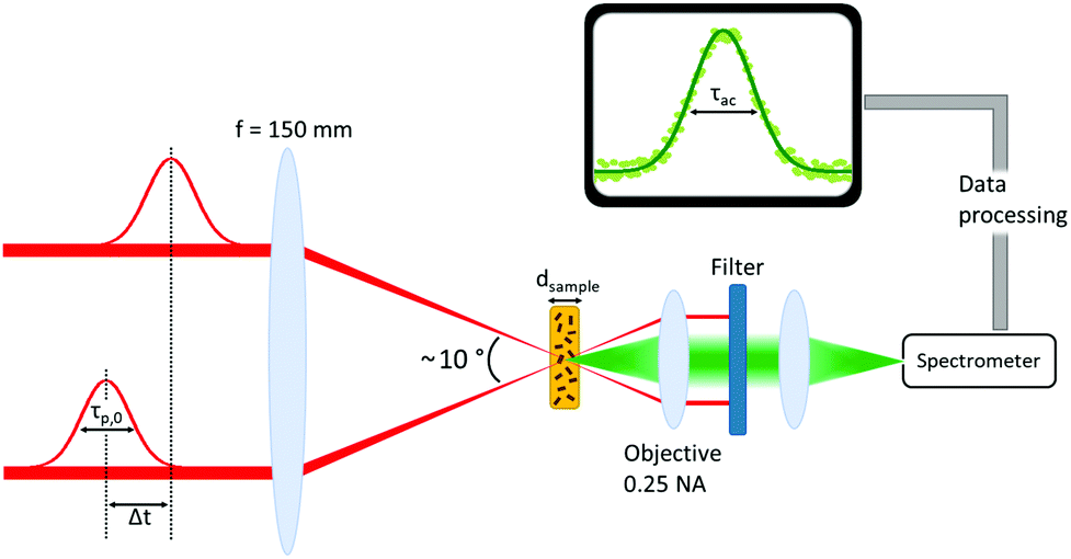 | ||
| Fig. 1 Measurement setup for acquisition of TPA (SHG) autocorrelation curves using a two beam scheme with relative delay. In case of SHG a BBO is used of the two photon absorber (CdSe platelets or CdS crystal). In the BBO case the objective is removed, since a collimated SHG beam is generated. | ||
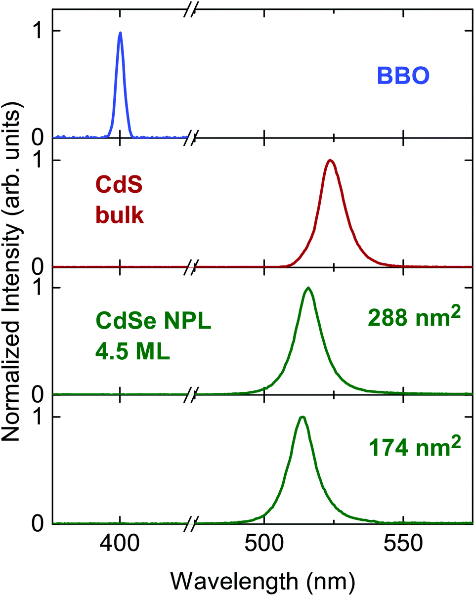 | ||
| Fig. 2 Normalized spectra resulting from second harmonic generation (blue), photoluminescence (PL) of CdS bulk (red) and PL of CdSe NPLs (green). In case of the semiconductor samples the emission is red-shifted with respect to SHG since the re-emission occurs at the bandgap wavelength. Spectra correspond to maximal temporal overlap of two 800 nm pulses within each sample. | ||
By definition the second order correlation function G(2)(t) in time is given by a temporal convolution of two pulse intensities IA(t) and IB(t).
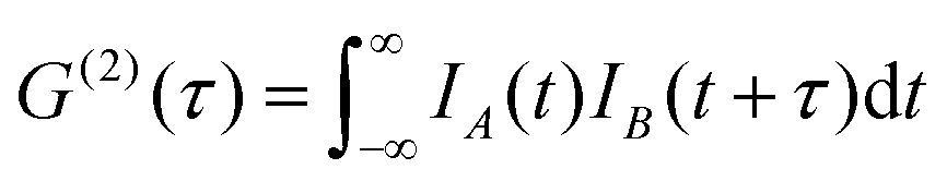 | (1) |
Fourier transformation (![[scr F, script letter F]](https://www.rsc.org/images/entities/char_e141.gif) ) allows to express this convolution also as a product in frequency domain. For Gaussian temporal pulses it can be shown that the FWHM τp of the pulse, is related to its autocorrelation width τacvia
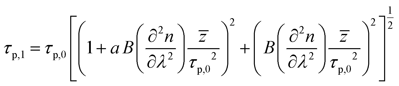
) allows to express this convolution also as a product in frequency domain. For Gaussian temporal pulses it can be shown that the FWHM τp of the pulse, is related to its autocorrelation width τacvia .43Fig. 3 shows the four resulting autocorrelation curves of our samples, which are listed in Table 1. We use a BBO crystal as an autocorrelation reference and define the relative deviation of the FWHM as Δ = |(τ − τBBO)/τBBO|, an indicator for the agreement among the different studied autocorrelation techniques. The deviation for the CdSe platelets is below 4%, thus giving excellent agreement with the BBO reference, while for the CdS bulk sample it is 9%, expectedly bigger due to considerable pulse broadening in CdS. Pulse broadening within the NPL samples due to dispersion can be shown to have no relevant effect in the two samples.44 This is the case because group velocity dispersion around 800 nm is low in polystyrene, the embedding matrix of the dispersed NPLs.45 The pulse broadening of an incoming pulse is given by:
 | (2) |
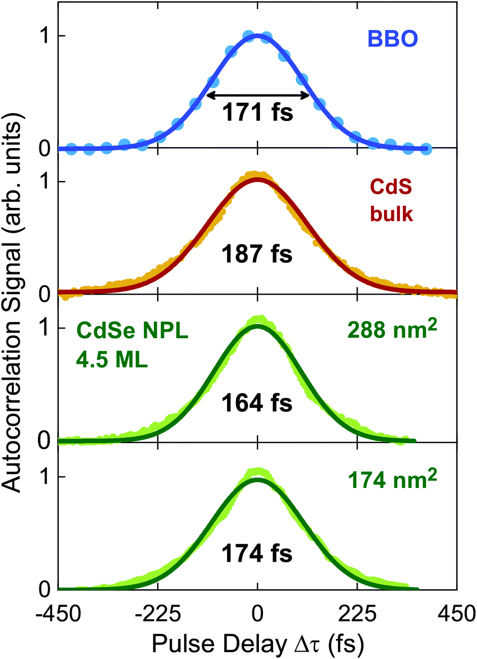 | ||
Fig. 3 Normalized autocorrelation curves resulting from different methods and samples, respectively vs. relative pulse delay in fs. Data were fitted assuming a Gaussian pulse shape, characteristic for the Coherent Mira 900 HP fs laser, as clearly seen for the BBO data. Autocorrelations are performed via SHG in BBO (blue), TPA in CdS bulk (red) and TPA in two different CdSe NPL samples (green) of distinct size via delaying one 800 nm beam vs. the other. The autocorrelation's FWHM is connected to the pulse FWHM τp by 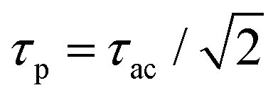 .43 The measured pulse width τp are indicated. .43 The measured pulse width τp are indicated. | ||
![[z with combining macron]](https://www.rsc.org/images/entities/i_char_007a_0304.gif) (eqn (2)) as well as parameter C
(eqn (2)) as well as parameter C
| CdSe NPL | ||||
|---|---|---|---|---|
| 174 nm2 | 288 nm2 | CdS | BBO | |
| τ p,1 (fs) meas. | 174 | 164 | 187 | 171 |
| τ p,1 (fs) est. | 174 | 174 | 191 | 171 |
| d sample (mm) | 0.95 | 0.90 | 0.50 | 0.50 |
|
(mm) |
0.49 | 0.57 | 0.50 | — |
| C (cm4 GW−2) | 41 | 76 | 4.2 × 10³ | — |
Here, τ0 and τ1 give the Gaussian pulse FWHM before and after passing the sample, is an effective emission depth within the sample and a is the (linear) chirp parameter. a is related to the instantaneous frequency ω(t) by ω(t) = ωc + dΦ/dt = ωc + 2at/τp,02 within our Gaussian pulse of central frequency ωc. B is a proportionality constant, given by B = (λ032![[thin space (1/6-em)]](https://www.rsc.org/images/entities/char_2009.gif) ln(2))/(πc02). The chirp parameter a relates to a spectral phase of a Gaussian pulse (chirp) and alters its time-bandwidth product.46 The pulse impinging on the sample is linearly chirped, as common for Ti:Sa laser systems, which are not bandwidth limited. a can be estimated from the time-bandwidth product of the laser source via
ln(2))/(πc02). The chirp parameter a relates to a spectral phase of a Gaussian pulse (chirp) and alters its time-bandwidth product.46 The pulse impinging on the sample is linearly chirped, as common for Ti:Sa laser systems, which are not bandwidth limited. a can be estimated from the time-bandwidth product of the laser source via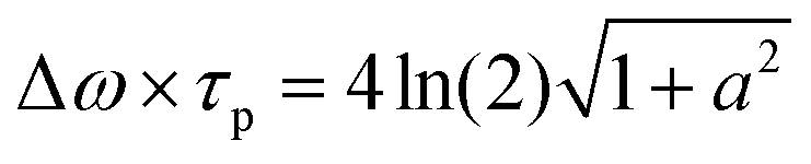 (with a = 1.7 for our laser system). Second, to calculate the effective emission depth , reabsorption during propagation of two-photon induced PL emission through the samples has to be considered. The effective emission depth due to reabsorption is calculated by:
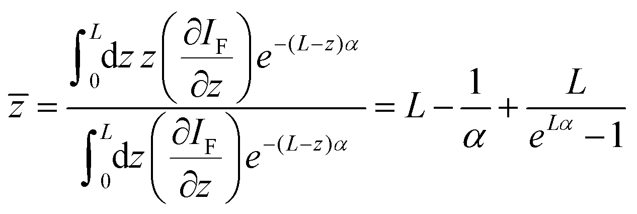 | (3) |
L gives the sample's thickness, IF the emission intensity and α represents the linear absorption coefficient. The relation above holds, as the Rayleigh length (2.5 mm) of the used 15 cm focussing lens for excitation is greater than the sample thickness (0.5 mm). The TPA induced luminescence emission per unit length (∂IF/∂z) and the incoming excitation wave's intensity Iexc (800 nm) are connected for TPA via:
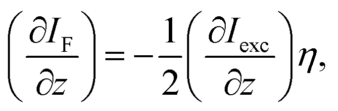 | (4) |
2.2. Power series and TPA cross section
Fig. 4 displays the excitation intensity dependent emission of the NPLs and CdS bulk. The observed linear behavior in the logarithmic presentation corresponds to a near quadratic intensity dependence. Beam A and B were switched on independently to acquire the two data sets. The unequal excitation intensities of Beam A and B, respectively, arise due to slight differences in the beam profiles at the same position. Influences from TPA saturation can be excluded, since in case of II–VI semiconductor nanocrystals a saturation intensity in the order of 200 GW cm−2 is expected,2 which translates to an average power of at least 60 W needed in our measurements, orders of magnitude higher as compared to our measurement range. Equally it has been shown, that for CdS bulk no saturation effects are observed below an excitation intensity of 6 GW cm−2.2,5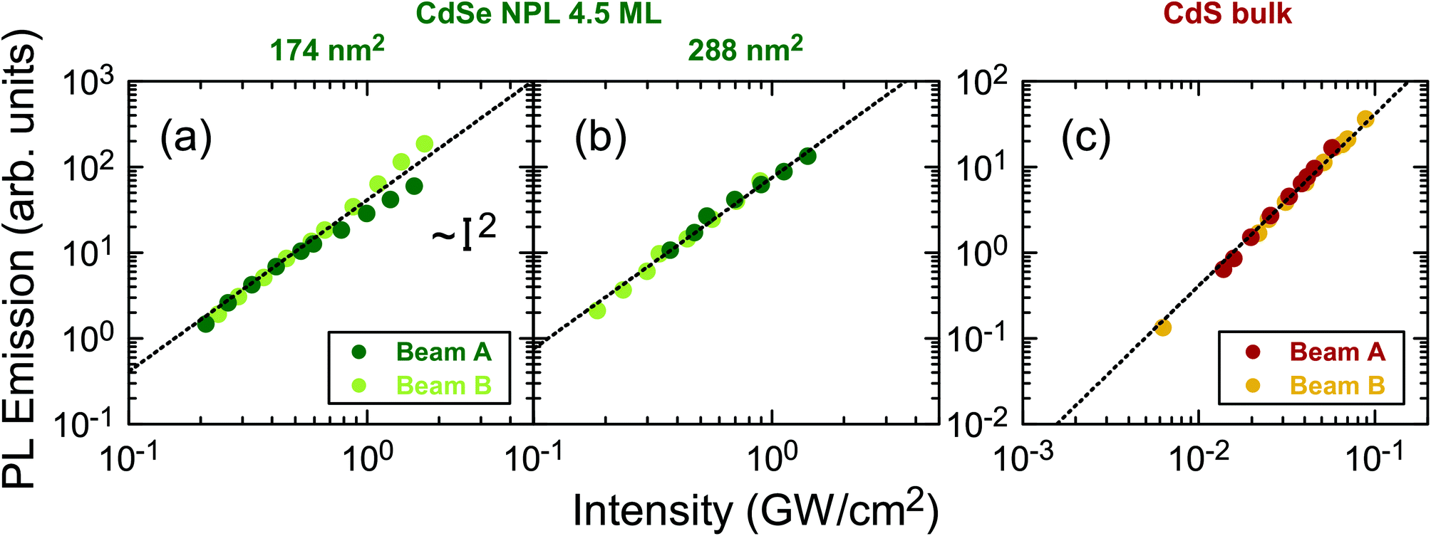 | ||
| Fig. 4 PL signal vs. the beam temporal and spatial peak intensity in GW cm−2 for NPLs of two different areas 174 nm2 (a) and 288 nm2 (b) as well as for CdS bulk (c). The quadratic fit according to eqn (5) (shown as a dotted fit line on the logarithmic scale) yields a factor C, the conversion figure of merit. | ||
To understand why CdSe NPLs are suitable for efficient second order autocorrelation, we target their TPA nonlinearity quantitatively in the next section. We use our intensity dependent measurements for TPA cross section calculation, which will demonstrate their considerably higher nonlinearity as compared to bulk. The acquired signal can be understood as the total emission intensity IF,out modified by an excitation and detection efficiency φ (a setup constant for each beam). Likewise, the signal S is proportional to the square of the incoming excitation wave's intensity Iexc.
| S(Iexc) = φIF,out = CIexc2 | (5) |
The conversion figure of merit C is directly obtained from fitting the data (Fig. 4) and used to retrieve the TPA cross section. The total number of PL photons leaving the sample, and hence the intensity IF,out, is diminished by reflection R (of the excitation) at the sample's front surface when entering and reflection of the emitted PL photons when exiting the sample.
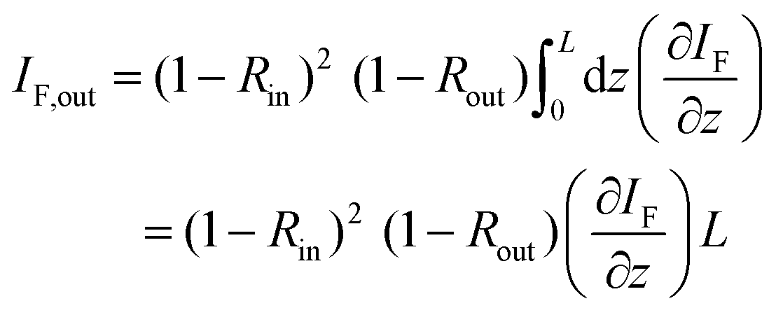 | (6) |
R = (n(λ) − 1)2/(n(λ) + 1)2 stands for the intensity reflection coefficient for entering or leaving the sample. They depend on the excitation and emission wavelength. Again, the derivative is linked to the attenuated excitation wave by the former introduced eqn (4). As the sample is transparent for the laser at 800 nm, no linear absorption is taken into account and the derivative of Iexc can be solely related to the TPA coefficient β by (∂Iexc/∂z) = −βIexc2. Using the eqn (4) and eqn (6) yields:
 | (7) |
Considering ϕ a system constant, it is possible to find β for a sample under test (s), once a reference (r) is known.
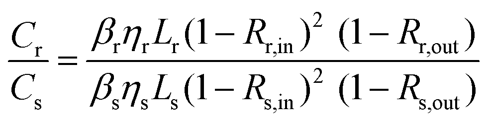 | (8) |
To apply eqn (8) for nanocrystalline materials, a relation between β and the particle TPA cross section σ(2) has to be used:
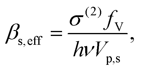 | (9) |
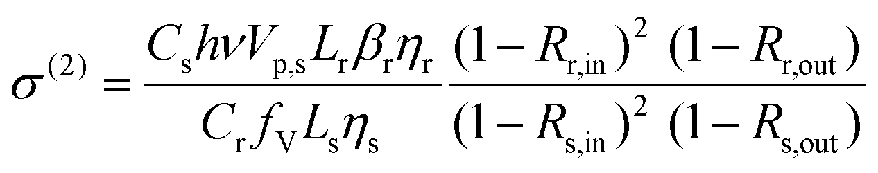 | (10) |
Taking CdS bulk as a reference (βr = 8.8 cm GW−1 (ref. 2)) and using eqn (10) with the results given in this work, TPA cross sections of 3.8 × 10⁶ GM (24 × 12 nm2 CdSe NPL) and 7.7 × 10⁵ GM (29 × 6 nm2 CdSe NPL) are obtained, considering the quantum yields η of the CdSe samples (both 15%) and reference (6.2%). We refer to ESI† for a detailed calculation. These results are in good agreement with the very high TPA cross sections obtained in z-scan and two-photon PLE in ref. 5 for platelets of comparable size. Hence the outcome substantiates that CdSe nanoplatelets with their extremely high nonlinearities are ideal to build high efficiency and low intensity pulse characterization autocorrelators. This will be addressed in the following.
For SHG to occur, e.g. in a BBO crystal, coherent interaction between the incoming photons is required as well as phase matching between the fundamental and generated second harmonic field. This requires critical angle or thermal phase matching (e.g. in birefringent media), periodically poled (pp)-crystals or very thin crystals, where walk off and phase lag are not limiting the performance. However, for broadband autocorrelation the crystals need to be thin due to group velocity dispersion and mismatch limiting the bandwidth. Hence materials with high nonlinearities are desired, as suggested in the introduction. Here TPA materials with high cross sections come into play, as they do not require phase matching of the fundamental and converted photons, since re-emission after two-photon excitation is spontaneous and incoherent so that there can be no back conversion of the generated radiation into the fundamental beam. As an example for the high efficiency we compare the efficiency of a very thin, dense 10 μm layer of nanoplatelets with 3.7 × 10⁶ GM (and assumed fill factor 100%) with a BBO of identical thickness at 10 GW cm−2 at 800 nm, typical power densities for a ∼100 MHz repetition rate, ∼100 fs Ti:Sa laser system, using ∼13 mW focused by a 0.2 NA objective. Due to the extremely thin crystal assumption the conversion efficiency is only ∼5 × 10⁻² % for the BBO, calculated using ref. 49 and taking into account that the Rayleigh length of the beam (>10 micron) is not smaller than the sample thickness. Estimating the TPA efficiency21 by φ = 1 − 1/(1 + βMatLIexc) up to 80% is feasible, given the parameters above. For the intrinsic TPA coefficient βMat of the NPLs itself, which allows comparison to bulk materials, we calculate βMat = 392 cm GW−1 for the larger 24 × 12 nm2 NPL and βMat = 122 cm GW−1 for the 29 × 6 nm2 NPL via βMat = βeff/fV from the obtained cross sections above viaeqn (9). Furthermore, using a luminescence quantum yield η of 15% for NPLs, the conversion total efficiency ![[small variant phi, Greek, tilde]](https://www.rsc.org/images/entities/i_char_e12c.gif) yields = φ × η = 12 %.
yields = φ × η = 12 %.
For our setup we were able to record autocorrelation traces down to <1 mW beam power. The sensitivity may be extended using a shorter focal length focusing lens, resulting in higher excitation power in the sample. However we did not use shorter lenses, to maintain our setup in a condition, where the sample length is smaller than the Rayleigh length of the lens, to be able to do quantitative referencing of TPA cross sections. The measurable range of input power is limited to below 200 GW cm−2 (60 W CW equivalent), the above mentioned TPA saturation intensity.
Contrasting the calculations for CdSe nanoplatelets and BBO we find, that the conversion efficiencies of such NPLs can exceed equivalent SHG in BBO by two orders of magnitude. In a similar manner, the efficiency of TPA autocorrelation in CdS bulk can be exceeded by about two orders, based of the enhancement of the two photon absorption coefficient in CdSe nanoplatelets relative to bulk (βr = 8.8 cm GW−1 (ref. 2)). In addition, oriented CdSe NPLs show directional PL emission in the z-direction.50 Hence, e.g. oriented multilayers can allow for high collection efficiency, for instance ideally matching a 0.4 NA detection optics.
It can be seen from the discussion above that autocorrelation with 2D semiconductors has higher efficiency, once very short interaction length is considered. Therefore TPA based autocorrelators have a great application potential for the characterization of ultrashort pulses. As the two-photon absorption spectrum is broad,5i.e. very high bandwidth (>100 nm), few fs pulses may be autocorrelated efficiently opening up great application perspectives. The performance of TPA autocorrelation with nanoplatelets in terms of efficiency for wavelength different than 800 nm or for large spectral bandwidth follows from the spectral course of TPA cross sections for CdSe nanoplatelets, measured in ref. 5.
Reasoned in the ultra strong electronic confinement, the very high TPA cross sections result in superiority of nanoplatelets over bulk semiconductor materials for autocorrelation, used in the past. Many of the discussed semiconductors were limited to a wavelength regime above 1 micron and were also quickly reaching intensity saturation limits for intense beams.40 All these obstacles are not present with nanoplatelets, yielding high sensitivity and no saturation effects. Instead of detecting the luminescence externally, our NPLs can possibly be used in on-chip photonics, combining the large nonlinearities and resulting high sensitivities with direct detection of the two photon induced luminescence. For example nanoplatelets can be deposited on a planar photodiode, which detects the autocorrelation related PL with high efficiency. Especially due to the fact, that this PL emission is directional,50 and mainly in the direction of the surface normal of nanoplatelets such a structure will provide high efficiency. Advances towards the processing and characterization of quantum confined CdSe particles in optoelectronics have already been made.51,52 We also remark that conventional (epitaxial) II–VI quantum wells will not be able to compete with these structures, as due to e.g. interface roughness scattering the exciton coherence areas (volumina) do not reach the platelet values, resulting presumably in considerably lower nonlinearities and hence autocorrelation efficiencies. Further, as in such epitaxial structures the dielectric mismatch between the CdSe quantum well and surrounding (e.g. ZnxCd1−xSe) material is low, the excitonic correlation is considerably lower and therefore the exciton Bohr radius is higher. This results in lower transition dipole moments,21 concatenated for the two photon transition, and due to second order Fermi's Golden Rule in considerably smaller TPA rates. We remark that the efficiency of autocorrelation can be further enhanced considerably by using larger nanoplatelets as the ones used in this study. Their TPA cross sections can be with ∼108 GM (ref. 5) even a hundred times higher, further enhancing the autocorrelation efficiency. Hence II–VI nanoplatelets are a favored system for TPA based autocorrelation.
3. Conclusion
We have shown that CdSe nanoplatelets can be used for a new class of semiconductor broadband autocorrelators with unprecedented sensitivity. Collecting two-photon induced fluorescence, we measured pulse durations of fs laser pulses using different CdSe NPLs and a CdS bulk sample. We obtained very good agreement of the TPA based methods with conventional BBO based SHG pulse width measurements. In addition, we have demonstrated very high two-photon absorption cross sections and saturation intensities, which are related to strong anisotropic confinement and in-plane wave function coherence in CdSe nanoplatelets. They lead to very high autocorrelation efficiencies, which can be two orders of magnitude higher as conventional techniques, especially for short interaction length. Apart from the exceptional sensitivity, a main advantage, however, is the large potential cross- and auto correlation bandwidth allowing autocorrelation of (<10) fs pulses. The total efficiency could be further boosted if e.g. larger nanoplatelets are used or the nanoplatelets are deposited directly atop a planar photodiode, so that all PL is detected via the photodiode. This diode should have higher bandgap than the fundamental laser pulses, but lower than the emitted PL. In such a scheme the high nonlinearity of nanoplatelets could be combined with even higher detection efficiency. Also the nanoplatelets can by synthesiszed from many II–VI material combinations, so that a broad range of spectral regions for autocorrelation can be accessed.4. Methods
CdSe nanoplatelets50 of 4.5 ML thickness and 24 × 12 nm2 and 29 × 6 nm2 lateral size were dispersed in a polystyrene (PS) matrix as follows: In a vessel, 1 g of PS beads were mixed with 4 mL of toluene and heated to 60 °C while stirring. After 2 h, the solution was left to cool to room temperature. Subsequently, CdSe NPLs dispersed in hexane were mixed with the PS solution and left to dry at room temperature to produce the CdSe NPL-doped PS film. Details of the CdSe NPL synthesis are described in ref. 53. Size and shape of the NPLs were determined by TEM. See also ESI† for further details. A hexagonal CdS wafer (0.5 mm thickness) with c-axis perpendicular to the surface ((0001) orientation) is used as a two photon autocorrelation reference. For our autocorrelation measurements the beam of a 171 fs Titan-Sapphire-Laser (Coherent Mira-HP) operated at 800 nm was split into two parts and both focused onto the sample in a symmetric, but non-collinear geometry with a relative angle of ∼10°. The geometry is shown in Fig. 1. In case of SHG autocorrelation via a 0.5 mm BBO crystal, the phase matching angle was found via optimizing the generated SHG, coupled via a lens to a spectrometer. To autocorrelate the pulses in case of the CdS and CdSe samples, the fluorescence was collected by a 0.25 NA objective and focused on the entrance slit of a BW&TEk BRC111A spectrometer.Conflicts of interest
There are no conflicts of interest to declare.Acknowledgements
A. W. A. acknowledges funding by DFG project number AC290-2/1. Additionally, this project has received funding from the European Research Council (ERC) under the European Union's Horizon 2020 research and innovation program (I. M., grant agreement no. 714876 PHOCONA).References
- S. A. Blanton, M. A. Hines, M. E. Schmidt and P. Guyot-Sionnest, J. Lumin., 1996, 70, 253–268 CrossRef CAS.
- J. He, J. Mi, H. Li and W. Ji, J. Phys. Chem. B, 2005, 109, 19184–19187 CrossRef CAS.
- X. Feng and W. Ji, Opt. Express, 2009, 17, 13140 CrossRef CAS PubMed.
- X. Li, J. van Embden, J. W. M. Chon and M. Gu, Appl. Phys. Lett., 2009, 94, 103117 CrossRef.
- R. Scott, A. W. Achtstein, A. Prudnikau, A. Antanovich, S. Christodoulou, I. Moreels, M. Artemyev and U. Woggon, Nano Lett., 2015, 15, 4985–4992 CrossRef CAS PubMed.
- M. Allione, A. Ballester, H. Li, A. Comin, L. Movilla, J. I. Climente, I. Moreels and L. Manna, ACS Nano, 2013, 7, 2443–2452 CrossRef CAS PubMed.
- A. W. Achtstein, A. Ballester, J. L. Movilla, J. Hennig, J. I. Climente, A. Prudnikau, A. Antanovich, R. Scott, M. V. Artemyev, J. Planelles and U. Woggon, J. Phys. Chem. C, 2015, 119, 1260–1267 CrossRef CAS.
- G. L. Dakovski and J. Shan, J. Appl. Phys., 2013, 114, 014301 CrossRef.
- A. W. Achtstein, J. Hennig, A. Prudnikau, M. V. Artemyev and U. Woggon, J. Phys. Chem. C, 2013, 117, 25756–25760 CrossRef CAS.
- M. Nyk, J. Szeremeta, D. Wawrzynczyk and M. Samoc, J. Phys. Chem. C, 2014, 118, 17914–17921 CrossRef CAS.
- J. Heckmann, R. Scott, A. V. Prudnikau, A. Antanovich, N. Owschimikow, M. Artemyev, J. I. Climente, U. Woggon, N. B. Grosse and A. W. Achtstein, Nano Lett., 2017, 17, 6321–6329 CrossRef CAS PubMed.
- E.-S. Wu, J. H. Strickler, W. R. Harrell and W. W. Webb, Optical/Laser Microlithography V, 1992 Search PubMed.
- B. Guzelturk, Y. Kelestemur, M. Olutas, S. Delikanli and H. V. Demir, ACS Nano, 2014, 8, 6599–6605 CrossRef CAS PubMed.
- C. She, I. Fedin, D. S. Dolzhnikov, A. Demortière, R. D. Schaller, M. Pelton and D. V. Talapin, Nano Lett., 2014, 14, 2772–2777 CrossRef CAS PubMed.
- M. Li, M. Zhi, H. Zhu, W.-Y. Wu, Q.-H. Xu, M. H. Jhon and Y. Chan, Nat. Commun., 2015, 8513 CrossRef CAS PubMed.
- R. Schropp, J. de Wild, W. van Sark, A. Meijerink, J. Feenstra and J. Schermer, Materials Challenges in Alternative & Renewable Energy (MCARE 2016); Symposium 2: Spectral Conversion Materials for Energy Applications; S2-001 April 18, 2016, 2016.
- E. Petryayeva, W. Russ Algar and I. L. Medintz, Appl. Spectrosc., 2013, 67, 215–252 CrossRef CAS PubMed.
- F. Wang, D. Banerjee, Y. Liu, X. Chen and X. Liu, Analyst, 2010, 135, 1839–1854 RSC.
- V. Biju, T. Itoh, A. Abdulaziz, A. Sujith and M. Ishikawa, Anal. Bioanal. Chem., 2008, 391, 2469–2495 CrossRef CAS PubMed.
- K.-L. Chou, N. Won, J. Kwag, S. Kim and J.-Y. Chen, J. Mater. Chem. B, 2013, 1, 4584 RSC.
- J. Planelles, A. W. Achtstein, R. Scott, N. Owschimikow, U. Woggon and J. I. Climente, ACS Photonics, 2018, 5, 3680–3688 CrossRef CAS.
- A. W. Achtstein, R. Scott, S. Kickhöfel, S. T. Jagsch, S. Christodoulou, G. H. Bertrand, A. V. Prudnikau, A. Antanovich, M. Artemyev, I. Moreels, A. Schliwa and U. Woggon, Phys. Rev. Lett., 2016, 116, 116802 CrossRef PubMed.
- A. W. Achtstein, A. Schliwa, A. Prudnikau, M. Hardzei, M. Artemyev, C. Thomsen and U. Woggon, Nano Lett., 2012, 12, 3151–3157 CrossRef CAS PubMed.
- S. Ithurria and B. Dubertret, J. Am. Chem. Soc., 2008, 130, 16504–16505 CrossRef CAS PubMed.
- A. Antanovich, A. W. Achtstein, A. Matsukovich, A. Prudnikau, P. Bhaskar, V. Gurin, M. Molinari and M. Artemyev, Nanoscale, 2017, 9, 18042–18053 RSC.
- A. W. Achtstein, O. Marquardt, R. Scott, M. Ibrahim, T. Riedl, A. V. Prudnikau, A. Antanovich, N. Owschimikow, J. K. N. Lindner, M. Artemyev and U. Woggon, ACS Nano, 2018, 12, 9476–9483 CrossRef CAS PubMed.
- J. Q. Grim, S. Christodoulou, F. Di Stasio, R. Krahne, R. Cingolani, L. Manna and I. Moreels, Nat. Nanotechnol., 2014, 9, 891–895 CrossRef CAS PubMed.
- R. Scott, A. V. Prudnikau, A. Antanovich, S. Christodoulou, T. Riedl, G. H. V. Bertrand, N. Owschimikow, J. K. N. Lindner, Z. Hens, I. Moreels, M. Artemyev, U. Woggon and A. W. Achtstein, Nanoscale, 2019, 11, 3958–3967 RSC.
- J. F. Specht, R. Scott, M. Corona Castro, S. Christodoulou, G. H. V. Bertrand, A. V. Prudnikau, A. Antanovich, L. D. A. Siebbeles, N. Owschimikow, I. Moreels, M. Artemyev, U. Woggon, A. W. Achtstein and M. Richter, Nanoscale, 2019, 11, 12230–12241 RSC.
- Y. Takagi, T. Kobayashi, K. Yoshihara and S. Imamura, Opt. Lett., 1992, 17, 658–660 CrossRef CAS PubMed.
- H. K. Tsang, L. Y. Chan, J. B. D. Soole, H. P. LeBlanc, M. A. Koza and R. Bhat, Electron. Lett., 1995, 31, 1773–1775 CrossRef CAS.
- Y. Takagi, Appl. Opt., 1994, 33, 6328–6332 CrossRef CAS PubMed.
- F. R. Laughton, J. Marsh, D. Barrow and E. Portnoi, IEEE J. Quantum Electron., 1994, 30, 838–845 CrossRef CAS.
- L. Barry, P. Bollond, J. Dudley, J. Harvey and R. Leonhardt, Electron. Lett., 1996, 32, 1922–1923 CrossRef CAS.
- J. K. Ranka, A. L. Gaeta, A. Baltuska, M. S. Pshenichnikov and D. A. Wiersma, Opt. Lett., 1997, 22, 1344–1346 CrossRef CAS PubMed.
- W. Rudolph, M. Sheik-Bahae, A. Bernstein and L. F. Lester, Opt. Lett., 1997, 22, 313–315 CrossRef CAS PubMed.
- Z. Zheng, A. M. Weiner, J. H. Marsh and M. M. Karkhanehchi, IEEE Photonics Technol. Lett., 1997, 9, 493–495 Search PubMed.
- N. F. Kleimeier, T. Haarlammert, H. Witte, U. Schühle, J.-F. Hochedez, A. BenMoussa and H. Zacharias, Opt. Express, 2010, 18, 6945–6956 CrossRef CAS PubMed.
- D. T. Reid, M. Padgett, C. McGowan, W. E. Sleat and W. Sibbett, Opt. Lett., 1997, 22, 233–235 CrossRef CAS PubMed.
- D. Reid, W. Sibbett, J. Dudley, L. Barry, B. Thomsen and J. Harvey, Appl. Opt., 1998, 37, 8142–8144 CrossRef CAS.
- B. V. Emmanuel Rosencher, Optoelectronics, Cambridge Univ. Press, 2002 Search PubMed.
- M. Hassan, A. Wirth, I. Grguras, T. T. Luu, A. Moulet, V. Yakovlev, J. Gagnon, O. Razskazovskaya, R. Santra, S. Pabst, A. Azzeer, Z. Alahmed, V. Pervak, F. Krausz and E. Goulielmakis, Attosecond physics with Synthesized Transients of Light, 2012, p. LW4H.2 Search PubMed.
- J.-C. Diels and W. Rudolph, Ultrashort Laser Pulse Phenomena, Academic Press, Burlington, 2nd edn, 2006, pp. 457–489 Search PubMed.
- G. Agrawal, Nonlinear Fiber Optics, Academic Press, Boston, 5th edn, 2013, pp. 57–85 Search PubMed.
- N. Sultanova, S. Kasarova and I. Nikolov, Acta Phys. Pol., A, 2009, 116, 585–587 CrossRef CAS.
- J.-C. Diels and W. Rudolph, Ultrashort Laser Pulse Phenomena (Second Edition), Academic Press, Burlington, 2nd edn, 2006, pp. 1–60 Search PubMed.
- G. He, Nonlinear Optics and Photonics, Oxford Univ. Press, 2014 Search PubMed.
- Z. Hens and I. Moreels, J. Mater. Chem., 2012, 22, 10406–10415 RSC.
- R. W. Boyd, Nonlinear Optics, Academic Press, Burlington, 3rd edn, 2008 Search PubMed.
- R. Scott, J. Heckmann, A. V. Prudnikau, A. Antanovich, A. Mikhailov, N. Owschimikow, M. Artemyev, J. I. Climente, U. Woggon, N. B. Grosse and A. W. Achtstein, Nat. Nanotechnol., 2017, 1155–1160 CrossRef CAS PubMed.
- X. Geng, L. Niu, Z. Xing, R. Song, G. Liu, M. Sun, G. Cheng, H. Zhong, Z. Liu, Z. Zhang, L. Sun, H. Xu, L. Lu and L. Liu, Adv. Mater., 2010, 22, 638–642 CrossRef CAS PubMed.
- A. Robin, E. Lhuillier, X. Z. Xu, S. Ithurria, H. Aubin, A. Ouerghi and B. Dubertret, Sci. Rep., 2016, 6, 24909 CrossRef CAS PubMed.
- G. H. V. Bertrand, A. Polovitsyn, S. Christodoulou, A. H. Khan and I. Moreels, Chem. Commun., 2016, 52, 11975–11978 RSC.
Footnotes |
| † Electronic supplementary information (ESI) available. See DOI: 10.1039/C9NR06156H |
| ‡ These authors contributed equally to this work. |
| This journal is © The Royal Society of Chemistry 2019 |