
Polarization-dependent electric potential distribution across nanoscale ferroelectric Hf0.5Zr0.5O2 in functional memory capacitors†
Yury
Matveyev
 *ab,
Vitalii
Mikheev
b,
Dmitry
Negrov
b,
Sergei
Zarubin
b,
Abinash
Kumar
c,
Everett D.
Grimley
c,
James M.
LeBeau
c,
Andrei
Gloskovskii
a,
Evgeny Y.
Tsymbal
*db and
Andrei
Zenkevich
*b
*ab,
Vitalii
Mikheev
b,
Dmitry
Negrov
b,
Sergei
Zarubin
b,
Abinash
Kumar
c,
Everett D.
Grimley
c,
James M.
LeBeau
c,
Andrei
Gloskovskii
a,
Evgeny Y.
Tsymbal
*db and
Andrei
Zenkevich
*b
aDeutsches Elektronen-Synchrotron, 85 Notkestraße, Hamburg, D-22607, Germany
bMoscow Institute of Physics and Technology, 9, Institutskiy lane, Dolgoprudny, Moscow region, 141700, Russia. E-mail: yury.matveev@desy.de; zenkevich.av@mipt.ru; tsymbal@unl.edu
cDepartment of Materials Science and Engineering, North Carolina State University, Raleigh, NC 27606, USA
dDepartment of Physics and Astronomy, University of Nebraska-Lincoln, Lincoln, NE 68588, USA
First published on 10th October 2019
Abstract
The emergence of ferroelectricity in nanometer-thick films of doped hafnium oxide (HfO2) makes this material a promising candidate for use in Si-compatible non-volatile memory devices. The switchable polarization of ferroelectric HfO2 controls functional properties of these devices through the electric potential distribution across the capacitor. The experimental characterization of the local electric potential at the nanoscale has not so far been realized in practice. Here, we develop a new methodology which allows us, for the first time, to experimentally quantify the polarization-dependent potential profile across few-nanometer-thick ferroelectric Hf0.5Zr0.5O2 thin films. Using a standing-wave excitation mode in synchrotron based hard X-ray photoemission spectroscopy, we depth-selectively probe TiN/Hf0.5Zr0.5O2/W prototype memory capacitors and determine the local electrostatic potential by analyzing the core-level line shifts. We find that the electric potential profile across the Hf0.5Zr0.5O2 layer is non-linear and changes with in situ polarization switching. Combined with our scanning transmission electron microscopy data and theoretical modeling, we interpret the observed non-linear potential behavior in terms of defects in Hf0.5Zr0.5O2, at both interfaces, and their charge state modulated by the ferroelectric polarization. Our results provide an important insight into the intrinsic electronic properties of HfO2 based ferroelectric capacitors and are essential for engineering memory devices.
1. Introduction
Fast write speed, high-density and low-power consumption non-volatile memories, which would allow retaining information when the power is switched off, are highly desirable for modern computing technologies. Among different concepts of such memories, ferroelectric random access memories (FeRAM) appear to be competitive, where the information is stored through the direction of remnant polarization. In particular, in a ferroelectric field-effect transistor (FeFET) memory device, the polarization direction of a ferroelectric gate affects the threshold voltage controlling the electric current in the transistor channel.1,2 In an alternative ferroelectric memory concept called ferroelectric tunnel junction (FTJ),3–5 an ultrathin ferroelectric barrier is sandwiched between two conducting electrodes with different work functions and/or screening lengths. The tunnelling current is strongly dependent on ferroelectric polarization orientation yielding a large tunnel electroresistance (TER) ratio due to changes in the electrostatic potential profile controlling the tunnelling current. Both memory concepts allow for a non-destructive readout, and the combination of functional characteristics potentially makes such ferroelectric devices promising candidates for “universal” memory combining high speed, non-volatility, and scalability down to the nanometer range. Indeed, the implementation of both FeFETs [e.g., ref. 6–8] and FTJs has been reported previously [e.g., ref. 9–13] and showed their potential as memory devices. Unfortunately, commercialization of these devices is hindered by the problems arising from the use of conventional perovskite ferroelectrics due to their poor compatibility with the Si-based CMOS technology.Recently, ferroelectricity has been discovered in doped or alloyed HfO2 thin films.14 The advantage of this class of ferroelectric materials over perovskites is their perfect compatibility with the modern CMOS technology. The ferroelectric properties of HfO2 have been assigned to the non-centrosymmetric orthorhombic phase (space group Pca21).14,15 This structural phase is metastable and crystallizes upon high-temperature annealing in thin films with thicknesses on the order of nanometers to tens of nanometers depending on the type of dopants and their concentration, film thickness, conditions of thermal treatment and the type of electrodes.15–18 Following the discovery of ferroelectricity in HfO2, its applicability as a functional gate oxide in nanoscale FeFET memory devices has been successfully demonstrated.7,8,19 It should be noted that the temperature required for HZO to crystallize in the ferroelectric phase (T ∼ 400 °C) is significantly lower compared to the other types of doped HfO2. This feature makes HZO films advantageous for the back-end-of-line fabrication of nonvolatile memory devices. Indeed, the realization of the first CMOS-compatible FTJs based on a ferroelectric HZO barrier layer has recently been reported.20 However, the functional properties of both HfO2 based FeFET and FTJ prototypic memory devices obtained so far still need significant improvement in order to have chances for their commercialization.
An important role in the performance of both types of ferroelectric memory devices is played by the electrostatic potential, which dynamically changes in the process of memory operation. The potential profile is controlled by ferroelectric polarization as well as by electronic and structural properties of the ferroelectric layer and boundary conditions at the interfaces with metal electrodes. By proper engineering of the electrostatic potential profile across a ferroelectric HfO2 layer it is feasible to enhance the memory performance. To this end, it is critical to develop a methodology for the quantitative characterization of the electrostatic potential in the nanoscale ferroelectric devices.
Previously, X-ray photoemission spectroscopy (XPS) was used to derive the electronic band alignment at the metal/ferroelectric interfaces of BaTiO3![[thin space (1/6-em)]](https://www.rsc.org/images/entities/char_2009.gif) 13 and HZO20 layers for a fixed polarization orientation intrinsically acquired by the ferroelectric. At the same time, it was shown that the laboratory XPS analysis can be employed to monitor the effect of polarization reversal in bulk BaTiO3 following in situ deposition of a metal overlayer.21 By combining the spectroscopic measurements with in situ electrical biasing, the study of polarization and electric-field induced effects on the electronic structure of the interface between metal and bulk ferroelectric PMN-PT was performed.22 Recently, we used synchrotron-based hard X-ray photoemission spectroscopy (HAXPES) in operando to quantify polarization dependent conduction band offsets at interfaces in ferroelectric TiN/HZO/TiN capacitors.23 With a tunable energy range of 5–12 keV, this technique enables probing layers down to about 20 nm beneath the surface. This approach allows for a non-destructive characterization of the interface properties in the functional ferroelectric capacitors. In addition, by using a so-called X-ray standing-wave (SW) excited mode in HAXPES,24 the elemental depth profile, interface properties, and the polarization-induced built-in electric potentials at interfaces, particularly, in the LCO/STO superlattices, were recently determined.25
13 and HZO20 layers for a fixed polarization orientation intrinsically acquired by the ferroelectric. At the same time, it was shown that the laboratory XPS analysis can be employed to monitor the effect of polarization reversal in bulk BaTiO3 following in situ deposition of a metal overlayer.21 By combining the spectroscopic measurements with in situ electrical biasing, the study of polarization and electric-field induced effects on the electronic structure of the interface between metal and bulk ferroelectric PMN-PT was performed.22 Recently, we used synchrotron-based hard X-ray photoemission spectroscopy (HAXPES) in operando to quantify polarization dependent conduction band offsets at interfaces in ferroelectric TiN/HZO/TiN capacitors.23 With a tunable energy range of 5–12 keV, this technique enables probing layers down to about 20 nm beneath the surface. This approach allows for a non-destructive characterization of the interface properties in the functional ferroelectric capacitors. In addition, by using a so-called X-ray standing-wave (SW) excited mode in HAXPES,24 the elemental depth profile, interface properties, and the polarization-induced built-in electric potentials at interfaces, particularly, in the LCO/STO superlattices, were recently determined.25
In this paper, we report on the application of SW-HAXPES technique to study in operando the prototype of memory devices. Since such devices usually comprise polycrystalline rather than epitaxial layers with characteristic thicknesses in ∼10 nm range, the use of “classic” X-rays standing wave, excited by the interference of Braggs reflections from single crystals, is limited. Therefore, we have implemented the so-called near-total reflection (NTR) X-ray standing wave excitation mode, where the SWs are formed by the interference of X-rays incident at a glancing angle and reflected from the engineered bottom layer comprising heavy atoms. This technique was previously used to determine the depth resolved charge accumulation at the ferroelectric layer (BiFeO3) in contact with a doped Mott insulator (Ca1−xCexMnO3).26
Using NTR-SW HAXPES we depth-selectively probe the local electrostatic potential across nanoscale ferroelectric HZO layer in functional TiN/HZO/W prototype memory capacitors by measuring the kinetic energy of photoelectrons and subsequent core-line shifts of HZO constituents. Furthermore, in situ electric biasing of the sample allows us to directly monitor the effect of ferroelectric polarization switching on the potential profile. The experimentally determined non-linear polarization-dependent potential across ferroelectric HZO reveals the presence of space charges in a sub-nm-thick layer close to both interfaces, which effectively screen the depolarizing electric field. Based on our electrostatic modelling with realistic parameters, we attribute charges at the top interface to oxygen vacancies in hafnia originating from the redox reaction at the TiN/HZO interface, in agreement with the angular-dependent photoemission spectra analysis. HAADF STEM is employed to characterize the atomic-scale structure of the HZO layer in the TiN/HZO/W capacitors which reveals structural distortions of HZO at the HZO/W interface, which hints at the origin of the charged defects there.
2. Experimental
The samples were grown on Si chips 1.5 × 1.5 cm2 in size. Firstly, the 50 nm-thick W layer was deposited by magnetron sputtering. On top of this layer Hf0.5Zr0.5O2 (HZO) layer 9 nm in thickness was grown by atomic layer deposition (ALD) on top. The HZO growth process has been described in detail previously.23,27 A TiN overlayer was deposited by magnetron sputtering at the optimized thickness d ∼ 10 nm to ensure continuous film coverage, sufficient conductivity and reasonably high yield of photoelectrons from the buried interfaces. In order to stabilize the non-centrosymmetric orthorhombic phase, the as-grown structures were exposed to rapid thermal annealing at T = 400 °C. Thus formed tri-layers were patterned into functional ferroelectric capacitor devices with lateral dimensions 150 × 3000 μm2 chosen to match the X-ray beam footprint at P09 beamline at DESY. To ensure the ability of in situ pulsed switching and polarization measurements from the remote source-meter unit the metal pads ∼0.25 mm2 in size connected to capacitor electrodes were also fabricated on the chip. More details are provided in ESI section S1.†The ferroelectric properties of the fabricated TiN/Hf0.5Zr0.5O2/W capacitors were examined upon the growth ex situ using Cascade Summit 1100 probe station coupled with Agilent semiconductor device analyzer B1500A and in situ during HAXPES analysis with Agilent B2912A source-measure unit. In both cases, the positive-up negative-down (PUND) technique was utilized (see ESI section S2†).
Operando HAXPES measurements were performed at the beamline P09 of PETRA III (DESY) with Specs 225 HV analyzer choosing an excitation energy E = 6 keV with an overall energy resolution of about 0.2 eV.28 The spectra were acquired in short-circuit configurations, with both electrodes kept grounded. The acquisition of spectra always started upon ∼10 min after switching voltage pulses in order to obtain the true steady-state conditions. The sample angle with respect to the beam was controlled by monitoring the relative positions of direct and partially reflected beam with Pilatus 100 K detector system placed behind the sample. First, four regions of interest at the incidence angle 3° were acquired: W 4d, Hf 3d5/2, Hf 4f and Ti 2p. The O 1s spectrum was found consisting of multiple components originating from the different layers in our structure (ESI section S5.1†). Later, for each polarization direction, only Hf 3d5/2, Hf 4f and Ti 2p spectral lines were acquired at 20 different angles in the range from 0.35 to 1.05 degrees.
HAADF-STEM imaging was performed on a FEI Titan G2 60–300 kV equipped with a probe-corrector operated at 200 kV with a beam current of 60 pA and probe semi-convergence angle ≈19.6 mrad. The collection inner semi-angle was 77 mrad. Drift and scan-coil distortion correction has been applied to the atomically resolved images using the RevSTEM based approach.29 Atom column spacing maps were generated by fitting the atom columns to 2D Gaussian distributions via a custom Python script.
3. Results and discussion
In the HAXPES experiment, a standing wave is generated by interference of the incident monochromatic X-ray beam with photons reflected from the bottom metal layer close to total external reflection condition. By changing the incidence angle, one can shift the position of the standing-wave maximum, thus allowing a depth-selective scan across the ferroelectric layer. The electric potential profile is obtained by measuring the energy spectra of emitted photoelectrons associated with the core levels of the elements comprising the capacitor. Changing the incidence angle of the X-ray beam and thus the position of the standing-wave maximum results in a shift of the core-level spectrum, which reflects the local potential at the point corresponding to the maximum intensity of the standing wave. Thus, by measuring the core-level spectra at different incidence angles one can reconstruct the electric potential profile across the ferroelectric layer. We note that the observed shifts are not related to the dynamic charging effect of the HZO since no shifts were observed while continuously measuring at the fixed incidence angle (for details, see ESI section S4†).We employ this technique to measure an electric potential across functional TiN/HZO/W capacitors. Fig. 1a shows the general experimental layout for the HAXPES standing-wave measurements. Here an X-ray beam is incident at a glancing angle on the surface of the ferroelectric capacitor. Depending on the angle of incidence, the maximum intensity of the standing wave appears at a different depth within the HZO layer. This behavior is illustrated in Fig. 1b, where the local X-ray intensity distribution across a TiN(10 nm)/HZO(9 nm)/W(50 nm) capacitor as a function of the angle of incidence is modelled using the parameters of the sample (ESI sections S5.3–5.5†). The appearance of the maximum standing-wave intensity at different depths enables selective probing of a specific region within the sample by measuring the core-level spectra of emitted photoelectrons.
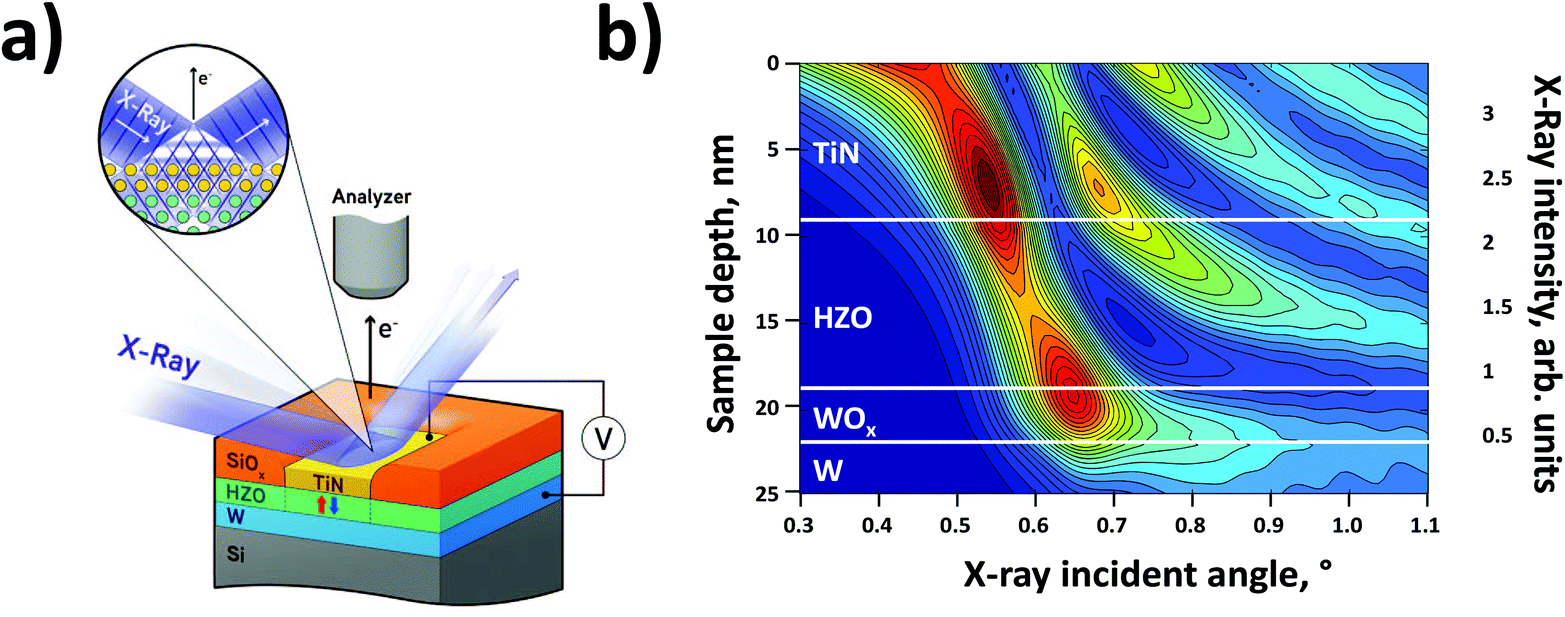 | ||
| Fig. 1 (a) Schematic view of operando standing-wave HAXPES experiment on TiN/HZO/W FE devices; (b) simulated local X-ray intensity distribution map across a TiN(10 nm)/Hf0.5Zr0.5O2(10 nm)/W(50 nm) capacitor as a function of incident angle. | ||
The remnant polarization of the ferroelectric capacitor device used in HAXPES analysis is determined in situ by the pulsed switching technique known as PUND (positive-up negative-down;30 see ESI section S2†). The typical ferroelectric response is illustrated by the polarization–voltage curve shown in Fig. S2,† which yields a remnant polarization P ≈ 16.5 μC cm−2. HAXPES spectra are acquired upon about 20 polarization switching cycles to “wake-up” the devices (ESI section S3†). Fig. 2a–c shows typical photoemission spectra of the Ti 2p, Hf 4f and W 4d5/2 core-level lines, acquired for the particular incident X-ray angle θ = 3° with respect to the sample surface and normally emitted photoelectrons. These spectra demonstrate the possibility of obtaining the required spectroscopic information from the whole capacitor stack at the employed experimental conditions.
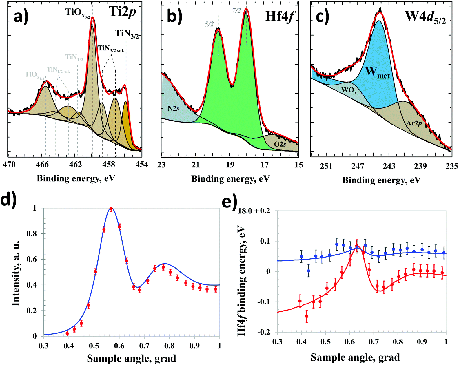 | ||
| Fig. 2 The Hf 4f (a), Ti 2p (b) and W4 d5/2 (c) core-level lines collected at the X-ray incidence angle θ = 3 grad (each spectrum is represented by several components, Ar 2p peak arises from the residual Ar in magnetron sputtered TiN and W layers). The Hf 4f7/2 line intensity (d) and position (e) as a function of X-ray beam incident angle: circles – experimental points, lines – fit; blue – polarization “up”, red – polarization “down”. | ||
Fig. 2d and e show, respectively, the Hf 4f7/2 core-level line intensity and binding energy as a function of the X-ray incident angle for two opposite ferroelectric polarization orientations of the HZO layer. The observed changes in the Hf 4f peak position are due to the varying electric potential23,25 across the HZO layer. In the absence of the electric field resulting from the potential variation, the Hf 4f peak position would be constant independent of the X-ray incidence angle. We find that the measured angular-dependent Hf 4f7/2 binding energy values cannot be satisfactory modeled assuming a linear potential distribution across the HZO layer, which would appear in case of a uniform depolarizing field due to incomplete screening of polarization charges at the two interfaces. We therefore apply a model based on a three-segment piecewise linear potential, where the breakpoints are considered as fitting parameters (details of the model and the fitting procedure as well as the error analysis are described in ESI sections S5.3–S5.5). In Fig. 2e, we show by solid lines the resulting fit of the Hf 4f7/2 core-level binding energy, indicating an excellent agreement with the experimental data.
The associated electrostatic potential distribution across the HZO layer for two opposite polarization orientations is presented in Fig. 3a.
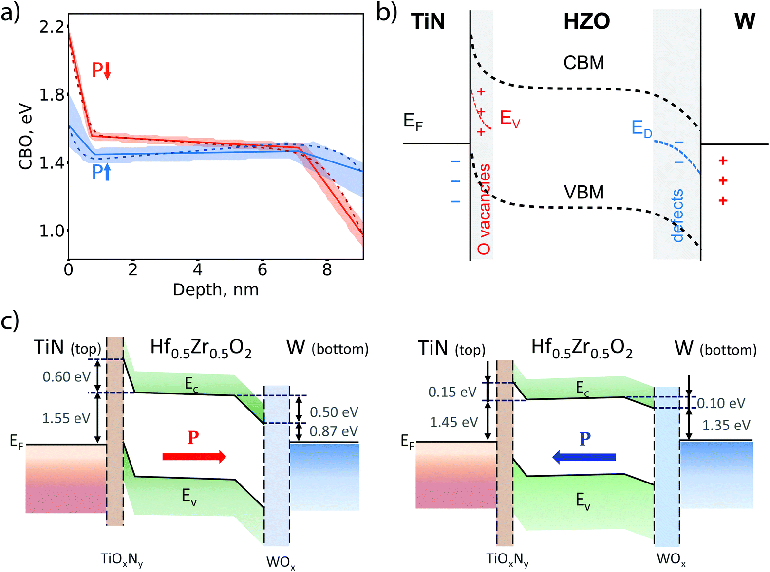 | ||
| Fig. 3 (a) The derived potential distribution (solid) with the confidence regions (semi-transparent) across FE-HZO layer for up (red) and down (blue) polarization orientations and the results of theoretical modelling (dashed line); (b) schematic representation of the model structure comprising positively charged oxygen vacancies and negatively charged structural defects in HZO layer at the top and bottom interfaces, respectively. Oxygen vacancy (EV) and defect (ED) energy levels are indicated by the red and blue dashed lines, respectively. The negative (positive) charges in the TiN (W) electrodes are due to the difference in the effective work functions of the electrodes (including oxidized interfaces) in contact with HZO, resulting in the built-in electric field across the HZO layer independent of polarization orientation. The conduction band minimum (CBM) and the valence band maximum (VBM) are schematically indicated by the dashed lines. (c) Full potential energy profile in TiN/HZO/W ferroelectric capacitor for two opposite polarization directions reconstructed from the experimental data. | ||
This plot takes into account the conduction band offsets at the TiN/HZO and HZO/W interfaces which are determined using the well-known method.31,32 According to this method, the conduction band offset (CBO) at a given interface is determined by:23,31
| CBO = Eg − ((BEHf 4f)int − (BEHf 4f − VBM)ref), |
The obtained potential profile across the ferroelectric HZO layer demonstrates that the depolarizing electric field is largely screened near the interfaces, and in the interior region of HZO, it nearly vanishes irrespective of polarization orientation. This observation indicates the presence of space charges in the interfacial regions of HZO, which effectively screen the depolarizing field. This behavior points to the presence of defects and other imperfections in the HZO layer accumulating the polarization-dependent space charge.
To elucidate possible correlations between the established electronic properties and structural distortions within the HZO layer, we have performed STEM analysis of the cycled TiN/HZO/W/Si samples used in HAXPES (Fig. 4). As is evident from Fig. 4a and b, there is an oxidized WOx layer at the HZO/W interface, and this interface appears to be rougher than the TiN/HZO interface. We note that the WOx layer is formed at the HZO/W interface upon exposure of the W film surface to atmospheric air prior to the HZO layer growth. The atomic resolution STEM analysis (Fig. 4c and d) reveals that the dominant structural phase of the grown HZO layer is the orthorhombic Pca21 phase, which is capable of supporting switchable ferroelectric polarization. The detailed description of the TEM based phase identification methodology can be found in ref. 15, 33 and 34. There are, however, grains of the non-ferroelectric monoclinic HZO phase at the bottom interface, which coexist with ferroelectric orthorhombic bulk grains within the film and can be distinguished based on the projected atom arrangement. Fig. 4c and d show that a monoclinic region is separated by an interphase boundary from an orthorhombic region, similar to those previously reported for polycrystalline hafnia and epitaxial zirconia ferroelectrics.34,35 HAADF STEM additionally reveals the presence of several unit cells of strained/distorted HZO regions at the interface with the W electrode, as seen from Fig. 4c and d. These regions may form during the growth of the HZO layer on the rough surface of oxidized W due to misfit strain. They may serve as sinks for non-ferroelectric space charges as they dynamically respond to polarization reversal by screening the depolarizing field at the HZO/W interface.
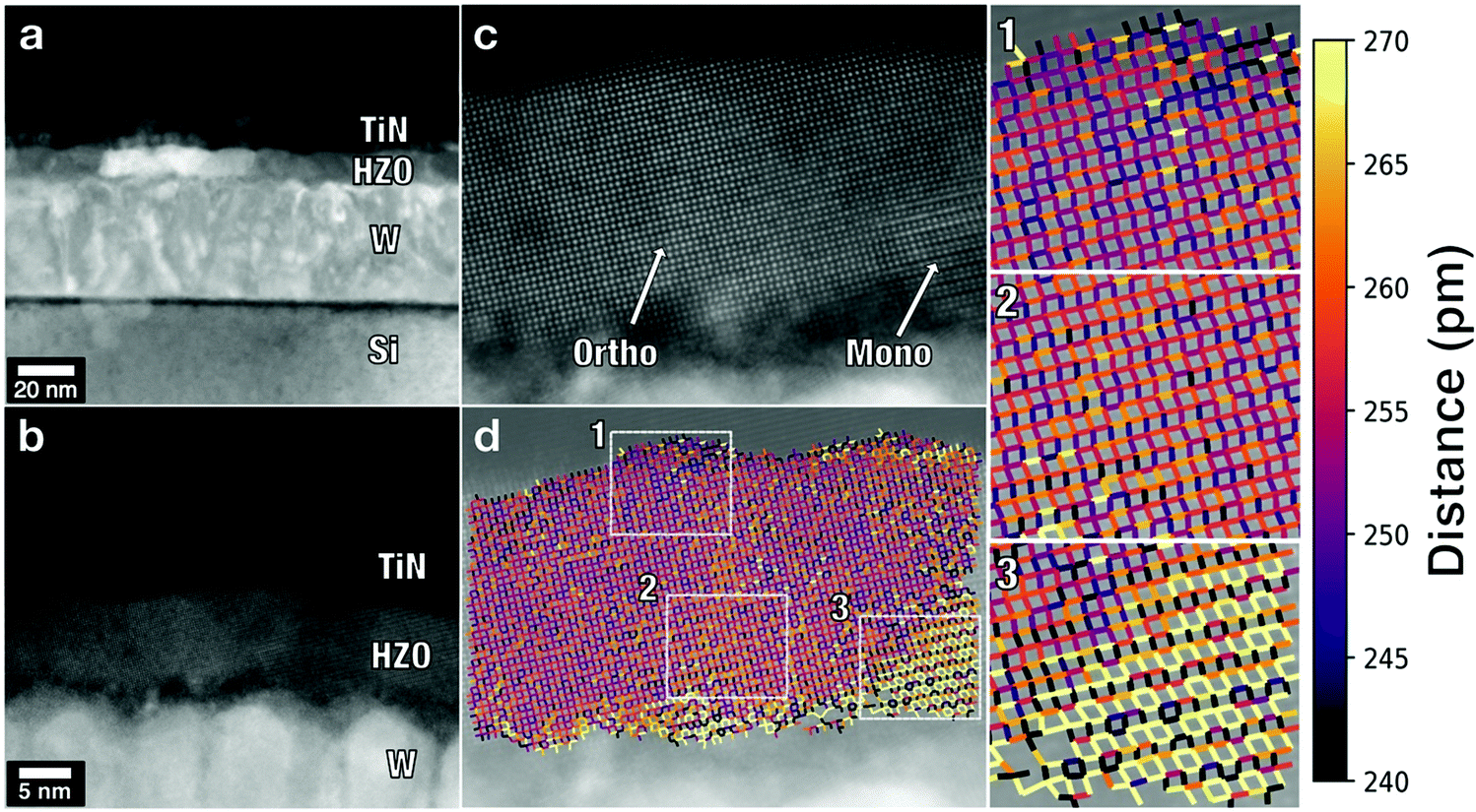 | ||
| Fig. 4 (a) and (b) HAADF-STEM images indicating film stacks and representative roughness. (c) and (d) HAADF STEM imaging with and without atom column distances measured across a representative HZO grain from the electrically-cycled sample with expanded insets showing (1) the orthorhombic grain interface with TiN, (2) the orthorhombic grain film bulk, and (3) the interface of the monoclinic grain with the W electrode. | ||
At the top TiN/HZO interface, the likely origin of the space charge in HZO is evident from our analysis of the Ti 2p core-level line acquired by HAXPES. We find that, in addition to the metallic component, the Ti 2p spectra contain features attributed to the oxidized TiN, i.e. TiOxNy, and such component is particularly present in contact with HZO (Fig. 2a and ESI section S6†). The oxidation of TiN at the interface with HZO has been observed previously,23 which is corroborated here by the observation of strain at the interface via HAADF STEM36 and by the occurrence of redox reactions during rapid thermal annealing at T = 400 °C. Such redox reactions imply the formation of oxygen vacancies in the HZO region adjacent to TiN (which eventually may give rise to the resistive switching effect in HZO). It is reasonable to assume that biasing of the device with voltage pulses U ∼ ±3 V during polarization switching results in charging/discharging of these oxygen vacancies in a ∼1 nm-thick HZO sublayer close to the TiN interface, thus yielding a non-linear shape of the potential distribution. Such interfacial layers with strain/distortion have been observed at TiN/hafnia interfaces previously,29,33,37 and also occur in our samples, as seen from Fig. 4c and d.
To support the proposed qualitative explanation of the polarization-dependent potential shape in terms of the charged oxygen vacancies and other structural defects, we develop a quantitative model with realistic parameters. The schematic representation of the model is shown in Fig. 3(b). Within this model, we assume that there are several sources of charges, which contribute to the resulting electrostatic potential energy profile. First, there are screening charges in the electrodes, positive in W (including the interfacial WOx layer) and negative in TiN (including the interfacial TiOxNy layer). These charges originate from the difference in their effective work functions and produce a polarization independent electric field pointing toward the TiN electrode. There are also polarization charges at both ferroelectric/electrode interfaces (not shown in Fig. 3(b)), which sign is reversed with ferroelectric polarization. As is evident from our experimental data (Fig. 3(a)), however, switching the polarization does not reverse the electrostatic potential energy (though affects its magnitude and profile), which remains higher at the top HZO layer. Therefore, independent of polarization orientation, there is an electric field in the HZO layer pointing toward the top TiN electrode.
This residual electric field is further screened by non-ferroelectric space charges in the ferroelectric originating from the positively charged oxygen vacancies and negatively charged structural defects at the top and bottom interfaces, respectively (Fig. 3(b)). More specifically, we assume that oxygen vacancies are formed within a thin layer of thickness lV close to the TiN/HZO interface and have single energy level EV and constant concentration NV. However, they can be neutral or charged according to the Fermi–Dirac statistics, depending on their energy level with respect to the Fermi level at the particular depth, as described in ESI section S6.† The electric potential built up by the charged oxygen vacancies in HZO layer depends on their initial concentration NV and their energy levels EV in the band gap, which are assumed to be independent of the charge state. Alternatively, the electric potential in a layer of thickness lD at the bottom HZO/W interface is shaped by chargeable defects generated due to structural imperfections with the total concentration ND and energy level ED in the band gap. The boundary conditions for two opposite ferroelectric polarization orientations are set by the electric potential values at the Ti/HZO and HZO/W interfaces determined from our experiment. As the result, the solution of the Poisson equation is unique and independent of the charges external to the HZO layer. By fitting the experimentally derived electric potential profile for both polarization orientations with this model, where lV, NV, lD, EV, ND, and ED are taken as fitting parameters, we find their values.
The detailed description of the calculation methodology is presented in ESI section S7.† The obtained fitting results, shown in Fig. 2e, yield oxygen vacancy concentration NV = 7.3 × 1020 cm−3 at the energy level EV ≈ 1.5 eV with respect to the conduction band edge in the ∼1 nm thick HZO layer adjacent to the top interface, which lies within the range of theoretically predicted values.38 The derived concentration of defects in the ∼3 nm-thick layer at the bottom interface is ND = 3 × 1020 cm−3 at the same energy ED ≈ 1.4 eV.
Charged oxygen vacancies in hafnia-zirconia films, particularly at the interface with an electrode, were previously identified as the cause for the observed instability of ferroelectric performance.39,40 The overall concentration of charged oxygen vacancies in the “bulk” of the HZO film ∼1 × 1020 cm−3 derived in that study is in surprisingly good agreement with the results from our modelling yielding VO+ concentration at the interfaces NV+ ≈ 3–7 × 1020 cm−3, depending on the polarization orientation.
Finally, since we use HAXPES technique to probe properties of the ferroelectric capacitors, it is worth to discuss possible detrimental effects of intense synchrotron X-ray radiation on the device structure as well as the electronic and electrical properties. Indeed, there have been several reports on the damage from the X-ray beam in oxides [see ref. 41 and reference therein], which may lead to changes in stoichiometry and phase composition. However, careful analysis of leakage currents and remnant polarization values in the devices under investigation acquired in situ during HAXPES experiment does not show noticeable changes of electrical properties following X-ray illumination (ESI Fig. S3 and S4†). We take this fact as an evidence of no (or negligible) effect of X-ray beam on the generation of (electrically active) defects.
In addition, we note that a ferroelectric capacitor in a FRAM memory array might be used on a different time scale compared to the HAXPES measurements. The readout operation in memory devices after a polarization reversal might be covering a time scale from nanoseconds to years. On the other hand, due to charge trapping/detrapping in the interfacial layers, the local electrostatic potential distribution across nanoscale ferroelectric layer may change on the time scale of up to tens of hours.42 HAXPES measurements in this work were taken after ∼10 min upon polarization switching at the “equilibrium” conditions judging from the electrical characteristics of the device under investigation.
4. Conclusions
In conclusion, we have developed new methodology to derive local electrostatic potential distribution across nanoscale dielectric layers based on the standing-wave hard X-ray photoelectron spectroscopy and used it to elucidate electric potential distribution in functional ferroelectric TiN/Hf0.5Zr0.5O2/W capacitor devices. The performed operando measurements revealed a non-linear potential profile across the ferroelectric Hf0.5Zr0.5O2 layer, implying the presence of non-ferroelectric space charges close to the interfaces, which effectively screen the depolarizing electric field. The depth-selective chemical analysis of the TiN electrode pointed at the redox reaction at the top TiN/Hf0.5Zr0.5O2 interface yielding the formation of oxygen vacancies in the ferroelectric layer. The atomic-scale STEM analysis indicated the structural relaxation and local phase transition at the bottom Hf0.5Zr0.5O2/W interface presumably accompanied by the formation of defects with energy levels in the band gap. Verified by our theoretical modelling, the proposed model explained the observed shape and changes of the electric potential in terms of polarization and depth dependent distribution of charged defects across the ferroelectric Hf0.5Zr0.5O2 layer. The experimental methodology presented here may be used to characterize the electric potential distribution at the nanoscale in real devices. The obtained quantitative results are important for the understanding of the functional properties of ferroelectric HfO2 based capacitors and may be useful for the implementation of novel non-volatile memory devices.Conflicts of interest
There are no conflicts to declare.Acknowledgements
This work was performed using equipment of MIPT Center of Shared Facilities and with financial support by the Russian Science Foundation (Grant No. 18-12-00434). We acknowledge DESY (Hamburg, Germany), a member of the Helmholtz Association HGF, for the provision of experimental facilities of beamline P09. Funding for the HAXPES instrument at beamline P09 by the Federal Ministry of Education and Research (BMBF) under contracts 05KS7UM1 and 05K10UMA with Universität Mainz; 05KS7WW3, 05K10WW1 and 05K13WW1 with Universität Würzburg is gratefully acknowledged. EDG acknowledges support for this work through a National Science Foundation Graduate Research Fellowship (DGE-1252376). AK, EDG, and JML acknowledge support from the National Science Foundation (DMR-1350273) and performed their work in part at the Analytical Instrumentation Facility (AIF) at North Carolina State University, which is supported by the State of North Carolina and the National Science Foundation (award number ECCS-1542015). The AIF is a member of the North Carolina Research Triangle Nanotechnology Network (RTNN), a site in the National Nanotechnology Coordinated Infrastructure (NNCI).References
- S. Mathews, R. Ramesh, T. Venkatesan and J. Benedetto, Ferroelectric field effect transistor based on epitaxial perovskite heterostructures, Science, 1997, 276, 238–240 CrossRef CAS PubMed.
- M. Okuyama, Features, Principles and Development of Ferroelectric–Gate Field-Effect Transistors, in Ferroelectric-Gate Field Effect Transistor Memories. Topics in Applied Physics vol. 131, ed. B. Park, H. Ishiwara, M. Okuyama, S. Sakai and S. Yoon, Springer Netherlands, 2016, pp. 3–20 Search PubMed.
- M. Y. Zhuravlev, R. F. Sabirianov, S. S. Jaswal and E. Y. Tsymbal, Giant electroresistance in ferroelectric tunnel junctions, Phys. Rev. Lett., 2005, 94, 246802 CrossRef.
- V. Garcia and M. Bibes, Ferroelectric tunnel junctions for information storage and processing, Nat. Commun., 2014, 5, 4289 CrossRef CAS PubMed.
- J. P. Velev, J. D. Burton, M. Y. Zhuravlev and E. Y. Tsymbal, Predictive modelling of ferroelectric tunnel junctions, npj Comput. Mater., 2016, 2, 16009 CrossRef.
- K. Sugibuchi, Y. Kurogi and N. Endo, Ferroelectric field-effect memory device using Bi4Ti3O12 film, J. Appl. Phys., 1975, 2877, 46 Search PubMed.
- E. Yurchuk, J. Müller, R. Hoffmann, J. Paul, D. Martin, R. Boschke, T. Schlösser, S. Müller, S. Slesazeck, R. Bentum, M. Trentzsch, U. Schröder and T. Mikolajick, HfO2-Based Ferroelectric Field-Effect Transistors with 260 nm Channel Length and Long Data Retention, 4th IEEE International Memory Workshop, 2012, p. 1–4 Search PubMed.
- S. Mueller, J. Müller, R. Hoffmann, E. Yurchuk, T. Schlösser, R. Boschke, J. Paul, M. Goldbach, T. Herrmann, A. Zaka, U. Schröder and T. Mikolajick, From MFM Capacitors Toward Ferroelectric Transistors: Endurance and Disturb Characteristics of HfO2-Based FeFET Devices, IEEE Trans. Electron Devices, 2013, 60, 4199–4205 CAS.
- V. Garcia, S. Fusil, K. Bouzehouane, S. Enouz-Vedrenne, N. D. Mathur, A. Barthelemy and M. Bibes, Giant Tunnel Electroresistance for Non-destructive Readout of Ferroelectric States, Nature, 2009, 460, 81–84 CrossRef CAS PubMed.
- A. Gruverman, D. Wu, H. Lu, Y. Wang, H. W. Jang, C. M. Folkman, M. Y. Zhuravlev, D. Felker, M. Rzchowski, C.-B. Eom and E. Y. Tsymbal, Tunneling Electroresistance Effect in Ferroelectric Tunnel Junctions at the Nanoscale, Nano Lett., 2009, 9, 3539–3543 CrossRef CAS PubMed.
- A. Crassous, V. Garcia, K. Bouzehouane, S. Fusil, A. H. G. Vlooswijk, G. Rispens, B. Noheda, M. Bibes and A. Barthélémy, Giant Tunnel Electroresistance with PbTiO3 Ferroelectric Tunnel Barriers, Appl. Phys. Lett., 2010, 96, 042901 CrossRef.
- H. Yamada, V. Garcia, S. Fusil, S. Boyn, M. Marinova, A. Gloter, S. Xavier, J. Grollier, E. Jacquet, C. Carretero, C. Deranlot, M. Bibes and A. Barthelemy, Giant Electroresistance of Super-Tetragonal BiFeO3-Based Ferroelectric Tunnel Junctions, ACS Nano, 2013, 7, 5385–5390 CrossRef CAS PubMed.
- A. Zenkevich, M. Minnekaev, Y. Matveyev, Y. Lebedinskii, K. Bulakh, A. Chouprik, A. Baturin, K. Maksimova, S. Thiess and W. Drube, Electronic band alignment and electron transport in Cr/BaTiO3/Pt ferroelectric tunnel junctions, Appl. Phys. Lett., 2013, 102, 06290 CrossRef.
- T. S. Boescke, J. Mueller, D. Braeuhaus, U. Schroeder and U. Boettger, Ferroelectricity in hafnium oxide thin films, Appl. Phys. Lett., 2011, 99, 102903 CrossRef.
- X. Sang, E. D. Grimley, T. Schenk, U. Schroeder and J. M. LeBeau, On the Structural Origins of Ferroelectricity in HfO2 Thin Films, Appl. Phys. Lett., 2015, 106, 162905 CrossRef.
- S. Clima, D. J. Wouters, C. Adelmann, T. Schenk, U. Schroder, M. Jurczak and G. Pourtois, Identification of the Ferroelectric Switching Process and Dopant-Dependent Switching Properties in Orthorhombic HfO2: A first principles insight, Appl. Phys. Lett., 2014, 104, 092906 CrossRef.
- D. Zhou, J. Muller, J. Xu, S. Knebel, D. Brauhaus and U. Schroder, Insights into Electrical Characteristics of Silicon Doped Hafnium Oxide Ferroelectric Thin Films, Appl. Phys. Lett., 2012, 100, 082905 CrossRef.
- S. Zarubin, E. Suvorova, M. Spiridonov, D. Negrov, A. Chernikova, A. Markeev and A. Zenkevich, Fully ALD-grown TiN/Hf0.5Zr0.5O2/TiN stacks: Ferroelectric and structural properties, Appl. Phys. Lett., 2016, 109, 192903 CrossRef.
- M. Seo, M.-H. Kang, S.-B. Jeon, H. Bae, J. Hur, B. C. Jang, S. Yun, S. Cho, W.-K. Kim, M.-S. Kim, K.-M. Hwang, S. Hong, S.-Y. Choi and Y.-K. Choi, First Demonstration of a Logic-Process Compatible Junctionless Ferroelectric FinFET Synapse for Neuromorphic Applications, IEEE Electron Device Lett., 2018, 39, 1445–1448 CAS.
- F. Ambriz-Vargas, G. Kolhatkar, M. Broyer, A. Hadj-Youssef, R. Nouar, A. Sarkissian, R. Thomas, C. Gomez-Yáñez, M. A. Gauthier and A. Ruediger, A Complementary Metal Oxide Semiconductor Process-Compatible Ferroelectric Tunnel Junction, ACS Appl. Mater. Interfaces, 2017, 9, 13262–13268 CrossRef CAS PubMed.
- F. Chen and A. Klein, Polarization dependence of Schottky barrier heights at interfaces of ferroelectrics determined by photoelectron spectroscopy, Phys. Rev. B: Condens. Matter Mater. Phys., 2012, 86, 094105 CrossRef.
- E. Kröger, A. Petraru, A. Quer, R. Soni, M. Kalläne, N. Pertsev, H. Kohlstedt and K. Rossnagel, In situ hard X-ray photoemission spectroscopy of barrier-height control at metal/PMN-PT interfaces, Phys. Rev. B: Condens. Matter Mater. Phys., 2016, 93, 235415 CrossRef.
- Y. Matveyev, D. Negrov, A. Chernikova, Y. Lebedinskii, R. Kirtaev, S. Zarubin, E. Suvorova, A. Gloskovskii and A. Zenkevich, Effect of Polarization Reversal in Ferroelectric TiN/Hf0.5Zr0.5O2/TiN Devices on Electronic Conditions at Interfaces Studied in Operando by Hard X-ray Photoemission Spectroscopy, ACS Appl. Mater. Interfaces, 2017, 9, 43370–43376 CrossRef CAS PubMed.
- C. S. Fadley, Hard X-ray photoemission with angular resolution and standing-wave excitation, J. Electron Spectrosc. Relat. Phenom., 2013, 190B, 165–179 CrossRef.
- S.-C. Lin, C.-T. Kuo, R. B. Comes, J. E. Rault, J.-P. Rueff, S. Nemšák, A. Taleb, J. B. Kortright, J. Meyer-Ilse, E. Gullikson, P. V. Sushko, S. R. Spurgeon, M. Gehlmann, M. E. Bowden, L. Plucinski, S. A. Chambers and C. S. Fadley, Interface properties and built-in potential profile of a LaCrO3/SrTiO3 superlattice determined by standing-wave excited photoemission spectroscopy, Phys. Rev. B: Condens. Matter Mater. Phys., 2018, 98, 165124 CrossRef CAS.
- M. Marinova, J. E. Rault, A. Gloter, S. Nemsak, G. K. Palsson, J.-P. Rueff, C. S. Fadley, C. Carrétéro, H. Yamada, K. March, V. Garcia, S. Fusil, A. Barthélémy, O. Stéphan, C. Colliex and M. Bibes, Depth Profiling Charge Accumulation from a Ferroelectric into a Doped Mott Insulator, Nano Lett., 2015, 15, 2533–2541 CrossRef CAS.
- A. Chernikova, M. Kozodaev, A. Markeev, D. Negrov, M. Spiridonov, S. Zarubin, O. Bak, P. Buragohain, H. Lu, E. Suvorova, A. Gruverman and A. Zenkevich, Ultrathin Hf0.5Zr0.5O2 Ferroelectric Films on Si, ACS Appl. Mater. Interfaces, 2016, 8, 7232–7237 CrossRef CAS PubMed.
- A. Gloskovskii, G. Stryganyuk, G. Fecher, C. Felser, S. Thiess, H. Schulz-Ritter, W. Drube, G. Berner, M. Sing, R. Claessen and M. Yamamoto, Magnetometry of buried layers—Linear magnetic dichroism and spin detection in angular resolved hard X-ray photoelectron spectroscopy, J. Electron Spectrosc. Relat. Phenom., 2012, 185, 47–52 CrossRef CAS.
- C. Richter, T. Schenk, M. H. Park, F. A. Tscharntke, E. D. Grimley, J. M. LeBeau, C. Zhou, C. M. Fancher, J. L. Jones, T. Mikolajick and U. Schroeder, Si Doped Hafnium Oxide—A “Fragile” Ferroelectric System, Adv. Electron. Mater., 2017, 3, 1700131 CrossRef.
- J. F. Scott, L. Kammerdiner, M. Parris, S. Traynor, V. Ottenbacher, A. Shawabkeh and W. F. Oliver, Switching Kinetics of Lead Zirconate Titanate Submicron Thin-Film Memories, J. Appl. Phys., 1988, 64, 787–792 CrossRef CAS.
- E. Kraut, R. Grant, J. Waldrop and S. Kowalczyk, Semiconductor core-level to valence-band maximum binding-energy differences: Precise determination by X-ray photoelectron spectroscopy, Phys. Rev. B: Condens. Matter Mater. Phys., 1983, 28, 1965–1977 CrossRef CAS.
- Y. Lebedinskii, A. Zenkevich and E. Gusev, Measurements of metal gate effective work function by x-ray photoelectron spectroscopy, J. Appl. Phys., 2007, 101, 074504 CrossRef.
- E. D. Grimley, T. Schenk, X. Sang, M. Pešić, U. Schroeder, T. Mikolajick and J. M. LeBeau, Structural Changes Underlying Field-Cycling Phenomena in Ferroelectric HfO2 Thin Films, Adv. Electron. Mater., 2016, 2, 1600173 CrossRef.
- E. D. Grimley, T. Schenk, T. Mikolajick, U. Schroeder and J. M. LeBeau, Atomic Structure of Domain and Interphase Boundaries in Ferroelectric HfO2, Adv. Mater. Interfaces, 2018, 5, 1701258 CrossRef.
- S. Choi, T. Shiraishi, T. Kiguchi, T. Shimizu, H. Funakubo and T. J. Konno, Formation of polar phase in Fe-doped ZrO2 epitaxial thin films, Appl. Phys. Lett., 2018, 113, 262903 CrossRef.
- M. Pešić, F. P. G. Fengler, L. Larcher, A. Padovani, T. Schenk, E. D. Grimley, X. Sang, J. M. LeBeau, S. Slesazeck, U. Schroeder and T. Mikolajick, Physical Mechanisms behind the Field-Cycling Behavior of HfO2-Based Ferroelectric Capacitors, Adv. Funct. Mater., 2016, 26, 4601–4612 CrossRef.
- U. Schroeder, C. Richter, M. H. Park, T. Schenk, M. Pešić, M. Hoffmann, F. P. G. Fengler, D. Pohl, B. Rellinghaus, C. Zhou, C.-C. Chung, J. L. Jones and T. Mikolajick, Lanthanum-Doped Hafnium Oxide: A Robust Ferroelectric Material, Inorg. Chem., 2018, 57, 2752–2765 CrossRef CAS PubMed.
- J. Gavartin, D. M. Ramo, A. Shluger, G. Bersuker and B. Lee, Negative oxygen vacancies in HfO2 as charge traps in high-k stacks, Appl. Phys. Lett., 2016, 89, 082908 CrossRef.
- F. P. G. Fengler, R. Nigon, P. Muralt, E. D. Grimley, X. Sang, V. Sessi, R. Hentschel, J. M. LeBeau, T. Mikolajick and U. Schroeder, Analysis of Performance Instabilities of Hafnia-Based Ferroelectrics Using Modulus Spectroscopy and Thermally Stimulated Depolarization Currents, Adv. Electron. Mater., 2018, 4, 1700547 CrossRef.
- A. Chouprik, M. Spiridonov, S. Zarubin, R. Kirtaev, V. Mikheev, Y. Lebedinskii, S. Zakharchenko and D. Negrov, Wake-Up in a Hf0.5Zr0.5O2 Film: A Cycle-by-Cycle Emergence of the Remnant Polarization via the Domain Depinning and the Vanishing of the Anomalous Polarization Switching, ACS Appl. Electron. Mater., 2019, 1(3), 275 CrossRef CAS.
- S. H. Chang, J. Kim, C. Phatak, K. D'Aquila, S. K. Kim, J. Kim, S. J. Song, C. S. Hwang, J. A. Eastman, J. W. Freeland and S. Hong, X-ray Irradiation Induced Reversible Resistance Change in Pt/TiO2/Pt Cells, ACS Nano, 2014, 8, 1584–1589 CrossRef CAS PubMed.
- P. Buragohain, A. Erickson, P. Kariuki, T. Mittmann, C. Richter, P. D. Lomenzo, H. Lu, T. Schenk, T. Mikolajick, U. Schroeder and A. Gruverman, Fluid Imprint and Inertial Switching in Ferroelectric La:HfO2 Capacitors, ACS Appl. Mater. Interfaces, 2019, 11, 35115–35121 CrossRef CAS PubMed.
Footnote |
| † Electronic supplementary information (ESI) available. See DOI: 10.1039/c9nr05904k |
| This journal is © The Royal Society of Chemistry 2019 |