
 Open Access Article
 This Open Access Article is licensed under a Creative Commons Attribution-Non Commercial 3.0 Unported Licence
Directed nanoscale metal deposition by the local perturbation of charge screening at the solid–liquid interface†
Mark
Aarts
and
Esther
Alarcon-Llado
 *
*
Center for Nanophotonics, NWO-I Amolf, Science Park 104, 1098 XG Amsterdam, Netherlands. E-mail: e.alarconllado@amolf.nl
First published on 4th October 2019
Abstract
Understanding and directing electrochemical reactions below the micrometer scale is a long-standing challenge in electrochemistry. Confining reactions to nanoscale areas paradoxically requires both isolation from and communication with the bulk electrolyte in terms of electrochemical potential and access of ions, respectively. Here, we demonstrate the directed electrochemical deposition of copper nanostructures by using an oscillating nanoelectrode operated with an atomic force microscope (AFM). Strikingly, the writing is only possible in highly dilute electrolytes and for a particular combination of AFM and electrochemical parameters. We propose a mechanism based on cyclic charging and discharging of the electrical double layer (EDL). The extended screening length and slower charge dynamics in dilute electrolytes allow the nanoelectrode to operate inside, and disturb, the EDL even for large oscillation amplitudes (∼100 nm). Our unique approach can not only be used for controlled additive nano-fabrication but also provides insights into ion behavior and EDL dynamics at the solid–liquid interface.
Introduction
Electrochemical deposition can revolutionize the fabrication of (opto)electronic nanodevices if carefully controlled at the nanoscale. Among its advantages are the relatively small infrastructure costs, low thermal budget and fine dynamic control over reaction kinetics and thermodynamics, which does not exist with any other synthetic method. However, the biggest challenge in integrating electrodeposition and nanotechnology is the controlled down-scaling of chemical reactions down to the nanoscale.1,2 This control would provide additional freedom in designing free-form nano-architectures with extraordinary properties and functionalities.3–7One approach to confine growth is by spatially restricting the electrochemical cell or the feeding of precursors, such as in meniscus confined electrodeposition, local dispensing of ions, or electrohydrodynamic jet printing.8–13 A different strategy is the direct electrochemical writing with small electrodes. Complex 3D structures have been successfully made at the scale of tens to few hundredths of microns by using scanning microelectrodes, where the size of the electrode and its distance to the sample define the fabrication resolution.14,46
At the nanoscale, scanning probe microscopes (SPM) have demonstrated high precision in nanostructuring metal, semiconductor and oxide surfaces under gas or liquid conditions, based on a variety of tip–surface interactions.15–18 However, in most cases, growth is restricted to a few nanometers in height (such as clusters). Additive electrochemical nano-fabrication of structures beyond atomic cluster size with scanning probes has been difficult, contrary to what could be expected from conventional electrochemistry. This is due to the fact that when the tip/substrate gap is of the order of nanometers, the reaction dynamics are governed by a complex interplay of electrochemical potential distributions,19 poor communication with the bulk solution, and mass transport limitations preventing ion access into the small gap.20–22 In general, effects of the structure and dynamics of the electrical double layer (EDL) at the solid–liquid interface on nanoscale electrochemistry are not fully understood.23,24 In the past years, several groups have focused on using SPM techniques to probe the solid–liquid interface,25–32 in terms of specific adsorption,33 charge density, and screening.34,35 In all these studies, care was taken to ensure minimal perturbation of the EDL by the probing tip. However, it has been suggested that in some cases, the probe may strongly perturb the charge distribution at the interface.20,36
Schuster and co-workers demonstrated the etching and deposition of metals with micrometer resolution by locally polarizing the EDL at the water–substrate interface upon the application of a voltage pulse at a micro-electrode.37 The authors described the reaction confinement by considering a simple RC equivalent circuit, concluding that nanometer resolution would require fs pulses. However, this timescale is much faster than the typical electric double layer dynamics (∼ns–μs).38 Interestingly, nanoscale local etching and deposition has been demonstrated with μs pulses to a scanning tunneling microscope (STM) tip.39–41
In this work, we take advantage of the capabilities of an electrochemical atomic force microscope (EC-AFM) tip to dynamically perturb the EDL in order to control growth at the nanoscale. We achieve this by using a highly dilute electrolyte and a highly asymmetric tip–substrate system (in terms of material and potential). We demonstrate direct electro-deposition of copper on gold, with lateral dimensions down to 50 nanometers and an aspect ratio slightly above 0.5 for a writing speed of 3 nm s−1. We show a critical dependence of the ability to confine growth on the salt concentration, and the dynamics of the tip movement during the writing. We propose a local growth mechanism facilitated by a combination of periodic disruption and build-up of the EDL, followed by forced electrodeposition due to the strong perturbation of the electrochemical potential between the tip and the sample.
The ability to control solution-based growth down to the nanoscale can revolutionize nanofabrication, by enabling the manufacturing of combined logical circuits, LEDs, photodetectors and many other (opto)electronic devices on the same platform with nanoscale resolution. Additionally, local deposition with dynamic EC-AFM can be used as an indirect means to probe EDL dynamics in general, which has a strong impact in any electrochemical process such as in batteries, or elecrocatalysis.
Results
Direct writing of copper nanostructures
We control the local growth of copper on gold by applying a potential difference directly between a Au substrate and an AFM tip in a dilute aqueous electrolyte (1 μM CuSO4). The tip apex, which is made of Pt, is the only part of the cantilever that is exposed to the liquid.42 During writing, the AFM is operated in the PeakForce (PF) tapping mode, where the cantilever is driven by a sinusoidal signal far below its resonance frequency (2 kHz in this work) (Fig. 1a, and methods). In this mode, the force exerted by the tip on the sample is used as the feedback signal (3 to 30 nN in this work), while the intermittent contact results in minimal lateral forces on the substrate. By moving the tip along a programmed xy trajectory, arbitrary shapes can be written (Fig. 1b and c).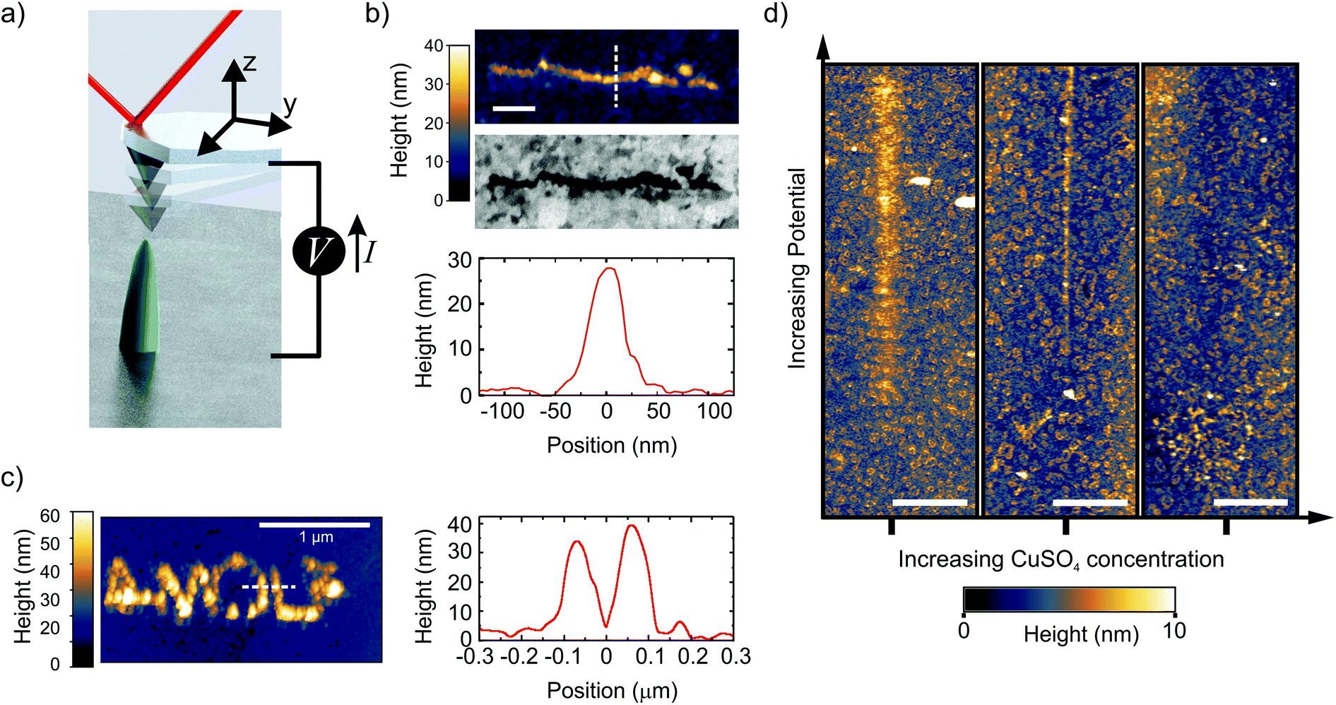 | ||
| Fig. 1 Direct writing of copper with dynamic EC-AFM. (a) Cartoon representing the EC-AFM writing set-up. (b) Ex situ AFM-topography, cross-section height profile, and in-column SEM, of a 1 μm long line deposited in a single EC-AFM pass at 3 nm s−1 with an applied potential of 1.7 V. (c) Ex situ AFM-topography and cross-section height profile of the written AMOLF logo, deposited in a consecutive double pass at 30 nm s−1 and 3 nm s−1 with an applied potential of 1.7 V. The writing in (b) and (c) were done in 1 μM CuSO4 solutions. Scale bar is 200 nm in Fig. 1b. (d) In situ AFM topography, after following a 12 μm-long path across the center of each image while ramping the potential from 1 to 2.5 V (in the first two panels) and 1.2 to 2.7 V (in the rightmost panel). Three different concentrations of CuSO4 were used (from left to right: 1, 4 and 12 μM). The deposition disappears by increasing the concentration. The scale bar is 2 μm. | ||
Single lines down to a full width half maximum (FWHM) of ∼50 nm and as closely spaced as 125 nm are obtained with aspect ratios above 0.5 (line profiles in Fig. 1b and c). It should be noted that the extent of the deposition profile is in the order of the expected tip diameter, which is typically regarded as the lower limit on resolution in most SPM-based nanofabrication.18,43 The clear Z-contrast of the deposited structure with the gold substrate as obtained from backscattered electrons in a scanning electron microscope (SEM) highlights the chemical nature of the deposited copper wire, as is also found by energy dispersive X-ray (EDX) analysis from a larger structure (ESI-1†).
To enable the local writing, however, we find two counter-intuitive results that disagree with previously reported micro- and nano-SPM based electrochemical deposition mechanisms. First, we find that the local deposition only occurs when reducing the salt concentration down to a few μM. The panels in Fig. 1d show the topography after the tip is translated over a 12 μm long path with the PF feedback enabled and ramping the voltage (1 < V < 2.7 V) along the path. The figure clearly shows the deposition emerging with increasing potential in the case with the lowest ion concentration, which gradually disappears with increasing concentration. In fact, at concentrations above 10 μM, we are unable to observe any growth within our typical AFM scan range (∼15 μm) and parameters (ESI-2†). While increasing the concentration of CuSO4 should accelerate growth, mainly through facilitating mass transport, it is not in line with our observations. This is therefore a critical result and rules out other known writing mechanisms, such as AFM-induced local de-passivation of a metal substrate15,16 or electric-field enhanced mass transport.44–46 Second, no deposition is observed when the tip is kept at a fixed tip–substrate distance (ranging from 3 to 300 nm). In fact, we will illustrate that the AFM tip dynamics play a critical role in the direct writing mechanism.
Influence of electrochemical parameters
First, we investigate the electrochemical nature of the deposition process. The electrochemical behavior of the tip–substrate system is shown in Fig. 2a, where no current flows until a minimum potential of around 1.2 V is reached, after which the current increases exponentially. This is consistent with a minimum thermodynamic potential difference between the oxidation of water at the tip and copper reduction at the substrate.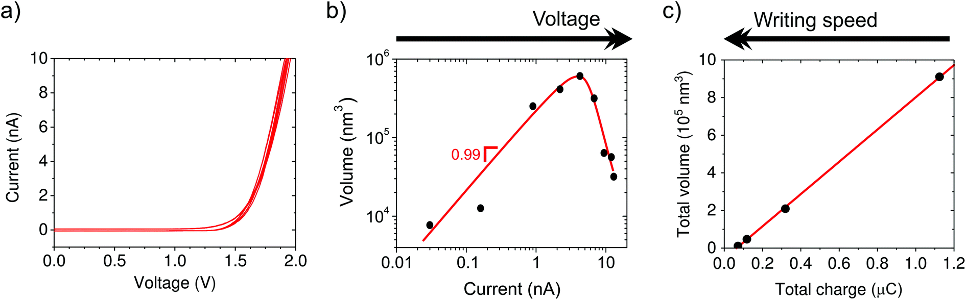 | ||
| Fig. 2 Electrochemical nature of the local Cu deposition. (a) Current–voltage characteristics of the tip-Au substrate two electrode system. At positive bias, current in the electrolyte flows from the tip to the substrate. (b) Linear scaling of the volume as a function of current in 1000 nm-long lines for a fixed set of AFM parameters. Different currents are obtained by increasing the applied potential. At high potentials/currents the deposition efficiency drops, most likely due to the competing hydrogen evolution reaction. The volume is obtained from ex situ AFM topography. (c) Volume of 1000 nm-long lines as a function of the total charge transferred for a given voltage and the same PeakForce parameters as in (b). The different points are obtained by different writing speeds, from 3 to 100 nm s−1. | ||
From ex situ AFM topography, we determine the deposited volume as a function of the total charge passed through the system, which is controlled by varying either the voltage (1.3 to 2.1 V in steps of 0.1 V, Fig. 2b) or writing time by means of the translation speed (3, 10, 30, and 100 nm s−1, Fig. 2c). The linear dependence of the volume on current supports the electrochemical nature of the process. However, the amount of charge required to obtain an equivalent volume of solid copper from Cu2+ is five orders of magnitude smaller than that derived from the measured current. This suggests that large stray currents are present across the substrate that do not result in copper growth, which is not surprising given the large surface area of our substrate electrode (∼5 cm2). Moreover, Fig. 2b shows that the deposition is suppressed at high currents/potentials most likely due to the competing proton reduction reaction, which leads to a “working” potential window. Actually, the formation of bubbles is observed underneath the tip at higher current densities (typically ∼20 nA).
The additive nature of the fabrication is highlighted by the increase in volume with time when driving the system at a fixed potential. In particular, the volume increases linearly with charge, but only after a certain threshold (Fig. 2c, black curve). We attribute the presence of a minimum amount of charge required for growth to kinetic limitations of the nucleation.
Influence of tapping dynamics
In the following, we investigate the impact of AFM tapping parameters on local growth to better understand the mechanism of confined electrochemistry. We adjust the tip position dynamics through the PeakForce amplitude (PFA) and the force setpoint (FS) parameters (Fig. 3a). The time-averaged tip–sample distance or gap size (<z>) and time in contact (CT) are estimated from the PFA and FS settings as described in the ESI-3.† The effect of the FS on <z> is quite significant. For instance, at the nominal spring constant of 1.5 N m−1 of our tips, the maximum gap size is reduced by 20 nm when the FS is increased by 30 nN, a value that may represent a large fraction of the oscillation amplitude (see ESI-3†).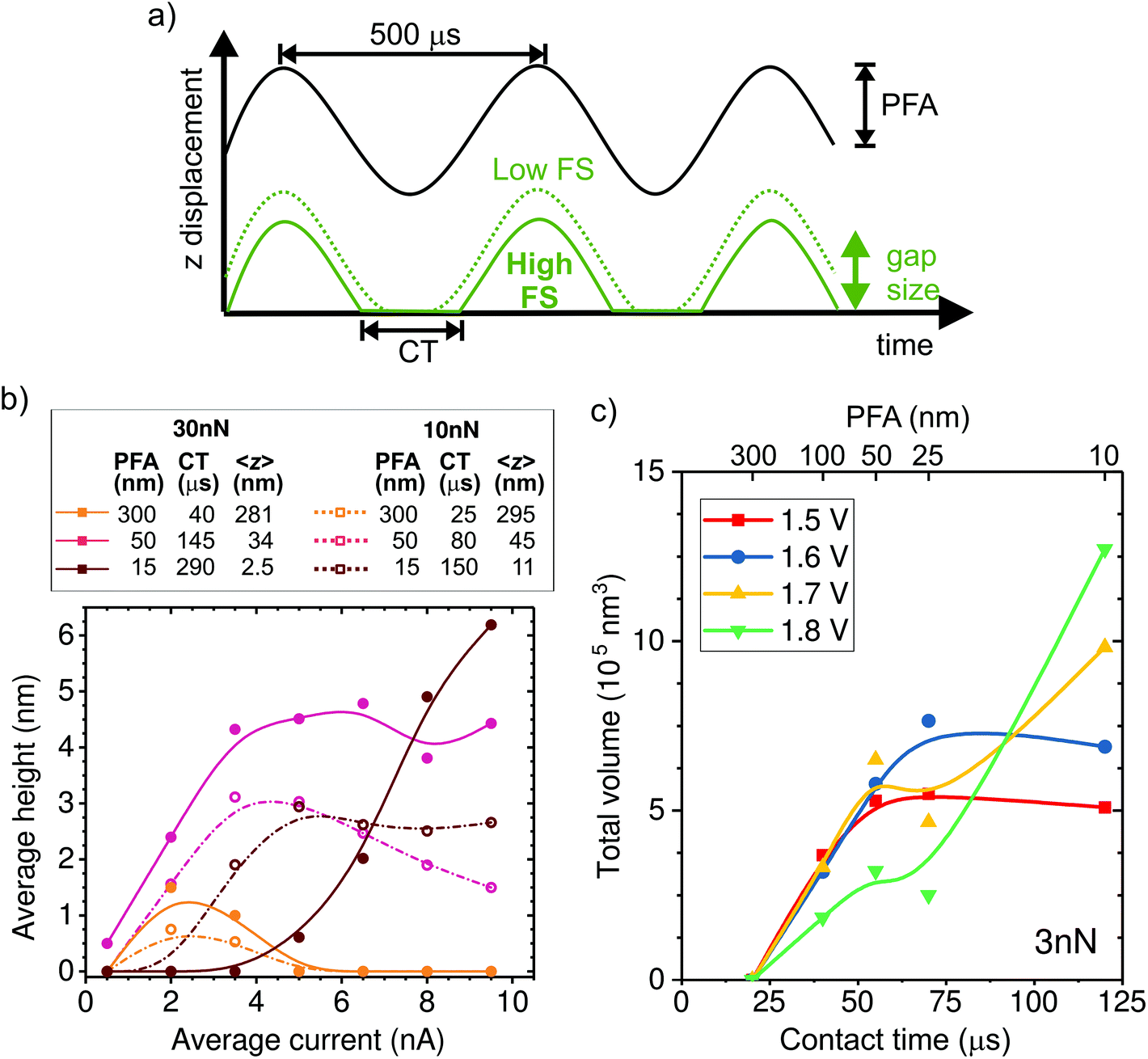 | ||
| Fig. 3 Influence of the AFM tip dynamics on the local deposition. (a) Representation of the tip dynamics over a few tapping cycles. The PeakForce oscillation amplitude (PFA) sets the amplitude of the drive signal (black curve). While the cantilever follows the drive signal, the actual tip position (green curves) and contact time (CT) depend on the force set point (FS) as well. As a result, the center of oscillation moves up and down as a function of both parameters. (b) Height of Cu lines, averaged along a 1000 nm path written at 10 nm s−1, as a function of applied current for different PFA and FS. The estimated CT and average gap size (<z>) during the oscillation are listed above. Both the height of the deposit and the optimal current change as a function of the oscillation parameters. (c) Total deposited volume in Cu lines written along a 500 nm path as a function of CT, which is controlled by changing the PFA from 10 to 300 nm. All lines are written with the same FS of 3 nN, a translation speed of 10 nm s−1 and at fixed bias voltages from 1.5 to 1.8 V (average currents of ∼1, 2.5, 4, 6.5 ± 0.5 nA). The figure displays a threshold contact time for deposition of ∼25 μs. | ||
The influence of the tip dynamics on the local growth is represented by the average maximum height of a line deposited along a 1000 nm-long path as a function of current (Fig. 3b). We do not observe a consistent trend in the width of the deposit as a function of the oscillation parameters or the current (ESI-4†). Here, the paths are followed at either 10 or 30 nN, corresponding to dashed and thick lines, respectively, and with three different oscillation amplitudes (15, 50 and 300 nm). The corresponding average gap size and contact time are listed in the table of Fig. 3b. Similar to Fig. 2b, local growth is favoured within a limited electrochemical window, leading to an optimal drive condition. Surprisingly, the optimal drive strongly depends on the AFM operation parameters. At large oscillation amplitudes, where the tip is above the substrate most of the time, little deposition is seen regardless of the force set point. This reinforces the notion that the process is not primarily driven by surface de-passivation from simple mechanical tip–sample interaction. We find that the share of time spent in contact with the sample appears to be a key parameter for determining the optimal driving condition for local growth. This is particularly evident at 15 nm amplitude, where height–current behavior for the two forces is quite different. Rather, the data for 10 nN resemble that of 30 nN with a similar contact time (i.e. amplitude of 50 nm).
In order to further investigate the link between CT and local deposition, we plot the total deposited volume as a function of CT (varied by means of the amplitude) for lines written at a fixed force of 3 nN and various potentials (Fig. 3c). The most striking feature in Fig. 3c is that growth is absent for all potentials when the contact time is shorter than ∼25 μs. The presence of a threshold value for the contact time is in line with the observation that no deposition is obtained with the tip held at a fixed distance above the surface (limit of zero contact). For times longer than the threshold, the deposited volume generally increases with CT. Interestingly, when writing at low drives (1.5 and 1.6 V), the volume saturates after ∼50 μs. By contrast, at higher drives (1.7 and 1.8 V), the volume increase with CT is less strong and does not saturate within our tested conditions.
This is consistent with the data from Fig. 3b, where growth at long contact times (dark red solid data) only occurs at high currents. The interplay between potential and contact time with the local deposition efficiency is discussed in the following section, within the framework of the deposition mechanism.
Discussion
While we have proved that the localized Cu deposition process studied here is electrochemically driven, we find a particularly intriguing critical dependence of deposition on the contact time. Namely, the longer the contact time, the more material is deposited. This is rather counter-intuitive as we suspect the tip to be in electrical contact with the substrate during the time in contact (see ESI-5† for more details), and therefore suspend electrochemical growth. To understand the need for an “off-time” for local electrochemistry, we consider the role of ion dynamics in the charge transfer at the solid–liquid interface.Upon application of an external voltage at an electrode, ions in solution are expected to re-order and form the electrical double layer, i.e. a region containing a nonzero charge density that screens the electrode potential. The screening occurs in a diffuse layer extending from the electrode to the bulk solution (Fig. 4a). While this potential drop typically occurs within a distance of 1–2 nm, it extends to ∼150 nm for the highly dilute 1 μM CuSO4 solution. This is due to the screening length or Debye length, λD, being inversely proportional to the square root of the concentration (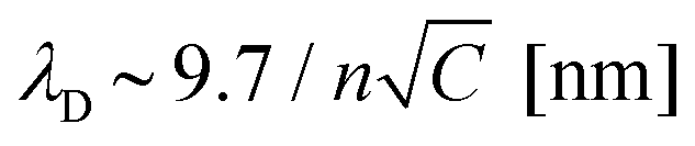 for aqueous solutions with ε = 80 at room temperature, where n is the ion valence and C the concentration in units of mM).47,48 Faradaic currents exponentially increase with the potential difference between that of the solid and of ions within a tunnelling distance (few nanometers). Consequently, in conventional electrochemistry the ultimate current for a given bias is achieved once the double layer is fully formed and its magnitude increases with decreasing λD.
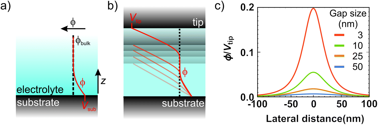 | ||
| Fig. 4 Tip-enabled local deposition mechanism in dilute electrolytes. Schematic representation of the potential drop at the solid–liquid interface for the general case of a metal electrode (a) and within the tip–substrate gap (b). When the gap size is smaller than twice the Debye screening length, the potential linearly decays with the distance. (c) Calculated potential profiles at 0.6 nm above the substrate for various gap sizes (3, 10, 25 and 50 nm) as obtained from the 2D Laplace's equation. We have considered a tip of 25 nm in radius held at a potential of Vtip and a grounded substrate. The potential is normalized to the tip bias. | ||
Considering oscillation amplitudes ranging from 10 to 300 nm, it becomes apparent that the typical electrode separation lies within the long screening length of the dilute electrolyte. In fact, due to incomplete screening the electrostatic attractive force is large enough to be sensed by the AFM. We observe this as an attractive force offset of ∼4 nN in the baseline when executing a single force curve on the substrate and toggling the applied potential at contact (ESI-6†). In the case where the electrode separation is ≤2λD (which has also been referred to as double layer cross-talk), the electrochemical conditions in the gap are not well-defined and may lead to unconventional electrochemistry. The double layer overlap between an STM tip and a metal substrate has been suggested to cause an enhanced local dissolution of the substrate while being held at a known potential, where no dissolution is expected.20,36,49 Particularly different in these works with respect to ours, is the much smaller gap sizes (<2 nm to ensure feedback from tunnelling current) and the unlimited access to the solid metal atoms for the oxidation reaction.
The interesting implication of incomplete screening in the gap is that the tip and substrate effectively form a capacitor. In other words, the ions inside the gap are subject to a (linear) potential profile between the electrodes purely defined by gap size and bias voltage (Fig. 4b). In the limiting case of no free charges in the gap, the potential can be calculated by solving Laplace's equation. Considering the plane of closest approach for a solvated ion (0.6 nm arising from the size of the water molecule48), the solution potential at the interface is raised by ∼5% of the tip voltage at a 10 nm gap size, and up to ∼20% at 3 nm, as illustrated in Fig. 4d. Since we typically use bias voltages up to ∼2 V, the unscreened tip perturbation can potentially increase the electrochemical potential of ions inside the gap by up to a few hundred mV through direct electrostatic interaction. This effect greatly enhances the local charge transfer, leading to local growth. However, the direct electrostatic interaction quickly disappears as the tip moves away from the substrate and/or upon the build-up of the double layer.
At small potentials, both the assembly and disassembly of the double layer are associated with the diffusion of ions from the bulk to the interface, and vice versa, through the diffuse layer over a time τD = λD2/D, with D being the diffusion coefficient.50 In standard electrochemistry, τD is of the order of ns. However, given the extended screening length in the dilute electrolyte, τD is 22 μs (33 μs) for the SO42− (Cu2+) ions (using DSO42− = 1.065 × 10⁻⁵ cm2 s−1, DCu2+ = 0.72 × 10⁻⁵ cm2 s−1), which is remarkably close to the contact time threshold for deposition found in Fig. 3c. The continuous full disruption of the EDL by the tip being in contact with the substrate for a time >τD facilitates the incomplete screening in the gap at each tapping cycle. Similar to potential-pulsed electrochemistry, the contact time or “off-time” results in electrochemical equilibrium by means of double layer relaxation. This equilibrium is then disturbed when the cantilever moves up, and the EDL reassembles again by ions moving into the tip–sample gap. Potential pulses at STM tips have led to confined electrochemical machining, atomic layer electrochemical deposition or control over crystallographic defect formation, among other phenomena.37,39,51,52
Although the proposed writing mechanism predicts that the local current increases with tip bias, we observe that the deposition is generally hampered at high potentials unless the gap size is small (Fig. 3). We believe that accelerated charge screening from field-enhanced ion transport reduces the total effective time for tip-induced double layer squeezing. Along this line, we suspect that access of ions into the gap becomes restricted for gap sizes smaller than 10 nm (see approach curves in ESI-5†). In this case, a higher driving potential is required to facilitate mass transport. This results in a balancing between the driving potential and the gap size, as observed in our measurements in Fig. 3b and c. Also, it seems that at high driving potentials the CT threshold for growth occurs at longer times. We suspect that steric effects may play a role, based on the fact that at high potentials or in highly concentrated electrolytes (such as ionic liquids), the double layer actually expands.53,54 In such a case, more time would be required to reach electrochemical equilibrium during the “off-time”.
Finally, we comment on the fact that higher concentrations hamper the local deposition within our available parameter window. Considering the discussion above, it is noteworthy that at just slightly higher concentrations, 10 μM, the improved screening power of the electrolyte results in the Debye screening length being about three times shorter (λD ∼50 nm). Double layer cross-talk and direct electrostatic interaction in less dilute electrolytes are therefore expected only at small oscillation amplitudes, where mass transport limitations become dominant. Further dilution of the electrolyte might broaden the deposition parameter window, but rapidly becomes impractical.
In summary, the writing mechanism requires a careful compromise between the tip–substrate electrostatic interaction (achieved by continuously disrupting the double layer and closely positioning the tip above the sample) while still allowing ion access. In our experiments, this occurs only in highly dilute electrolytes (<5 μM) with an extended Debye screening length combined with either: (a) oscillation amplitudes ∼25–50 nm, CT ∼100–150 μs and low drive potentials, or (b) small oscillation amplitudes (∼10 nm), long CT (>200 μs) and high drive potentials. While the latter conditions result in faster writing speeds (up to 3 × 10⁴ nm3 s−1), the former is best in terms of process efficiency, which considers the ratio between total charge transfer and local volume.
Based on the deposition mechanism described above, we suspect that only a small fraction of the non-contact time is responsible for the local deposition, reducing both the writing speed and process efficiency. In our system, the tip oscillation frequency is fixed at 2kHz and we obtain practical deposition rates in the order of 104 nm3 s−1, which is comparable to that for focused ion beam induced deposition.3 The writing speed, and consequently the process efficiency, may be optimised by tuning the tip oscillation frequency. Additionally, the overall process efficiency may also be improved by just reducing the substrate's surface area or by using a 4-electrode configuration, which fixes the substrate potential exactly at the Cu|Cu2+ equilibrium potential.
Regarding the writing resolution, further down-scaling is possible by the use of sharper tips considering that the observed resolution is of the size of the nominal tip diameter. Nowadays, conductive tips can be routinely fabricated with a diameter <10 nm. Sharper tips may also aid the deposition process by mitigating screening effects, due to the enhanced charge density and capacity of sharply curved metal surfaces.23
Conclusions
We have demonstrated the confined high-resolution direct additive writing of copper nanostructures by using a biased AFM tip in a dilute electrolyte, where the tip is in intermittent contact with the substrate through the oscillation of the cantilever. We find a particularly intriguing critical dependence of deposition on the tapping dynamics of the AFM and ion concentration. We propose a confinement mechanism that balances access of ions and shaping of the electrochemical potential in the tip–substrate gap. While this method is expected to be general for the electrochemical deposition of a variety of materials, opening up new routes for nanofabrication, probing local reactions through topography provides a way to understand the local dynamics and charge transfer at the electrical double layer, such as the Debye time.Methods
Sample and electrolyte preparation
The substrate consists of a Au film (∼ 50 nm thick) with a ∼5 nm Cr adhesion layer deposited by thermal evaporation on top of an n-type Silicon sample (Siegert Wafer) as a flat support. The solutions were prepared using CuSO4·5H2O powder (99.995%, from Sigma-Aldrich) in MilliQ® (18.2 MΩ cm) water. The low concentration electrolyte was prepared before every experiment from a 1 mM CuSO4(aq) stockpile and diluted (100–1000×) using fresh MilliQ water. Before preparing the dilute electrolyte, all containers were rinsed (5–10×), ultrasonicated, and rinsed again (5–10×) using fresh MilliQ water. Both the container and electrochemical cell only contained the dilute copper electrolytes, after initially cleaning them by an overnight soak in 1 M HCl. All experiments were carried out under ambient conditions inside a fume hood. Samples and the electrochemical cell were stored in a 1% humidity nitrogen environment.Electrochemistry
Our electrochemical system consists of an AFM nanoelectrode tip immersed in a filled electrochemical cell and connected to an external potentiostat, which controls and monitors potential and current. At positive potentials (tip vs. substrate), we expect the oxygen evolution reaction to occur at the tip and either copper reduction or hydrogen evolution at the sample. The electrochemical cell was homemade and consisted of Teflon™, made leak tight by an O-ring. Top-contacts were made by either attaching a wire connection directly to the sample edge, or by using a spring-loaded pin outside of the O-ring. Potential/current control and readout were done with a CH760E potentiostat. In all experiments, the system was connected in a 2-electrode fashion, by shorting the reference and counter electrode.Atomic force microscopy
The measurements and writing were performed using a Bruker Dimension Icon AFM, controlled through the Nanoscope software. The nanoelectrode AFM probes were obtained from Bruker (PeakForce SECM) and were electrically insulated except for the platinum coated apex, which has a diameter of ∼50 nm.42 The AFM spring constant was obtained for each cantilever (i) directly in the electrolyte, by doing a thermal tune at a distance of ∼1 mm from the substrate after obtaining the deflection sensitivity on the gold substrate inside the electrolyte, or (ii) before filling the cell using the thermal tune method in air at a distance of ∼1 mm from the substrate, after obtaining the deflection sensitivity on the gold substrate. The deflection sensitivity of the cantilever was then re-calibrated on the gold substrate, inside the electrolyte. The measured f0, Q, and used k are reported in ESI-7† as proposed in reference.55Ex situ topography and data in Fig. 1b, c, and 2 were obtained in air using ScanAsyst-air tips (Bruker, nominal tip radius 2 nm). In situ images and data in Fig. 1d and 3 were collected using the SECM tip, directly after deposition.Writing protocol
For writing, the tip follows a programmed trajectory (NanoScript) in the xy-plane with the PeakForce (PF) feedback enabled, while applying either a potential difference between the tip and the substrate (potentiostat) or forcing a fixed current through the tip (galvanostat). In all presented experiments, the PeakForce frequency was set to 2 kHz, other AFM parameters used are listed in the ESI.† Lift experiments where the tip is kept at a fixed distance above the substrate, as mentioned in the text, were done by initiating a Thermal Tune within the AFM software at a certain height.Data treatment
AFM images were treated by removing the polynomial background (first or second order) and removing image defects by aligning rows or removing scars using the Nanoscope Analysis and Gwyddion software.56 The volume data in Fig. 2 were defined as the bearing volume in the deposited lines, with a threshold value for each pixel set to two times the sample roughness. The height data in Fig. 3a were obtained by taking the average line profile of a written copper wire and fitting a Gaussian to obtain the height and full width half maximum as illustrated in ESI-8.† The volume in Fig. 3b was then taken to be the area of this fit multiplied by the length of the path. Fitting was done using the Origin 2017 software.Analytical model
We have considered a mirror charge at a distance of ‘gap size’ from the interface. Vtip is defined as the potential at a radial distance of 25 nm, and we have used the dielectric constant of water (80). We consider the substrate to be grounded with respect to the solution. This is a fair approximation given the much larger current density flowing through the tip.Conflicts of interest
There are no conflicts to declare.Acknowledgements
This work is part of the research program at the Netherlands Organisation for Scientific Research (NWO). Authors thank D. Ursem and the design and precision manufacturing departments at Amolf for their support. We also thank M. Valenti, I. Kolpakov and A. Polman for fruitful discussions.Notes and references
- S. M. Oja, Y. Fan, C. M. Armstrong, P. Defnet and B. Zhang, Anal. Chem., 2016, 88, 414 CrossRef CAS PubMed.
- G. Staikov, Nanoscale, 2016, 8, 13880 RSC.
- L. Hirt, A. Reiser, R. Spolenak and T. Zambelli, Adv. Mater., 2017, 29, 1604211 CrossRef PubMed.
- B. Lam, W. Zhou, S. O. Kelley and E. H. Sargent, Nat. Commun., 2015, 6, 6940 CrossRef CAS PubMed.
- T. A. Schaedler, A. J. Jacobsen, A. Torrents, A. E. Sorensen, J. Lian, J. R. Greer, L. Valdevit and W. B. Carter, Science, 2011, 334, 962–966 CrossRef CAS PubMed.
- J. K. Gansel, M. Thiel, M. S. Rill, M. Decker, K. Bade, V. Saile, G. Von Freymann, S. Linden and M. Wegener, Science, 2009, 325, 1513–1516 CrossRef CAS PubMed.
- A. Reiser, M. Lindén, P. Rohner, A. Marchand, H. Galinski, A. S. Sologubenko, J. M. Wheeler, R. Zenobi, D. Poulikakos and R. Spolenak, Nat. Commun., 2019, 10, 1853 CrossRef PubMed.
- J. Hu and M.-F. Yu, Science, 2010, 329, 313–317 CrossRef CAS PubMed.
- L. Hirt, S. Ihle, Z. Pan, L. Dorwling-carter, A. Reiser, J. M. Wheeler, R. Spolenak, J. Vörös and T. Zambelli, Adv. Mater., 2016, 28, 2311–2315 CrossRef CAS PubMed.
- D. Momotenko, A. Page, M. Adobes-vidal and P. R. Unwin, ACS Nano, 2016, 10, 8871 CrossRef CAS PubMed.
- M. Ghatkesar, H. Garza, F. Heuck and U. Staufer, Micromachines, 2014, 5, 954–1001 CrossRef.
- B. Maynor, Y. Li and J. Liu, Langmuir, 2001, 2575–2578 CrossRef CAS.
- J. H. Je, J. Kim and J. Jaworski, Small, 2017, 13, 1600137 CrossRef PubMed.
- F. Wang, H. Xiao and H. He, Sci. Rep., 2016, 6, 26270 CrossRef CAS PubMed.
- J. R. Lagraff and A. A. Gewirth, J. Phys. Chem., 1994, 98, 11246–11250 CrossRef CAS.
- C. Obermair, A. Wagner and T. Schimmel, Beilstein J. Nanotechnol., 2011, 2, 659–664 CrossRef CAS PubMed.
- S. E. Vasko, A. Kapetanovi, V. Talla, M. D. Brasino, Z. Zhu, A. Scholl, J. D. Torrey and M. Rolandi, Nano Lett., 2011, 11, 2386–2389 CrossRef CAS PubMed.
- R. Garcia, A. W. Knoll and E. Riedo, Nat. Nanotechnol., 2014, 9, 577–587 CrossRef CAS PubMed.
- W. Schindler, D. Hofmann and J. Kirschner, J. Electrochem. Soc., 2001, 148, 124 CrossRef.
- S. G. Garcia, D. R. Salinas, C. E. Mayer, W. J. Lorenz and G. Staikov, Electrochim. Acta, 2003, 48, 1279–1285 CrossRef CAS.
- G. Wittstock, M. Burchardt, S. E. Pust, Y. Shen and C. Zhao, Anal. Methods, 2007, 46, 1584–1617 CAS.
- S. Sarkar, S. C. S. Lai and S. G. Lemay, Micromachines, 2016, 7, 81 CrossRef PubMed.
- M. Liu, Y. Pang, B. Zhang, P. De Luna, O. Voznyy, J. Xu, X. Zheng, C. T. Dinh, F. Fan, C. Cao, F. P. G. De Arquer, T. S. Safaei, A. Mepham, A. Klinkova, E. Kumacheva, T. Filleter, D. Sinton, S. O. Kelley and E. H. Sargent, Nature, 2016, 537, 382–386 CrossRef CAS PubMed.
- S. S. Lee, P. Fenter, K. L. Nagy and N. C. Sturchio, Nat. Commun., 2017, 8, 15826 CrossRef PubMed.
- M. Hugelmann and W. Schindler, Surf. Sci., 2003, 541, 643 CrossRef.
- L. Collins, J. I. Kilpatrick, S. V. Kalinin and B. J. Rodriguez, Rep. Prog. Phys., 2018, 81, 086101 CrossRef PubMed.
- R. Hiesgen, D. Eberhardt and D. Meissner, Surf. Sci., 2005, 597, 80–92 CrossRef CAS.
- R. L. Harniman, D. Plana, G. H. Carter, K. A. Bradley, M. J. Miles and D. J. Fermín, Nat. Commun., 2017, 8, 971 CrossRef PubMed.
- D. Martin-jimenez, E. Chacon, P. Tarazona and R. Garcia, Nat. Publ. Gr., 2016, 7, 12164 CAS.
- T. Fukuma, K. Kobayashi, K. Matsushige and H. Yamada, Appl. Phys. Lett., 2005, 87, 034101 CrossRef.
- K. Umeda, K. Kobayashi, T. Minato and H. Yamada, Phys. Rev. Lett., 2019, 122, 116001 CrossRef CAS PubMed.
- J. J. Kuna, S. A. Contera, E. Tosatti and F. Stellacci, Nat. Nanotechnol., 2010, 5, 401 CrossRef PubMed.
- I. Siretanu, D. Ebeling, M. P. Andersson, S. L. S. Stipp, A. Philipse, M. C. Stuart, D. Van Den Ende and F. Mugele, Sci. Rep., 2014, 4, 4956 CrossRef CAS PubMed.
- K. Hirata, T. Kitagawa, K. Miyazawa, T. Okamoto, A. Fukunaga, C. Takatoh and T. Fukuma, Nanoscale, 2018, 10, 14736 RSC.
- D. Perry, R. Al Botros, D. Momotenko, S. L. Kinnear, P. R. Unwin and P. E. T. Al, ACS Nano, 2015, 9, 7266–7276 CrossRef CAS PubMed.
- Z. Xie and D. M. Kolb, J. Electroanal. Chem., 2000, 481, 177–182 CrossRef CAS.
- R. Schuster, V. Kirchner, P. Allongue and G. Ertl, Science, 2000, 289, 98–101 CrossRef CAS PubMed.
- L. Collins, S. Jesse, J. I. Kilpatrick, A. Tselev, O. Varenyk, M. B. Okatan, S. A. L. Weber, A. Kumar, N. Balke, S. V. Kalinin and B. J. Rodriguez, Nat. Commun., 2014, 5, 3871 CrossRef CAS PubMed.
- R. Schuster, V. Kirchner, X. H. Xia, A. M. Bittner and G. Ertl, Phys. Rev. Lett., 1998, 80, 5599–5602 CrossRef CAS.
- R. Widmer and H. Siegenthaler, Electrochem. Commun., 2005, 7, 421–426 CrossRef CAS.
- R. T. Pötzschke, G. Staikov, W. J. Lorenz and W. Wiesbeck, J. Electrochem. Soc., 1999, 146, 141–149 CrossRef.
- Z. Huang, P. De Wolf, R. Poddar, C. Li, A. Mark, M. R. Nellist, Y. Chen, J. Jiang, G. Papastavrou, S. W. Boettcher, C. Xiang and B. S. Brunschwig, Microsc. Today, 2016, 18 CrossRef CAS.
- D. M. Kolb and F. C. Simeone, Electrochim. Acta, 2005, 50, 2989–2996 CrossRef CAS.
- S. Seol, A. R. Pyun, Y. Hwu, G. Margaritondo and J. H. Je, Adv. Funct. Mater., 2005, 15, 934 CrossRef CAS.
- J. D. Madden and I. W. Hunter, J. Microelectromech. Syst., 1996, 5, 1057 CrossRef.
- R. A. Said, Nanotechnology, 2003, 14, 523 CrossRef CAS.
- T. I. Quickenden and Q. Xu, J. Electrochem. Soc., 1996, 143, 1248–1253 CrossRef CAS.
- R. G. Compton, Understanding voltammetry, Imperial College Press, 2011 Search PubMed.
- J. W. Yan, Z. X. Xie, Z. X. Cao, C. J. Zhou, J. Y. Kang and B. W. Mao, Chem. Phys. Lett., 2003, 373, 575 CrossRef CAS.
- M. Z. Bazant, K. Thornton and A. Ajdari, Phys. Rev. E: Stat., Nonlinear, Soft Matter Phys., 2004, 70, 0215006 CrossRef PubMed.
- Y. Liu, D. Gokcen, U. Bertocci and T. P. Moffat, Science, 2012, 338, 1327–1330 CrossRef CAS.
- S. Daryadel, A. Behroozfar, S. R. Morsali, S. Moreno, M. Baniasadi, J. Bykova, R. A. Bernal and M. Minary-jolandan, Nano Lett., 2018, 18, 208 CrossRef CAS PubMed.
- M. Z. Bazant, M. S. Kilic, B. D. Storey and A. Ajdari, New J. Phys., 2009, 11, 075016 CrossRef.
- M. A. Gebbie, A. M. Smith, H. A. Dobbs, A. A. Lee, G. G. Warr, X. Banquy, M. Valtiner, M. W. Rutland, J. N. Israelachvili, S. Perkin and R. Atkin, Chem. Commun., 2017, 53, 1214–1224 RSC.
- J. E. Sader, R. Borgani, C. T. Gibson, D. B. Haviland, M. J. Higgins, I. Jason, J. Lu, P. Mulvaney, C. J. Shearer, A. D. Slattery, P. Thorén, J. Tran, J. E. Sader, R. Borgani, C. T. Gibson, D. B. Haviland, M. J. Higgins, J. I. Kilpatrick, J. Lu, P. Mulvaney, C. J. Shearer, A. D. Slattery, P. Thorén, J. Tran, H. Zhang, H. Zhang and T. Zheng, Rev. Sci. Instrum., 2016, 87, 093711 CrossRef PubMed.
- D. Necas and P. Klapetek, Cent. Eur. J. Phys., 2012, 10, 181 Search PubMed.
Footnote |
| † Electronic supplementary information (ESI) available. See DOI: 10.1039/c9nr05574f |
| This journal is © The Royal Society of Chemistry 2019 |