
 Open Access Article
 This Open Access Article is licensed under a Creative Commons Attribution-Non Commercial 3.0 Unported Licence
Layer-dependent dielectric and optical properties of centimeter-scale 2D WSe2: evolution from a single layer to few layers†
Honggang
Gu‡
 a,
Baokun
Song‡
a,
Mingsheng
Fang
a,
Yilun
Hong
b,
Xiuguo
Chen
a,
Hao
Jiang
a,
Wencai
Ren
*b and
Shiyuan
Liu
*a
a,
Baokun
Song‡
a,
Mingsheng
Fang
a,
Yilun
Hong
b,
Xiuguo
Chen
a,
Hao
Jiang
a,
Wencai
Ren
*b and
Shiyuan
Liu
*a
aState Key Laboratory of Digital Manufacturing Equipment and Technology, Huazhong University of Science and Technology, Wuhan 430074, Hubei, China. E-mail: shyliu@hust.edu.cn
bShenyang National Laboratory for Materials Science Institute of Metal Research Chinese Academy of Sciences, Shenyang 110016, P. R. China. E-mail: wcren@imr.ac.cn
First published on 2nd September 2019
Abstract
Two-dimensional (2D) materials usually exhibit interesting layer-dependent dielectric and optical properties, which play important roles in structure optimization and performance improvement of related devices. Recently, 2D WSe2 has attracted considerable attention in atomically thin electronics and optoelectronics, due to its exotic photoelectric properties. In this paper, high-quality, continuous, and centimeter-scale 2D WSe2 with different layers on a sapphire substrate are prepared by an ultrafast ambient-pressure chemical vapor deposition method. We comprehensively investigate the evolution of the layer-dependent dielectric and optical properties of 2D WSe2 from a single layer to five layers by spectroscopic ellipsometry over an ultra-broad energy range (0.73–6.42 eV). We identify the critical points (CPs) in the dielectric function spectra of 2D WSe2 with different layers, and reveal physical origins of the corresponding optical transitions at these CPs by the CP analysis method and first-principles calculations. Results demonstrate that the center energies of these CPs exhibit intriguing layer-dependencies, which can be interpreted as the alternative domination of the decreasing exciton binding energy and the striking band renormalization. For the first time, we found that the imaginary part of the dielectric function of WSe2 at these CPs exhibits a valley-like shape versus the layer number, and the bottom appears at 3-layers. This non-monotonic evolution is explained as a competition between the layer-dependent decrease of the exciton effect and the layer-dependent increase of the joint density of states.
1. Introduction
Recently, a two-dimensional transition metal dichalcogenide (2D-TMDC) WSe2 has attracted considerable attention in atomically thin electronics and optoelectronics due to its exotic photoelectric properties, such as layer-modulated bandgaps,1 moderate mobility (∼200 cm2 V−1 s−1), a high on–off ratio (108),2,3 and a prominent spin–orbit coupling (SOC) effect.4 The use of 2D WSe2, in the forms of intrinsic (doped) 2D WSe2 and customized heterostructures hybridized with other 2D materials, significantly improves the performances of related optoelectronic devices and endows them with many distinctive properties.5–8 Performances of these optoelectronic devices strongly depend on the intrinsic dielectric and optical properties (usually described with the dielectric function and the complex refractive index, respectively, which can be converted to each other) of 2D WSe2 and these properties usually exhibit obvious layer-dependencies.9–11 Therefore, comprehensively investigating the dielectric and optical properties of WSe2 with different layers (L) and revealing the underlying physical mechanisms are instructive to the design and optimization of these novel devices.12Typical experimental techniques used to study the optical properties of 2D WSe2 mainly include photoluminescence (PL) spectroscopy,9,13 Raman spectroscopy,13,14 and reflection (transmission and absorption) spectroscopy.9,10 To some extent, these techniques can indeed help obtain some physicochemical information of 2D WSe2, such as the optical bandgap, lattice structure, absorption characteristic, etc. However, the intrinsic dielectric and optical parameters of 2D WSe2, including the dielectric function (ε = ε1 − iε2, where ε1 and ε2 refer to the real part and imaginary part of the dielectric function) and the complex refractive index (N = n – ik, where n and k refer to the refractive index and the extinction coefficient, respectively), cannot be derived from these spectra directly. So far, experimental studies on the layer-dependent dielectric and optical parameters of 2D WSe2 have scarcely been reported. Commonly used techniques to determine the dielectric function and complex refractive index of 2D WSe2 include the reflection (or absorption) spectrum method,15 differential reflection (or transmission) spectrum method,16 scattering-type scanning near-field optical microscopy (s-SNOM),17–20 and ellipsometry.21–24 With the reflection (or absorption) spectrum method, Li et al. obtained the dielectric function of the monolayer WSe2 over an energy range of 1.5–3.0 eV by combining a Kramers–Kronig (K–K) constrained variational analysis.15 This method depends on the absolute detected light intensity, which can be easily affected by the experimental environment. Moreover, to obtain both the real and imaginary parts of the dielectric function, the K–K relationship needs to be applied, which introduces some inevitable errors to the final results.25 Morozov et al. simultaneously measured the frequency-dependent reflection (transmission) spectra and corresponding differential spectra of monolayer WSe2, and extracted the dielectric function without employing the K–K relationship.16 Although this method avoids the use of the K–K relationship, it requires repeated experiments, longer measurement time, and expensive subsequent calculations to obtain accurate results. s-SNOM is sensitive to the optical anisotropy in 2D materials, and can be used to determine the dielectric tensor of a thin film.18 It has been recently developed to probe the optical anisotropy in 2D van der Waals materials,18,19 and to investigate the plasmonic and polaritonic properties in 2D materials, metamaterials, quantum materials, etc.20 Compared with the techniques discussed above, ellipsometry detects the polarization state changes of polarized light before and after reaction (reflection or transmission) with the samples, and the dielectric and optical parameters of 2D materials can be accurately extracted from the ellipsometric spectra without any additional functions.26 Eichfeld et al. measured the ellipsometric spectra of WSe2 films with different thicknesses and obtained their complex refractive indices over a wavelength range of 200–1000 nm.21 Similarly, Diware et al. extracted the dielectric functions and thicknesses of 1L and 3L WSe2 from the measured ellipsometric spectra by using multilayer optical calculations with appropriate optical models.23,24 However, the existing ellipsometric studies on 2D WSe2 failed to reveal the evolution of layer-dependent dielectric and optical properties due to the lack of high-quality materials with continuous layers. Moreover, the physical mechanisms behind these properties of 2D WSe2 have not been understood yet. In addition to the above experimental studies, some researchers carried out investigations on the dielectric and optical properties of 2D WSe2 on the basis of theoretical calculations.27,28 By using the first-principles calculations, Johari et al. gave convincing explanations for the layer-dependent dielectric properties of WSe2 by analyzing the calculated electron energy loss spectra.27 Kumar et al. also studied the relationship between the dielectric response and the layer number of WSe2 by means of ab initio calculations.28 However, these theoretical results lack sufficient experimental verification.
In this paper, we prepared high-quality, continuous, and centimeter-scale layer-gradient 2D WSe2 specimens on sapphire by an ultrafast ambient-pressure chemical vapor deposition method. The evolution of the dielectric and optical properties of 1–5L WSe2 is comprehensively investigated by spectroscopic ellipsometry over an energy range of 0.73–6.42 eV, and the physical mechanisms behind these layer-dependent properties are revealed. A systematic method based on the critical point (CP) analysis and first-principles calculations is proposed to identify the spatial positions in the Brillouin zone (BZ), energy bands, and carrier types of the optical transitions occurring at the CPs of 2D WSe2. By using the proposed method, up to eight critical points (CPs) A–H are distinguished in the in-plane dielectric function spectra of 2D WSe2, and their corresponding transitions are further identified from the band structures and projected density of states (PDOS). We find that the center energies of these CPs exhibit intriguing layer-dependencies, and interpret them as the competition between the exciton binding energy and the striking shrinkage of energy bands. Results demonstrate that the imaginary part of the in-plane dielectric function at these CPs exhibits a valley-like shape versus the layer number of WSe2, and the valley bottom appears at 3L. We explain the non-monotonous evolution of the layer-dependent dielectric function as a joint contribution from the exciton effect and the joint density of states (JDOS).
2. Experimental section
2.1. Preparation of centimetre-scale 2D WSe2
High-quality, continuous, centimeter-scale 2D WSe2 films were grown on gold foil (99.95 wt%, 100 μm thick, 2 × 1 cm2 size, Alfa Aesar) by an ultrafast ambient-pressure chemical vapor deposition method using WO3 powder and Se pellets as precursors (Fig. 1a). After growth, the 2D WSe2 samples were transferred onto polished sapphire substrates (1 cm × 1 cm) with a nondestructive electrochemical bubbling method. The detailed growth process and transfer procedure can be found in our previous publications.29,30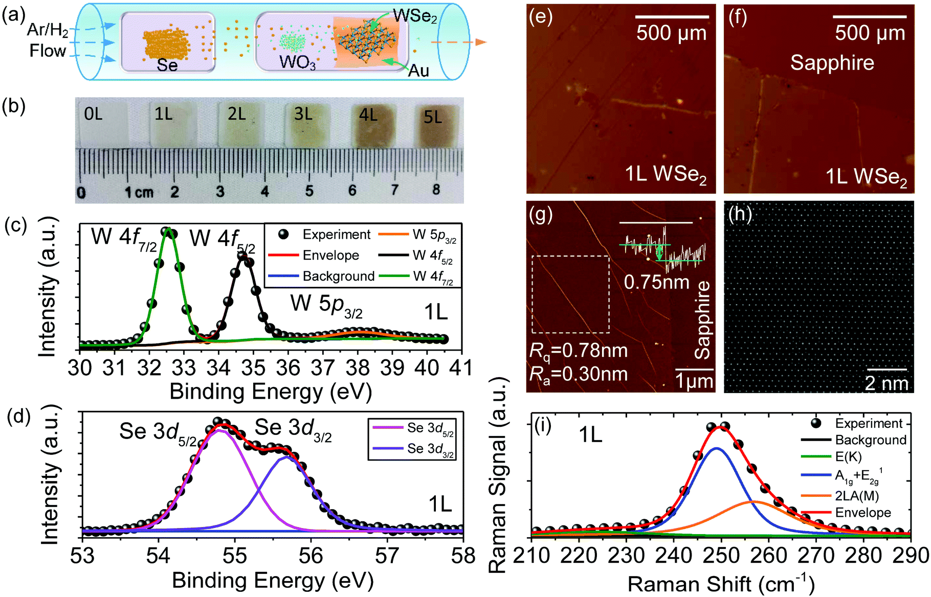 | ||
| Fig. 1 (a) Schematic diagram of the ultrafast ambient-pressure CVD method. (b) Photographs of 0–5L WSe2 on the sapphire substrates. (c and d) Measured XPS spectra and the corresponding peak-differentiation-imitating analysis results for monolayer WSe2. (e and f) Optical images of monolayer WSe2 transferred on a sapphire substrate. (e) Center region. (f) Edge region. (g) AFM image of monolayer WSe2, and the high profiles across the white solid line. The white box indicates the area that was used to evaluate the surface roughness. (h) HAADF-STEM image of monolayer WSe2. (i) Typical Raman spectrum of monolayer WSe2; the wavelength of the detection laser is 532 nm. | ||
2.2. Characterization of 2D WSe2
An Escalab 250Xi X-ray photoelectron spectrometer with an Al-Kα radiation source (1486.6 eV) was used to analyze the elemental composition of the WSe2 films. The surface roughness and thicknesses of the WSe2 films were characterized by atomic force microscopy (AFM) (Bruker Dimension ICON). High-angle annular dark field scanning transmission electron microscopy (HAADF-STEM) imaging was performed on an aberration-corrected and monochromated transmission electron microscope (TEM) (Nion UltraSTEM 100) operating at 60 kV. The Raman spectra of the WSe2 specimens were recorded by using an argon ion laser Raman spectrometer (LabRAM HR800, Horiba Jobin Yvon) with a 532 nm line. A commercial spectroscopic ellipsometer (ME-L Mueller matrix ellipsometer, Wuhan Eoptics Technology Co., Wuhan, China) was used to investigate the dielectric and optical properties of WSe2 specimens, whose applicable energy region covers 0.73–6.42 eV,25,27,31,32 and an incident angle of 65° is optimally selected in the ellipsometric measurement.2.3. First-principles calculations
All the first-principles calculations were performed with the Vienna ab initio package (VASP v5.4.1).33 The structures were optimized with the PBE functional based on PAW pseudopotentials.34 Periodic images of monolayers and multilayers were separated by 15 Å of vacuum, and van der Waals corrections vdw-D2 were taken into consideration. The criterion for the convergence of forces and total energy was set to 0.01 eV Å−1 and 10−5 eV. The electronic properties were calculated with the HSE06 hybrid functional based on PAW pseudopotentials.35 In all cases, the kinetic energy cutoff was set at 700 eV and the BZ sampled with an 8 × 8 × 1 Γ-centered k-point mesh for monolayer WSe2 and an 8 × 8 × 2 Γ-centered k-point mesh for multilayer WSe2. The calculations were performed taking the SOC effect into consideration.3. Results and discussion
Fig. 1b clearly shows that the optical contrast gradually increases from the bare sapphire substrate to 5L WSe2. As shown in Fig. 1c and d, we performed X-ray photoelectron spectroscopy (XPS) on monolayer WSe2 and each XPS peak could be well fitted with one Voigt function, implying that only one tungsten- or selenium-containing chemical species exists at the surface. Moreover, the center energies of these XPS peaks agree well with a previous experimental report.36 Optical images of the central and edge regions of the monolayer WSe2 specimen (see Fig. 1e and f) show that the WSe2 film has uniform thickness. AFM measurements show that monolayer WSe2 has a thickness of 0.75 nm and low surface roughness (Fig. 1g). The HAADF-STEM image shows a clear hexagonal lattice structure without vacancies and defects (Fig. 1h). As shown in Fig. 1i, by analyzing the Raman spectrum of monolayer WSe2, four characteristic Raman modes can be distinguished, including first-order out-of-plane mode A1g, first-order in-plane mode E2g1, overtone of the long acoustic phonon branch at the M point (we refer to it as 2LA(M)), and a phonon mode of the E-symmetry optical branch at the K point of the BZ (named E(K)). The center frequencies of these Raman modes agree with those of the mechanically exfoliated monolayer WSe2 flakes.14,37 All these results confirm that our CVD-grown WSe2 is a high-quality monolayer film. The XPS results (Fig. S1†), thicknesses (Fig. S2 and Table S1†), surface roughness (Fig. S2†), and Raman spectra (Fig. S3†) of 2–5L WSe2 films are summarized in the ESI.†To perform the ellipsometric analysis on the 2D WSe2 specimens, a vertical stacking optical model (Fig. 2a) is constructed to approximately embody the optical structure of the WSe2 film on the sapphire substrate. The optical model contains 4 layers including the ambient air layer, the WSe2 film layer, a Bruggeman interlayer38 (50% WSe2 and 50% sapphire), and the sapphire substrate. The interlayer is a unique consideration of the surface roughness of the sapphire substrate. The transferred WSe2 film gradually adheres to the microprofile of the sapphire during the annealing process, forming an ultrathin transition layer. The Bruggeman interlayer is able to describe the properties of the transition layer to some extent, improving the final ellipsometric analysis results.39,40 Actually, layered 2D WSe2 can be regarded as an optical uniaxial material, whose dielectric properties can be described by a second-order dielectric tensor ε = diag(εo, εo, εe). Here, εo and εe denote the ordinary and the extraordinary dielectric functions, respectively. It should be noted that we use a minus sign in front of the imaginary parts of the dielectric functions, i.e., εo = εo1 − iεo2 and εe = εe1 − iεe2, and we take the same sign convention for the complex refractive indices. As shown in Fig. 2a, the direction of εe is perpendicular to the surface of 2D WSe2 (parallel to the z-axis of the instrument coordinate system), and εo lies in the surface of 2D WSe2 (x-o-y plane). Thus, in this work, εo(εe) also refers to the in-plane (out-of-plane) dielectric function of 2D WSe2. To physically embody the dielectric properties of 2D WSe2 over the concerned energy range, εo is parameterized using a combined classical oscillator model, including 3 Cody–Lorentz oscillators and 5 Lorentz oscillators, and εe is parameterized with a Tauc–Lorentz oscillator.41 These oscillators can effectively describe the quasiparticle transitions occurring at the semiconductors.38,42 Based on the established optical model and dielectric model, theoretical ellipsometric spectra (Ψ(E), Δ(E)) of the WSe2 films can be calculated using the optical interference theory in multilayer films.38 Then, the dielectric functions and thicknesses of the WSe2 films can be simultaneously extracted by fitting the measured ellipsometric spectra with theoretically calculated ones. Analysis results (Fig. 2b and Fig. S4†) exhibit excellent goodness of fit. Further information on the ellipsometric analysis aiming at 2D materials is available in our previous reports.25 It should be noted that although sapphire is also a uniaxial crystal, considering the extremely weak birefringence (∼10−3) over the concerned spectral range,43 the optical anisotropy in the sapphire substrate is neglected in the ellipsometric analysis for convenience.
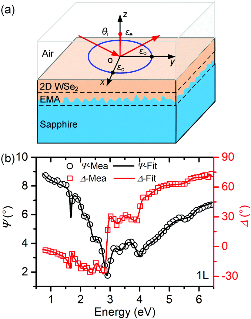 | ||
| Fig. 2 (a) Optical model of the 2D WSe2 film on the sapphire substrate, and the geometric relationships between the instrument coordinate system (x-o-y) and the dielectric functions. The incident angle θi = 65°. (b) Ellipsometric analysis results for monolayer WSe2. | ||
Since the thickness of the 2D WSe2 film we used is severely limited (<3.5 nm), the out-of-plane dielectric functions may contribute trivially to the optical response in ellipsometric measurement due to the difficulty in exciting the vertical dipole.44,45 In addition, the 2D WSe2 film in this work is polycrystalline, in which the assumption of optical anisotropy is not strict.44 The above two reasons may make the extracted out-of-plane dielectric function less stable and reliable. More importantly, the in-plane dielectric functions contain many more features than the out-of-plane dielectric functions, which can help us reveal more intrinsic optical and dielectric properties as well as the evolution of 2D WSe2. Thus, in this work, we will mainly focus on the layer-dependencies that the in-plane dielectric functions exhibit.
The in-plane dielectric functions and complex refractive indices of 1–5L WSe2 films over the concerned spectral range (0.73–6.42 eV) are plotted in Fig. 3a and b. Both real parts (εo1) (Fig. 3a) and imaginary parts (εo2) (Fig. 3b) of the in-plane dielectric function spectra for the WSe2 films present intricate layer-dependencies over the whole spectral range. It can be interpreted as the externalization related to the quasiparticle transitions, including normal optical transitions, peculiar exciton and trion transitions, etc. These transitions are closely related to the band structures of the materials. In 2D materials, the band structure is sensitive to the geometric size, especially the layer number, due to the prominent quantum confinement effect in the vertical direction. Specifically, the layer-dependent band structure of 2D WSe2 is the direct physical origin of the size effect exhibited in the dielectric function spectra. Up to eight CPs can be clearly distinguished in the in-plane dielectric function spectra as labeled by uppercase A–H in Fig. 3b, and their magnitudes and shapes are different from each other. For the four low-energy CPs (A–D), they present relatively larger magnitudes and narrower full widths at half maximum (FWHMs) compared with those of high-energy CPs E–H. These phenomena suggest that the transitions associated with the low-energy CPs may be relatively explicit and understandable. In other words, the transitions requiring higher energy to excite are restricted to some extent. In contrast, the broader FWHMs and the weaker intensities of high-energy CPs E–H imply that the transition behaviors related to these CPs are likely to be multifarious and competitive. It is worth noting that the CPs of monolayer WSe2 are sharper compared with those of multilayer WSe2, which can be understood as a lack of interlayer interactions in the monolayer material and the transitions associated with the out-of-plane direction are limited to an intralayer.9 The in-plane complex refractive indices of 1–5L WSe2 can be calculated from the in-plane dielectric functions according to the formula N2 = ε, and the results are presented in Fig. 3c and d. When the excitation energy is larger than 3 eV, the refractive index no of monolayer WSe2 is smaller than that of multilayer WSe2, while the extinction coefficient κo of monolayer WSe2 is larger than that of multilayer WSe2. The former phenomenon can be explained as the absence of interlayer interactions in monolayer WSe2. The latter can be attributed to the significantly enhanced excitonic behavior induced by the quantum confinement effect, which is expected to increase the absorption of the excitation energy.
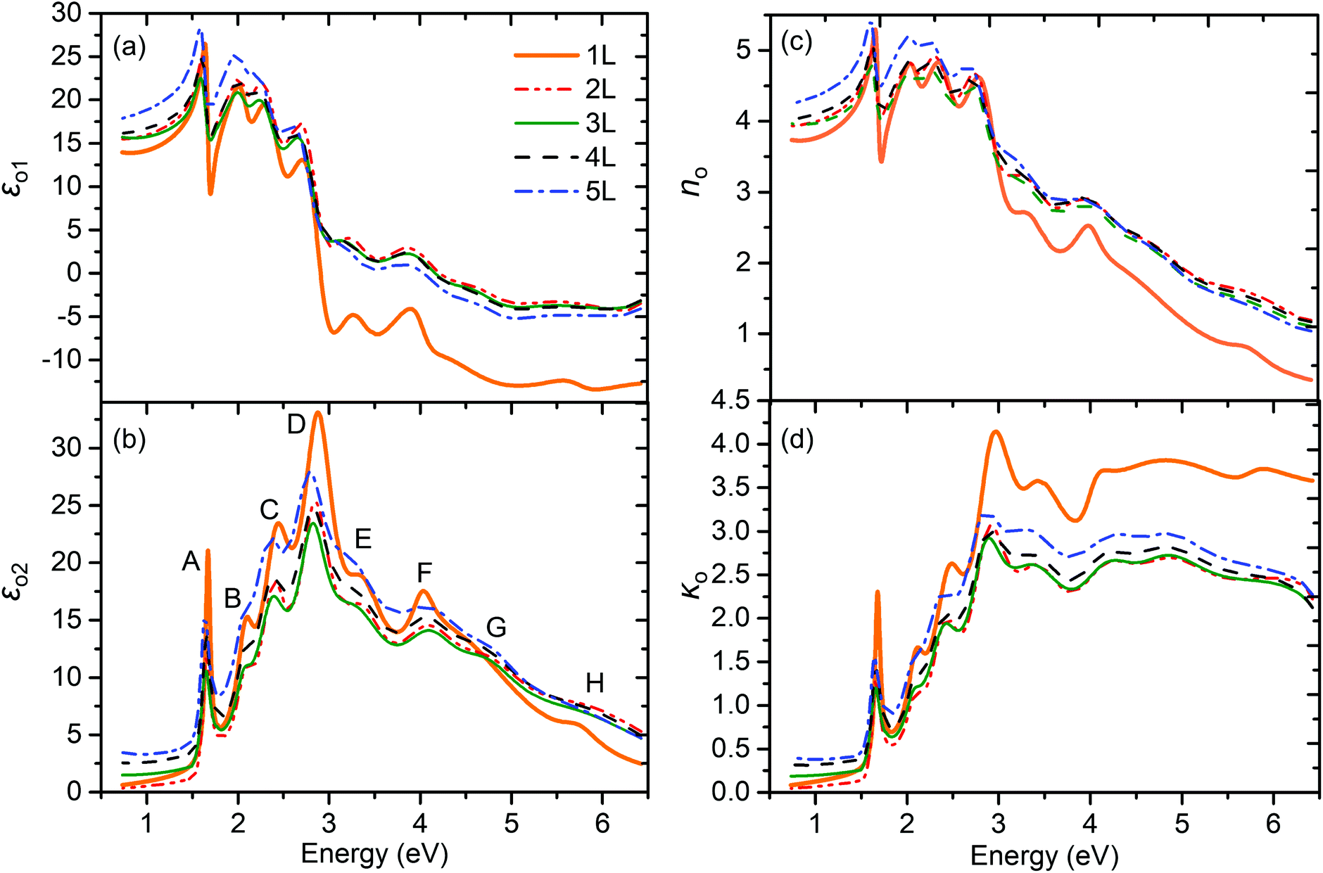 | ||
| Fig. 3 In-plane dielectric function spectra of 1–5L WSe2 measured using SE. (a) Real part εo1. (b) Imaginary part εo2. In-plane complex refractive index spectra of 1–5L WSe2 films. (c) Refractive index no. (d) Extinction coefficient κo. | ||
To further identify the physical origins of these optical transitions occurring at the CPs, we propose a systematic and analytical method by combining the CP analysis and the first-principles calculations. The proposed method has the ability to determine the spatial positions, energy bands, and carrier types of the transitions occurring at a specific CP. Firstly, the CP analysis method is applied to precisely determine the parameters of CPs, and meanwhile the first principles method is adopted to calculate the band structure and PDOS. The energy differences between the CBs and VBs (EC–V) are calculated based on the band structure. Then, these results are drawn together in a figure in a specific sequence, in which the CP analysis results, the energy differences EC–V, the band structure, and the PDOS are in the lower right corner, lower left corner, upper left corner and upper right corner, respectively. What's more, the EC–V is a bond linking the CPs and the band structure, and the EC–V subfigure is carefully aligned with the CPs and the band structure subfigures according to the energy axis and the momentum space, respectively. Also, the band structure subfigure is aligned with the PDOS subfigure according to the energy axis. Finally, the transitions occurring at the CPs are precisely identified according to the following steps.
(1) Equal-energy lines (EELs) are drawn throughout the CPs and the EC–V subfigures according the center energies of the CPs. The tangent points between EELs and the EC–V curves can be regarded as the transition positions. This is because the JDOS at the tangent point is singular, where the transition strength reaches an extreme value. The JDOS can be expressed as46
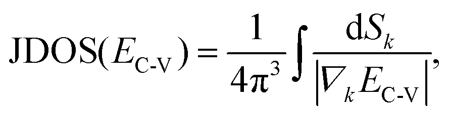 | (1) |
(2) Equal-momentum lines (EMLs) are drawn throughout the EC–V and the band structure subfigures to distinguish the energy bands involved in the transitions of the CPs.
(3) EELs are drawn throughout the band structure and the PDOS subfigures to figure out the specific carrier types responsible for the transitions.
Based on the proposed method, the underlying mechanisms of the transitions at the CPs of 2D WSe2 with different layers can be revealed. Taking monolayer WSe2 as an example, we performed first-principles calculations on the band structures (Fig. 4a) and the PDOS (Fig. 4b), and the CP analysis on the in-plane dielectric function spectra (Fig. 4d). Furthermore, the energy differences (EC–V) between the first four CBs and the first four VBs are evaluated and presented in Fig. 4c. Detailed analysis procedures for other WSe2 specimens can be found in the ‘Critical point analysis’ and ‘Transitions of 2–5L WSe2’ parts. Analysis results are presented in Fig. S5 and Table S2 of the ESI.†
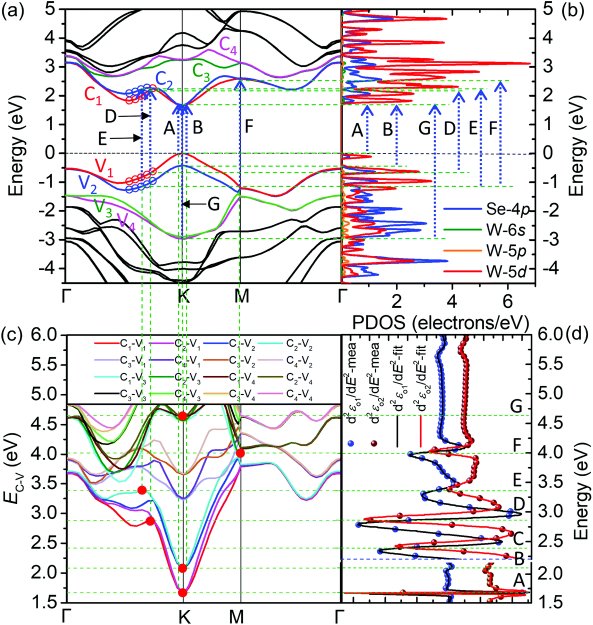 | ||
| Fig. 4 (a and b) Band structure and PDOS of monolayer WSe2 obtained from the first-principles calculations. (c) Energy differences EC–V between the first four CBs and the first four VBs of monolayer WSe2. (d) CP analysis result of monolayer WSe2. | ||
The specific spatial positions in the BZ, energy bands and carrier types of the transitions occurring at the CPs for 2D WSe2 can be identified by drawing EELs (green dashed lines throughout Fig. 4c and d and Fig. 4a and b) and EMLs (green dashed lines throughout Fig. 4a and c). The red dots in Fig. 4c represent the transition positions in the BZ, and the blue dashed lines in Fig. 4a and b mark out the specific energy bands and carrier types involved in the transitions. Specifically, the CPs A and B are associated with the direct transitions between the maxima of splitting VBs (V1 and V2) and the minimum of the CB (C1) at the K point of the BZ. The VB splitting phenomenon is mainly caused by the intralayer SOC effect.47,48 The origins of CPs D and E can be assigned to the transitions from V1(V2) to C1(C2) respectively, whose spatial positions may cover the range from 0.54 Γ–K to 0.74 Γ–K in the BZ (the region identified by red and blue open circles in Fig. 4a). In this interval, V1(V2) is almost parallel to C1(C2), and the striking band nesting leads to a prominent increase of the transition strength.49 The multiple direct transitions from V1/V2 to C1/C2 at the M point in the BZ make major contribution to the formation of the CP F. The broad CP G corresponds to the direct transitions that occur between the V3/V4 to the CB minimum at the K point in the BZ. Above the CP G, there exists a rarely reported high-energy and broad CP H at about 5.9 eV. We conjecture that it may be relevant to the multiplicate transitions from V1/V2 to the higher CBs. It should be pointed out that since the strength is extremely weak and the center energy may be beyond the spectral range of SE, we failed to extract detailed parameters of CP H exactly. In addition, due to the absence of a definite tangent point as presented in Fig. 4c, we cannot clearly identify the CP C using the proposed method. In the light of the band nesting phenomenon as discussed above, we think that the direct transitions from V1/V2 to C1/C2 near the Γ point of the BZ may give rise to the CP C.10,50 The major contribution of the PDOS is from the electrons in 4p orbitals of Se atoms and 5d orbitals of W atoms. Specifically, the electrons in 5d orbitals of W atoms are the major carriers at the VBs and CBs relevant to these CPs.
Fig. 5 presents the changes of the center energies (E0) and the imaginary parts εo2 of the in-plane dielectric functions at the CPs versus the layer number of 2D WSe2. The changing patterns of the E0–L curves can be roughly divided into two types with different background colors as shown in Fig. 5a. For the first five CPs (A–E), the center energies E0 exhibit general redshift tendencies with the increase of L, while the center energies of the high-energy CPs (F and G) evolve following a non-monotonous pattern, first increasing (blueshift) and then decreasing (redshift) with the increase of L, and their maxima appear at about L = 3. The underlying driving mechanism of these diverse changes can be partly attributed to a competition between two factors: (1) the layer-dependent decreasing exciton binding energy; and (2) the mutual contractions between CBs and VBs as WSe2 undergoes a 2D-to-3D transition. In detail, the exciton binding energy can be expressed as Enb = μe4/2[ℏεn(n − 1/2)]2,51 where n, μ, e, ℏ, and εn stand for the quantum number, the excitonic reduced mass, the charge of a free electron, the reduced Planck constant, and the dielectric function experienced by the n-th exciton, respectively. For an exciton at a specific energy level, its binding energy can be simply written as Enb ∝ 1/εn2. By performing a simple analysis of the first-derivative of 1/εn2, we find that Enb presents a deceleration attenuation as εn increases. Considering that the magnitude of εn is positively correlated with the thickness of shielding 2D materials (2D WSe2 here),52,53 the exciton binding energy will decrease with the increase of L.
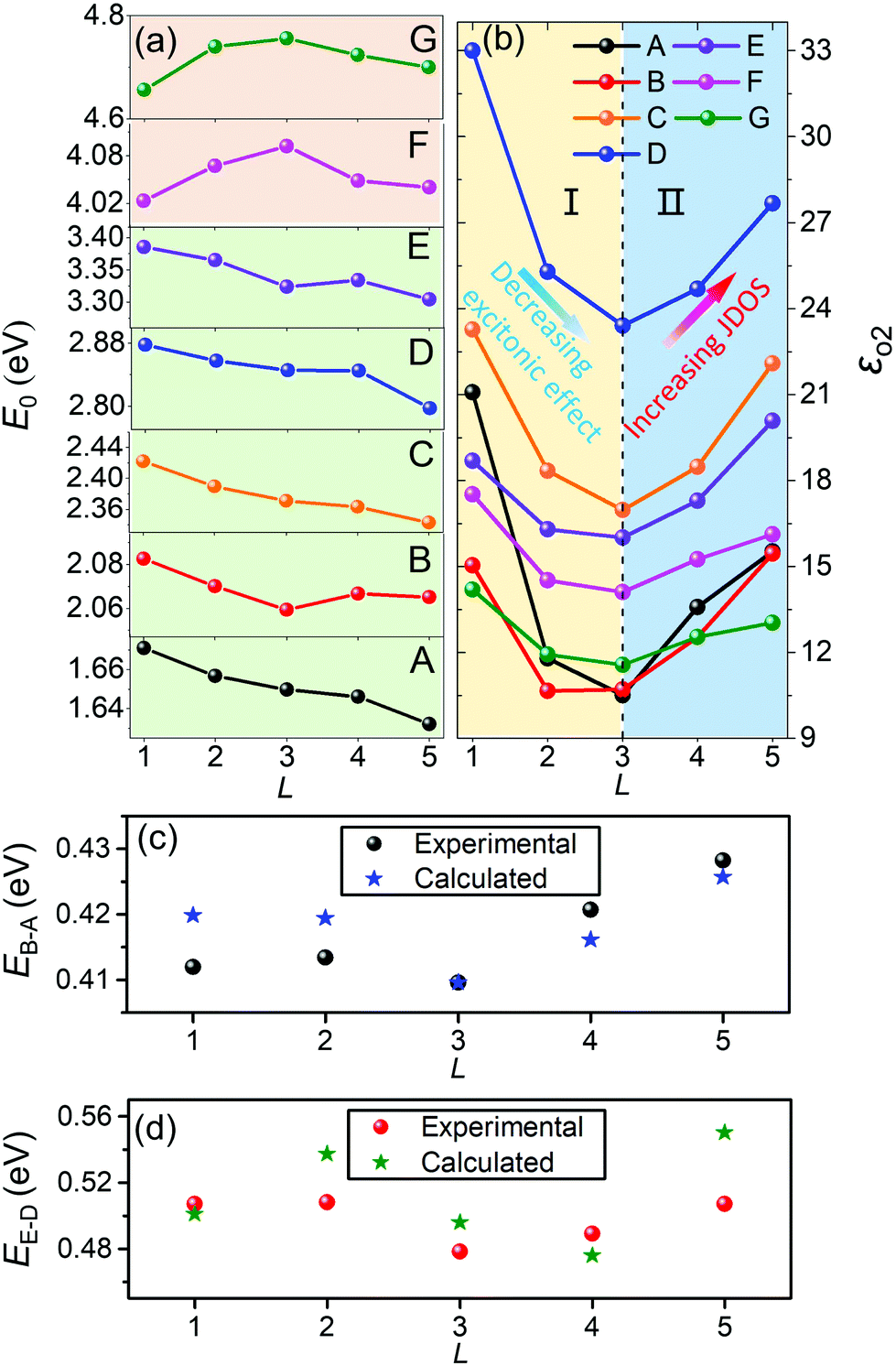 | ||
| Fig. 5 (a) Center energies of the critical points (CPs) A–G versus the layer number L. (b) The imaginary part εo2 of the in-plane dielectric function at these CPs versus L. (c and d) Energy splitting values between CPs B(E) and A(D) versus L. | ||
For CPs A–E, the second factor dominates their center energies when L ≤ 3, while the evolution of the center energies does not follow an apparent pattern as L changes from 3 to 5. In particular, for CPs A and C, the second factor still has a major influence on their center energies, while for the CPs B, D, and E, the competition between the above two factors gradually becomes significant. When L changes from 3 to 4, the sharply reduced exciton binding energies caused by the increasing out-of-plane dielectric shielding lead to a noteworthy blueshift of the center energies, whereas, as L goes up to 5, the prominent redshifts of the band-to-band absorption edge take back control of the center energies. For CPs F and G, the exciton effect in a high-energy range is expected to be more remarkable than that in the low-energy range, and the strongly decreasing exciton binding energies with the increase of L cause an obvious blueshift in the center energies when L ≤ 3. When L ≥ 3, the gradually enhanced interlayer interactions in multilayer WSe2 may further promote the shrinkage between CBs and VBs,14,54 which results in the redshifts in the center energies of CPs F and G. The redshift phenomenon also indicates that the electronic states associated with these transitions occurring at CPs F and G are extended in the out-of-plane direction.9
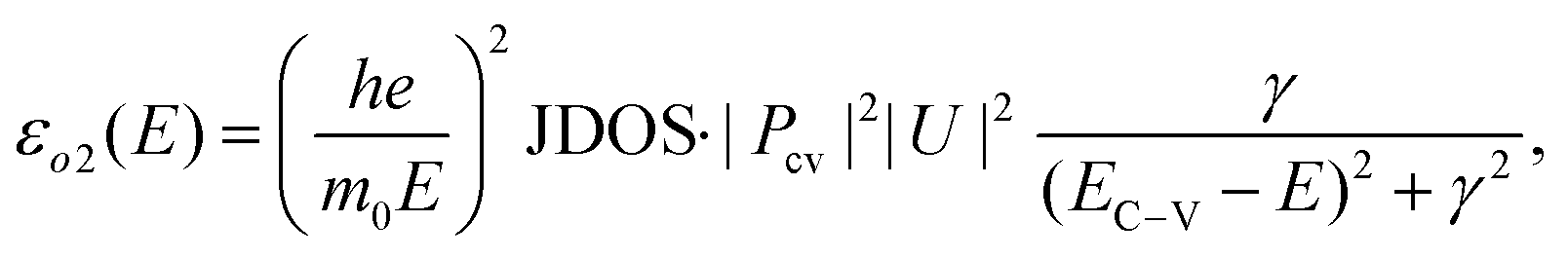
As illustrated in Fig. 5b, the imaginary parts of the in-plane dielectric function εo2 at above CPs demonstrate similar evolution patterns versus the layer number L. It can be seen that the εo2–L curves exhibit obvious valley shapes, whose bottom parts appear at L = 3. As shown in Fig. 5b, the εo2–L curves can be divided into two regions (region I and region II) based on the bottom parts. In region I, the magnitude of εo2 exhibits a layer-dependent decrease, while in region II, εo2 increases with the increasing layer number L. To figure out the physical mechanism behind the interesting layer-dependency that the dielectric function of 2D WSe2 exhibits, those parameters that have major influence on the dielectric function are investigated with the help of quantum mechanics. The imaginary part of the in-plane dielectric function εo2 is associated with the interband transitions and can be written as46,55
 | (2) |
Actually, for a thermal equilibrium system, the strength of the exciton effect can be represented by the exciton binding energy. To be specific, the exciton effect will be strong (weak) when the exciton binding energy is large (small). According to the above analysis of the exciton binding energy and some previous reports,51,52,56 we believe that the exciton effect decreases when WSe2 changes from a monolayer to the bulk limit. The JDOS means the density of paired initial–final states participating in the optical transition with a certain energy.46 Different from the layer-dependent decreasing exciton effect, the JDOS exhibits a monotonic layer-dependent increase. The acceleration of the JDOS gradually reduces and eventually approaches zero from a monolayer to the bulk.
In region I in Fig. 5b, with the increase of the layer number L, the rapidly decreasing exciton effect dominates the evolution trend for εo2 at these CPs, while, in region II, the uptrend of εo2 is mainly induced by the striking increase of the JDOS, and the weakened exciton effect also promotes this phenomenon. For WSe2, the change rates of the exciton effect and the JDOS reach a balance when L = 3, and the valley-like εo2–L curve appears at the bottom (Fig. 5b). Apparently, the layer-dependent changing rates (decreasing rates in region I and increasing rates in region II) of εo2 at different CPs are different from each other. This can be explained as a joint impact of two factors: (1) the out-of-plane dielectric shielding effect experienced by the exciton with a larger (smaller) Bohr radius is stronger (weaker), meaning that the strength of the exciton effect at different CPs shows dissimilar layer-dependencies; (2) the JDOSs at these CPs are different from each other (Fig. 5b), suggesting that the optical transition strength is different at these CPs. Furthermore, the steeper attenuation of εo2 for low-energy CPs A–D indicates that the exciton effects at these two CPs exhibit a stronger layer-dependency. For the remaining CPs, the relatively moderate decrease of εo2 arises from a collaborative influence of the weaker layer-sensibility of the exciton effect and the gradually significant offset from the increasing JDOS. Similar interpretations can be applied to comprehend the different increasing rates of εo2 presented in region II.
Fig. 5c and d present the experimental center energy differences between A(D) and B(E) compared with the theoretically calculated results (Fig. 4a and Fig. S5†). This phenomenon can be assigned to the energy band split induced by the SOC effect.57–59 The energy splitting values between CPs A and B (EB–A) for WSe2 specimens with different layers are 420 ± 10 meV (solid black balls, Fig. 5c), which agree well with the theoretical values 415 ± 10 meV (blue asterisks, Fig. 5c). It is obvious that EB–A values are nearly independent of the layer number L, especially for the monolayer and bilayer (L = 1, 2). The energy splitting values EB–A for the monolayer and bilayer are mainly induced by the intralayer SOC effect. The interlayer coupling only makes a weak contribution to enlarge the splitting slightly when L changes from 3 to 5. Similarly, the experimental and calculated energy splitting values between the CPs D and E (EE–D) (480 ± 40 meV for the experiment; 510 ± 50 meV for the calculation) are relatively consistent with each other (Fig. 5d). It can be found that the EE–D data undergo a similar changing rule to EB–A, which is because CPs E and D are caused by the SOC-induced band nesting phenomenon.49
4. Conclusions
In summary, we firstly prepared high-quality, continuous, and centimeter-scale 2D WSe2 with different layers on sapphire by an ultrafast ambient-pressure chemical vapor deposition method. Then, the evolution of layer-dependent dielectric and optical properties of 2D WSe2 from a single layer to 5 layers was comprehensively investigated by broadband (0.73–6.42 eV) spectroscopic ellipsometry. We propose a systematic method based on the CP analysis and first-principles calculations to identify the spatial positions in the BZ, energy bands, and carrier types of the optical transitions occurring at the CPs of 2D WSe2. Dielectric functions and the complex refractive indices of 1–5L WSe2 are determined from the measured ellipsometric parameters, and up to eight CPs (A–H) are distinguished in the in-plane dielectric function spectra. Specific transitions responsible for these CPs are further precisely identified by using the proposed method. Results demonstrate that the layer-dependent evolution of the center energies of these CPs occurs according to two different rules. For the five low-energy CPs (A–E), their center energies exhibit general redshift tendencies as the layer number increases, while the center energies of the high-energy CPs (F and G) firstly present a blueshift (L ≤ 3) and then a redshift (L ≥ 3). The underlying physical cause of the distinctive layer-dependency is explained as the alternate domination of the layer-dependent decreasing exciton binding energy and the band renormalization. We find that the imaginary part of the in-plane dielectric functions presents a valley shape versus the layer number of the WSe2, and the valley bottom appears at 3L. This layer-dependent fluctuation can be attributed to the joint contribution from the decreasing exciton effect and the increasing JDOS. In addition, the layer-dependent energy band split induced by the SOC effect is studied, and the experimental energy splitting values between CPs A(D) and B(E) show high agreement with the theoretical results. These layer-dependent dielectric and optical properties of 2D WSe2 revealed in this work are promising in advancing the fundamental understanding of the electronic structures, which is helpful for the optimal design and performance improvement of related devices.Conflicts of interest
There are no conflicts to declare.Acknowledgements
This work was funded by the National Natural Science Foundation of China (Grant No. 51727809, 51525502, 51805193, and 51775217), the China Postdoctoral Science Foundation (Grant No. 2016M602288 and 2017T100546), the National Science and Technology Major Project of China (Grant No. 2017ZX02101006-004), and the National Science Foundation of Hubei Province of China (Grant No. 2018CFB559 and 2018CFA057). The authors are thankful for the technical support from the Experiment Center for Advanced Manufacturing and Technology in School of Mechanical Science & Engineering of HUST.Notes and references
- Y. Zhang, M. M. Ugeda, C. H. Jin, S.-F. Shi, J. B. Aaron, A. Martín-Recio, H. Ryu, J. Kim, S. Tang, Y. Kim, B. Zhou, C. Hwang, Y. Chen, F. Wang, M. F. Crommie, Z. Hussain, Z.-X. Shen and S.-K. Mo, Nano Lett., 2016, 16, 2485–2491 CrossRef CAS PubMed.
- Z. Wu, Z. Luo, Y. Shen, W. Zhao, W. Wang, H. Nan, X. Guo, L. Sun, X. Wang, Y. You and Z. Ni, Nano Res., 2016, 9, 3622–3631 CrossRef CAS.
- H. Zhou, C. Wang, J. C. Shaw, R. Cheng, Y. Chen, X. Huang, Y. Liu, N. O. Weiss, Z. Lin, Y. Huang and X. Duan, Nano Lett., 2015, 15, 709–713 CrossRef CAS PubMed.
- T. Y. Kim, A. Ferretti and C.-H. Park, Phys. Rev. B, 2018, 98, 245410 CrossRef CAS.
- D.-Y. Lin, J.-J. Jheng, T.-S. Ko, H.-P. Hsu and C.-F. Lin, AIP Adv., 2018, 8, 055011 CrossRef.
- C. Jin, J. Kim, M. I. B. Utama, E. C. Regan, H. Kleemann, H. Cai, Y. Shen, M. J. Shinner, A. Sengupta, K. Watanabe, T. Taniguchi, S. Tongay, A. Zettl and F. Wang, Science, 2018, 360, 893–896 CrossRef CAS PubMed.
- C. Zhou, S. Raju, B. Li, M. Chan, Y. Chai and C. Y. Yang, Adv. Funct. Mater., 2018, 28, 1802954 CrossRef.
- P. Lin, L. Zhu, D. Li, L. Xu, C. Pan and Z. Wang, Adv. Funct. Mater., 2018, 28, 1802849 CrossRef.
- W. Zhao, Z. Ghorannevis, L. Chu, M. Toh, C. Kloc, P.-H. Tan and G. Eda, ACS Nano, 2013, 7, 791–797 CrossRef CAS.
- Y. Niu, S. Gonzalez-Abad, R. Frisenda, P. Marauhn, M. Drüppel, P. Gant, R. Schmidt, N. S. Taghavi, D. Barcons, A. J. Molina-Mendoza, S. M. D. Vasconcellos, R. Bratschitsch, D. P. D. Lara, M. Rohlfing and A. Castellanos-Gomez, Nanomaterials, 2018, 8, 725 CrossRef PubMed.
- X.-L. Li, W.-P. Han, J.-B. Wu, X.-F. Qiao, J. Zhang and P.-H. Tan, Adv. Funct. Mater., 2017, 27, 1604468 CrossRef.
- M. Zhu, K. Huang and K.-G. Zhou, Prog. Cryst. Growth Charact. Mater., 2017, 63, 72–93 CrossRef CAS.
- W. Shi, M.-L. Lin, Q.-H. Tan, X.-F. Qiao, J. Zhang and P.-H. Tan, 2D Mater., 2016, 3, 025016 CrossRef.
- E. D. Corro, H. Terrones, A. Elias, C. Fantini, S. Feng, M. A. Nguyen, T. E. Mallouk, M. Errones and M. A. Menta, ACS Nano, 2014, 8, 9629–9635 CrossRef PubMed.
- Y. Li, A. Chernikov, X. Zhang, A. Rigosi, H. M. Hill, A. M. Zande, D. A. Chenet, E.-M. Shih, J. Hone and T. F. Heinz, Phys. Rev. B: Condens. Matter Mater. Phys., 2014, 90, 205422 CrossRef.
- Y. V. Morozov and M. Kuno, Appl. Phys. Lett., 2015, 107, 083103 CrossRef.
- A. A. Govyadinov, S. Mastel, F. Golmar, A. Chuvilin, P. S. Carney and R. Hillenbrand, ACS Nano, 2014, 8, 6911–6921 CrossRef CAS PubMed.
- D. Hu, X. Yang, C. Li, R. Liu, Z. Yao, H. Hu, S. N. G. Corder, J. Chen, Z. Sun, M. Liu and Q. Dai, Nat. Commun., 2017, 8, 1471 CrossRef PubMed.
- D. Wintz, K. Chaudhary, K. Wang, L. A. Jauregui, A. Ambrosio, M. Tamagnone, A. Y. Zhu, R. C. Devlin, J. D. Crossno, K. Pistunova, K. Watanabe, T. Taniguchi, P. Kim and F. Capasso, ACS Photonics, 2018, 5, 1196–1201 CrossRef CAS.
- X. Chen, D. Hu, R. Mescall, G. You, D. N. Basov, Q. Dai and M. Liu, Adv. Mater., 2019, 31, 1804774 CrossRef PubMed.
- S. M. Eichfeld, C. M. Eichfeld, Y.-C. Lin, H. Lorraine and A. R. Joshua, APL Mater., 2014, 2, 092508 CrossRef.
- V. G. Kravets, V. V. Prorok, L. V. Poperenko and I. A. Shaykevich, Semicond. Phys., Quantum Electron. Optoelectron., 2017, 20, 284–296 CrossRef CAS.
- M. S. Diware, K. Park, J. Mun, H. G. Park, W. Chegal, Y. J. Cho, H. M. Cho, J. Park, H. Kim, S.-W. Kang and Y. D. Kim, Curr. Appl. Phys., 2017, 17, 1329–1334 CrossRef.
- M. S. Diware, S. P. Ganorkar, K. Park, W. Chegal, H. M. Cho, Y. J. Cho, Y. D. Kim and H. Kim, J. Phys.: Condens. Matter, 2018, 30, 235701 CrossRef CAS PubMed.
- B. Song, H. Gu, S. Zhu, H. Jiang, X. Chen, C. Zhang and S. Liu, Appl. Surf. Sci., 2018, 439, 1079–1087 CrossRef CAS.
- S. Liu, X. Chen and C. Zhang, Thin Solid Films, 2015, 584, 176–185 CrossRef CAS.
- P. Johari and V. B. Shenoy, ACS Nano, 2011, 5, 5903–5908 CrossRef CAS PubMed.
- A. Kumar and P. K. Ahluwalia, Phys. B, 2012, 407, 4627–4634 CrossRef CAS.
- Y. Gao, Y.-L. Hong, L.-C. Yin, Z. Wu, Z. Yang, M.-L. Chen, Z. Liu, T. Ma, D.-M. Sun, Z. Ni, X.-L. Ma, H.-M. Chen and W. Ren, Adv. Mater., 2017, 29, 1700990 CrossRef PubMed.
- Y. Gao, Z. Liu, D.-M. Sun, L. Huang, L.-P. Ma, L.-C. Yin, T. Ma, Z. Zhang, X.-L. Ma, L.-M. Peng, H.-M. Cheng and W. Ren, Nat. Commun., 2015, 6, 8569 CrossRef CAS PubMed.
- B. Song, H. Gu, M. Fang, X. Chen, H. Jiang, R. Wang, T. Zhai, Y.-T. Ho and S. Liu, Adv. Opt. Mater., 2018, 7, 180125 Search PubMed.
- H. Gu, X. Chen, H. Jiang, C. Zhang and S. Liu, J. Opt., 2016, 18, 025702 CrossRef.
- G. Kresse and J. Furthmüller, Phys. Rev. B: Condens. Matter Mater. Phys., 1996, 54, 11169–11186 CrossRef CAS PubMed.
- J. P. Perdew, K. Burke and M. Ernzerhof, Phys. Rev. Lett., 1996, 77, 3865 CrossRef CAS PubMed.
- A. V. Krukau, O. A. Vydrov, A. F. Izmaylov and G. E. Scuseria, J. Chem. Phys., 2006, 125, 224106 CrossRef PubMed.
- S. Seo, H. Choi, S.-Y. Kim, J. Lee, K. Kim, S. Yoon, B. H. Lee and S. Lee, Adv. Mater. Interfaces, 2018, 5, 1800524 CrossRef.
- X. Zhang, X.-F. Qiao, W. Shi, J.-B. Wu, D.-S. Jiang and P.-H. Tan, Chem. Soc. Rev., 2015, 44, 2757 RSC.
- H. Fujiwara, Spectroscopic Ellipsometry: Principles and Applications, John Wiley & Sons, Chichester, West Sussex, England, 2007 Search PubMed.
- D. E. Aspnes, J. B. Theeten and F. Hottier, Phys. Rev. B: Condens. Matter Mater. Phys., 1979, 20, 3292–3302 CrossRef CAS.
- A. Yanguas-Gil and H. Wormeester, Ellipsometry at the Nanoscale, ed. M. Losurdo and K. Hingerl, Springer, Berlin, Heidelberg, Germany, 2013, pp. 179–202 Search PubMed.
- S. Funke, B. Miller, E. Parzinger, P. Thiesen, A. W. Holleitner and U. Wurstbauer, J. Phys.: Condens. Matter, 2016, 28, 385301 CrossRef CAS PubMed.
- A. S. Ferlauto, G. M. Ferreira, J. M. Pearce, C. R. Wronski, R. W. Collins, X. Deng and G. Ganguly, J. Appl. Phys., 2002, 92, 2424–2436 CrossRef CAS.
- I. Malitson and M. Dodge, J. Opt. Soc. Am., 1972, 62, 1405 Search PubMed.
- H. G. Tompkins and E. A. Irene, Handbook of Ellipsometry, William Andrew, Norwich, NY, 2005 Search PubMed.
- A. C. Diebold, F. J. Nelson and V. K. Kamineni, in Ellipsometry at the Nanoscale, ed. M. Losurdo and K. Hingerl, Springer, Berlin, Heidelberg, Germany, 2013, pp. 557–581 Search PubMed.
- P. Y. Yu and M. Cardona, Fundamentals of Semiconductors Physics and Materials Properties, Springer, Berlin, Heidelberg, Germany, 2010 Search PubMed.
- X. Fan, D. J. Singh and W. Zheng, J. Phys. Chem. Lett., 2016, 7, 2175–2181 CrossRef CAS PubMed.
- D. W. Latzke, W. Zhang, A. Suslu, T.-R. Chang, H. Lin, H.-T. Jeng, S. Tongay, J. Wu, A. Bansil and A. Lanzara, Phys. Rev. B: Condens. Matter Mater. Phys., 2015, 91, 235202 CrossRef.
- A. Carvalho, R. M. Ribeiro and A. H. C. Neto, Phys. Rev. B: Condens. Matter Mater. Phys., 2013, 88, 115205 CrossRef.
- R. Schmidt, I. Niehues, R. Schneider, M. Drüppel, T. Deilmann, M. Rohlfing, S. M. D. Vasconcellos, A. Castellanos-Gomez and R. Bratschitsch, 2D Mater., 2016, 3, 021011 CrossRef.
- A. Chernikov, T. C. Berkelbach, H. M. Hill, A. Rigosi, Y. Li, O. B. Aslan, D. R. Reichman, M. S. Hybertsen and T. F. Heinz, Phys. Rev. Lett., 2014, 113, 076802 CrossRef PubMed.
- T. Olsen, S. Latini, F. Rasmussen and K. S. Thygesen, Phys. Rev. Lett., 2016, 116, 056401 CrossRef PubMed.
- T. C. Berkelbach, M. S. Hybertsen and D. R. Reichman, Phys. Rev. B: Condens. Matter Mater. Phys., 2013, 88, 045318 CrossRef.
- M. Koperski, M. R. Molas, A. Arora, K. Nogajewski, A. O. Slobodeniuk, C. Faugeras and M. Potemski, Nanophotonics, 2017, 6, 1289–1308 CAS.
- D. A. B. Miller, J. S. Weiner and D. S. Chemla, IEEE J. Quantum Electron., 1986, 22, 1816–1830 CrossRef.
- Y. Lin, X. Ling, L. Yu, S. Huang, A. L. Hsu, Y.-H. Lee, J. Kong, M. S. Dresselhaus and T. Palacios, Nano Lett., 2014, 14, 5569–5576 CrossRef CAS PubMed.
- A. Ramasubramaniam, Phys. Rev. B: Condens. Matter Mater. Phys., 2012, 86, 115409 CrossRef.
- W.-T. Hsu, L.-S. Lu, D. Wang, J.-K. Huang, M.-Y. Li, T.-R. Chang, Y.-C. Chou, Z.-Y. Juang, H.-T. Jeng, L.-J. Li and W.-H. Chang, Nat. Commun., 2017, 8, 929 CrossRef PubMed.
- K. F. Mak, C. Lee, J. Hone, J. Shan and T. F. Heinz, Phys. Rev. Lett., 2010, 105, 136805 CrossRef PubMed.
Footnotes |
| † Electronic supplementary information (ESI) available. See DOI: 10.1039/c9nr04270a |
| ‡ These authors contributed equally to this work. |
| This journal is © The Royal Society of Chemistry 2019 |