
 Open Access Article
 This Open Access Article is licensed under a
 Creative Commons Attribution 3.0 Unported Licence
Growth modes and quantum confinement in ultrathin vapour-deposited MAPbI3 films†
Elizabeth S.
Parrott
 a,
Jay B.
Patel
a,
Amir-Abbas
Haghighirad
b,
Henry J.
Snaith
a,
Michael B.
Johnston
a and
Laura M.
Herz
*a
a,
Jay B.
Patel
a,
Amir-Abbas
Haghighirad
b,
Henry J.
Snaith
a,
Michael B.
Johnston
a and
Laura M.
Herz
*a
aDepartment of Physics, University of Oxford, Clarendon Laboratory, Parks Road, Oxford OX1 3PU, UK. E-mail: laura.herz@physics.ox.ac.uk
bKarlsruhe Institute of Technology, 76021 Karlsruhe, Germany
First published on 12th July 2019
Abstract
Vapour deposition of metal halide perovskite by co-evaporation of precursors has the potential to achieve large-area high-efficiency solar cells on an industrial scale, yet little is known about the growth of metal halide perovskites by this method at the current time. Here, we report the fabrication of MAPbI3 films with average thicknesses from 2–320 nm by co-evaporation. We analyze the film properties using X-ray diffraction, optical absorption and photoluminescence (PL) to provide insights into the nucleation and growth of MAPbI3 films on quartz substrates. We find that the perovskite initially forms crystallite islands of around 8 nm in height, which may be the cause of the persistent small grain sizes reported for evaporated metal halide perovskites that hinder device efficiency and stability. As more material is added, islands coalesce until full coverage of the substrate is reached at around 10 nm average thickness. We also find that quantum confinement induces substantial shifts to the PL wavelength when the average thickness is below 40 nm, offering dual-source vapour deposition as an alternative method of fabricating nanoscale structures for LEDs and other devices.
Introduction
Metal halide perovskites with the formula ABX3, (where A is a cation such as cesium or methylammonium, B is usually lead, and X is a halide) have attracted much interest due to their ease of fabrication,1 widely tunable direct optical band gap,2–5 and exceptional electronic properties.6,7 They have been successfully employed in solar cells,8–11 resulting in certified power conversion efficiencies (PCE) over 22%,10 and have also proved effective in other optoelectronic devices such as light emitting diodes (LEDs)12–14 and lasers.15,16 One advantage of these materials is that they can be fabricated by a variety of methods1 including spin coating, a method which enables quick and easy fabrication of small scale samples in the laboratory. Whilst the widespread use of this technique has facilitated rapid advances in the technology, the development of techniques which can reliably reproduce high-quality films at large scale has lagged behind. This must be addressed if perovskites are to be scaled up for commercial use and reach their full potential in large scale renewable energy generation.1Vapour deposition by thermal evaporation, is a technique suitable for large scale device fabrication17 and produces uniform, smooth thin films8 with precise control over the film thickness.18 These qualities have proved successful in fabricating a range of metal halide perovskite materials for solar cells,8,17,19,20 flexible devices,21 and amplified spontaneous emission.16 It also enables uniform coating of rough surfaces such as pyramid-textured silicon for use in efficient perovskite-silicon tandem solar cells.22 Fabricating metal halide perovskites by this method involves evaporation of solid precursors of type AX and BX2 (such as CH3NH3I and PbI2) by two possible methods; a sequential deposition method and a co-evaporation method. For the sequential deposition method,23 the precursors are evaporated in separate layers, which diffuse into each other to form the perovskite. However this method has yielded a maximum PV device PCE of only 16% to date,24 and requires annealing, which can introduce thermal strain.25,26 A more successful method is the co-evaporation technique in which the precursors are simultaneously evaporated from two sources to form the perovskite directly on the substrate.27 This method ensures the composition is the same throughout the film with no additional annealing, and has been used to make devices with a PCE of 20.3%.28
One factor responsible for the leap in both the efficiency and stability of solution processed devices was the control of film morphology by engineering the growth process.29,30 This has led to vastly enlarged grain sizes reaching the millimeter scale,31 a development which has been linked to improved solar cell performance7,12,32 and enhanced stability.33,34 In contrast, thermally evaporated films still show very limited grain size on the order of 100 nm.8,18,21,27,35 Although relatively high efficiency devices can still be fabricated even at this suboptimal grain size, their stability remains to be optimised.28,36 Resolving the problem of small grain sizes by understanding the early stages of film growth is therefore paramount to improvement.
An additional advantage of understanding the growth of MAPbI3 thin films is its application to growing nanostructures for use in LEDs and other electronic devices. Metal halide perovskites have been used to make LEDs in many different architectures.14,37–41 Nanocrystals and 2D perovskites are particularly attractive for this purpose since the charge-carriers exhibit quantum confinement, which boosts the radiative recombination rate, narrows the emission linewidth, and allows for wavelength tunability by controlling the size of the crystals or the thickness of quasi-2D layers.37,42 Nanocrystals can exhibit PL quantum efficiency of over 90% in solution, yet in devices it is challenging to produce an external quantum efficiency (EQE) of over 6% due to ligands preventing good charge transport.37 2D perovskites have been employed in a multi-quantum-well type structure,14 but since the thickness and arrangement of the layers cannot be fully controlled41 this also hinders charge transport.39 Recent breakthroughs have seen a handful of devices achieving EQE as high as 20% (ref. 38–40) but there is still room for improvement. In traditional inorganic semiconductors, confinement has been achieved by growing quantum wells by controlled deposition methods with EQE of over 80%.43 Perovskite quantum well structures for LEDs have been attempted via solution processing, with pinhole free layers as thin as 35 nm achieved.44 However, the observation of quantum confinement will require even thinner layers, and although a layer with nominal thickness down to 15 nm has been implemented in a device, non-uniformities hampered the efficiency.45 Vapour deposition can yield higher uniformity, but so far, LEDs based on this approach have been implemented with layer thicknesses between 50 and 300 nm.46,47 Reducing thermally evaporated hybrid perovskite layers to dimensions thin enough for quantum confinement could combine the benefits of electronic confinement and good charge transport. If perovskite layers could be reliably grown by thermal evaporation at dimensions thin enough for quantum confinement, this could combine the benefits of confinement and good charge transport. Understanding the formation of metal halide perovskite thin films could therefore provide alternative methods for fabricating efficient LEDs.
Characterization of the early stages of thin film development can be challenging, since it requires analysis of a very small amount of material. Metal halide perovskites are soft materials and prone to degradation, which makes the use of imaging techniques challenging. For example, transmission electron microscopy (TEM) can be used to directly image the morphology of a very thin film, but requires the film to be exposed to a high energy electron beam, under which MAPbI3 is liable to degrade.48 Even atomic force microscopy (AFM) can cause changes to the film due to the interaction of the tip and the surface.32 Other characterization methods can be undertaken in situ, using bespoke deposition chambers to take measurements in real time, or ex situ, by growing films of increasing thickness under the same conditions. In situ X-ray diffraction (XRD) measurements have been carried out during co-evaporation of several metal halide perovskites,49,50 however the time resolution is limited by the amplitude of the signal, and so these measurements were not able to capture the early stages of growth where the signal is low. Ex situ XRD51 and XPS51–53 measurements on MAPbI3 show the formation of additional species at the perovskite-substrate interface such as PbI2![[thin space (1/6-em)]](https://www.rsc.org/images/entities/char_2009.gif) 51,53 and decomposition products of MAI,52 which prevents the growth of pure MAPbI3 thin films.
51,53 and decomposition products of MAI,52 which prevents the growth of pure MAPbI3 thin films.
In this letter, we report the growth of thin films of MAPbI3 with average thickness as small as 2 nm with no detectable presence of PbI2 in the XRD spectrum. By comparing optical absorption and XRD measurements we find evidence for a Volmer–Weber type growth mode (island growth), with material in the thinnest films coalescing into crystallites with a height of around 7–8 nm, small enough to display significant PL blue-shift due to quantum confinement, which offers a simple alternative route to fabricating nanocrystals. Substrate coverage is achieved at a thickness of 10 nm which is promising for growing quantum well structures. Even without confinement, it has been shown that reducing the thickness of the perovskite in LEDs increases the efficiency.44 By further optimization of the deposition process and material–substrate interaction to encourage layer-by-layer deposition, there is the potential for even thinner films to be formed. Achieving layer-by-layer deposition could also be beneficial towards increasing the grain size in thicker films which could help improve the efficiency and stability of solar cells, since the island growth mode may be responsible for the limited grain size.
Results and discussion
To investigate different stages of growth, we first evaporated 7 batches of MAPbI3 films at different thicknesses by changing the length of time for which the substrate was exposed to MAI and PbI2 vapour in the evaporator. We observed a visible color difference from almost transparent brown to opaque black as the thickness was increased (Fig. 1 inset). We determined the thickness by matching the optical absorption between 550 nm and 700 nm to the absorption coefficient previously determined for identically fabricated MAPbI3 in this wavelength range18 (see ESI and Fig. S3† for full details). From here on we will refer to the average physical thickness of a MAPbI3 film determined by this method as the ‘optical thickness’. The determined optical thicknesses are shown in Fig. 1 for each evaporation time. The linear fit shows that the deposition occurred approximately linearly at a rate of 0.085 nm s−1.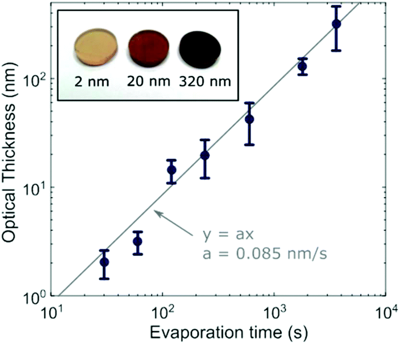 | ||
| Fig. 1 Thickness calculated by matching the absorbance of each sample to a known absorption coefficient in the range 550–700 nm (optical thickness). The grey line is the fit (y = ax) to the data, giving a deposition rate of 0.085 nm s−1. The inset is a photograph of the 2, 20 and 320 nm MAPbI3 films on 2 mm-thick quartz substrates, showing that the difference in absorption can be seen by eye. | ||
We characterized the films using X-ray diffraction (XRD), with the angles referenced to the quartz reflection (marked with an asterisk in Fig. 2a) to account for any small offset in the angle of the sample. All samples showed peaks at the expected angles for (100) and (200) crystallographic planes, with the thickest samples showing several additional peaks of lower intensity originating from other crystallographic orientations. These orientations may be present in all samples, but the corresponding peaks would be indistinguishable in the thinner films due to the lower signal to noise ratio (Fig. S4†). The (100) and (200) peaks of the thinner films showed slight angular shifts in comparison to the thickest film, corresponding to a global expansion of the lattice parameter. In the XRD geometry for our experiment the lattice planes contributing to the peaks are in the plane of the substrate, so the measured expansion corresponds to tensile strain perpendicular to the substrate. The cause could either be volume expansion or, more likely, compressive biaxial strain in the plane of the substrate which induces an out-of-plane expansion26 (since the Poisson ratio has been theoretically predicted to be 0.33).54 Since the pseudo-cubic lattice parameter of 6.275 Å measured for the thickest sample falls within the range of previously measured values for unstrained MAPbI3,55–57 we calculate strain relative to this value and plot the result in Fig. 2b. As the film grows, strain increases up to a maximum, then decreases and becomes small above 50 nm.
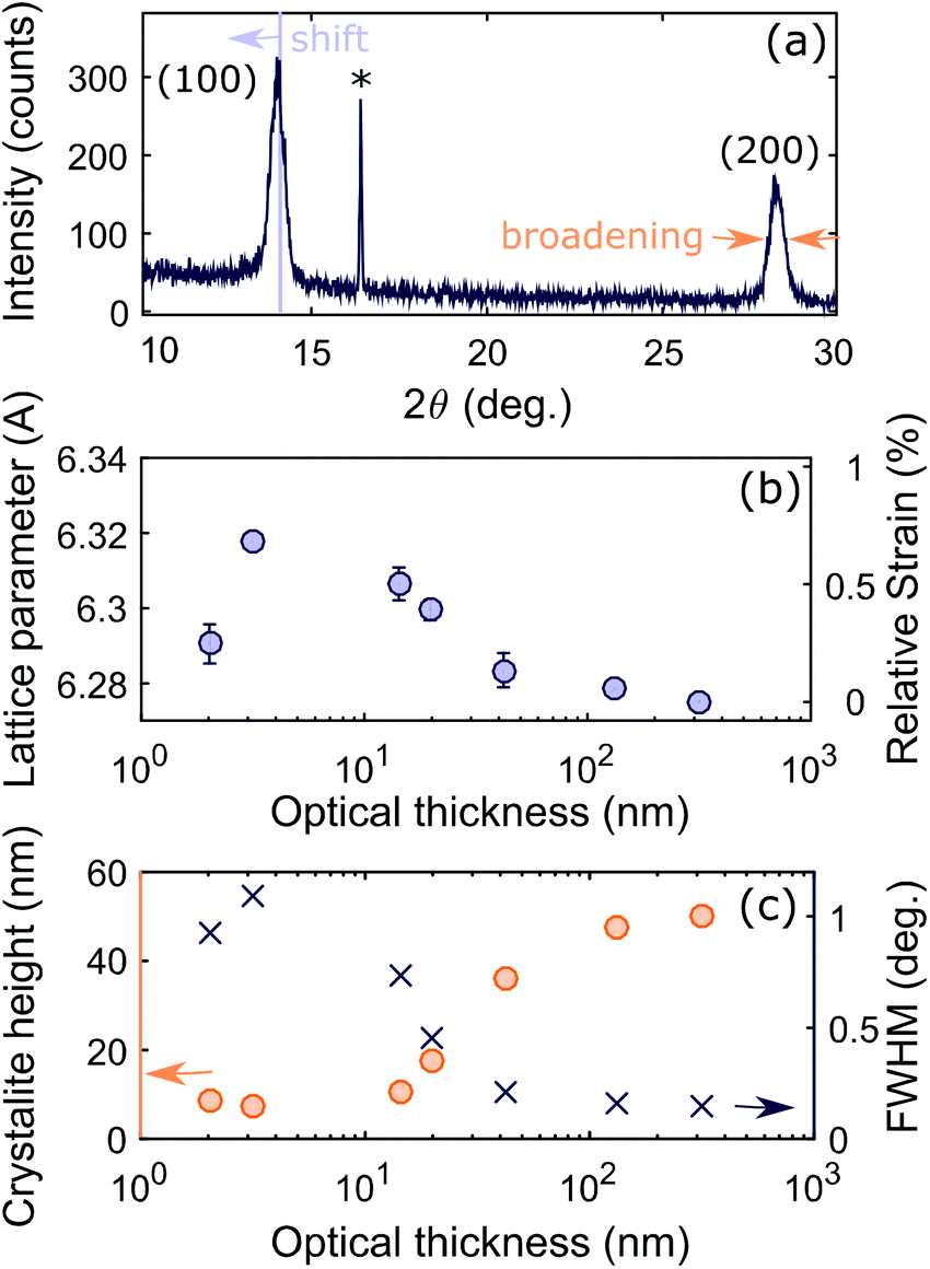 | ||
| Fig. 2 (a) Example of XRD data for 42 nm sample shown to illustrate the peak shift from which the strain is determined and the broadening from which the crystallite height is determined. Full XRD spectra are shown in Fig. S4.† (b) The lattice parameter (in Angstrom) is the mean of the lattice parameter for the (100) and (200) peaks. The error bar indicates the difference between the two values. The strain is calculated relative to that of the thickest sample. (c) The crystallite height (orange circles) is calculated from the full width at half maximum of the peak (blue crosses) using the Scherrer equation (see ESI†). | ||
There are three main causes of strain in polycrystalline thin films: (i) misfit strain, which occurs when a film grows epitaxially on a substrate with a mismatch between the substrate and film lattice parameters; (ii) thermal strain, which occurs due to a temperature change when there is a difference between the thermal expansion coefficients of the substrate and film; and (iii) intrinsic strain, which is affected by the growth conditions and includes factors such as the energy minimization of crystal surfaces and the effect of impurities.58 Coherent strain is ruled out since the mismatch between the perovskite and the relevant lattice parameter of the z-cut quartz substrate (4.9 Å) is too large for epitaxial growth. Thermal strain occurs in annealed perovskite films due to the large thermal expansion coefficient and results in the out-of-plane lattice parameter shrinking,25,26 which is a change in the opposite direction to our measurements. Thermal strain is unlikely to occur here since the substrate was held at room temperature throughout the deposition, storage and measurements. The strain we observe is therefore most likely to be intrinsic.
Intrinsic strain has been observed in metal halide perovskites made by solution methods due to intermediate complexes in the crystallization process.25 This cannot be the mechanism here since no solvents are used in thermal evaporation. Changes in intrinsic strain as growth progresses are commonly seen in inorganic crystalline thin films fabricated by vapour deposition methods.58,59 For island growth, surface energy minimization of the exposed crystal faces and material–substrate interface generates strain, usually compressive strain in the plane of the substrate.60 As more material is deposited and the edges of the islands approach each other, the gap decreases until cohesion causes the material to elastically stretch and coalesce.61 For a fully covered substrate, the surface stresses are no longer as important since there is less surface area, and the lattice parameter tends to its bulk value. This could be the mechanism driving the initial rise in strain followed by relaxation, which we observe with increasing film thickness. Alternatively the strain may be induced by impurities originating from the evaporation source or from degradation products. Others have seen either an excess of PbI2 at the substrate interface due to the superior wetability of PbI2 in comparison to MAI,51 or a presence of MAI degradation products due to a catalytic interaction with the substrate.52 We do not see any evidence of PbI2 in the XRD spectra and we believe the quartz substrates used are unlikely to cause decomposition of MAI. Shifts in the Raman spectra of MAPbI3 nanoplatelets grown by chemical vapour deposition have been observed at similar thicknesses, which the authors attributed to lattice distortion at the interface, a theory which may be supported by the increased strain we observe.62
Next, we determine the height of the crystallites in the perovskite film from the XRD spectra by measuring the line broadening that occurs due to the finite number of lattice planes limiting the X-ray coherence length. More broadening therefore implies that the crystallite is smaller in the direction perpendicular to the substrate. We determined the full width at half maximum (FWHM) of the (100) perovskite peak by fitting a pseudo-Voigt function, and corrected this value for instrument broadening by comparison to the FWHM of the XRD peaks of a silicon reference (see ESI† for full details). We then determined the crystallite height from the FWHM using the Scherrer equation (equation (S5)†).63 The FWHM and crystallite height are shown in Fig. 2c.
This analysis neglects any contribution to broadening of the XRD peaks from microstrain, which is a measure of the distribution of lattice parameters present in the material due to inhomogeneity. The Scherrer equation is valid for thinner films where size broadening dominates over microstrain, and is therefore often used to determine the size of nanocrystals.42,64 However, the values for crystallite size determined by this method become inaccurate as the film thickness increases, and should be seen instead as a lower limit on the crystallite size. To achieve a more accurate value of the crystallite height, the contributions from microstrain and size broadening can be separated by determining the FWHM of multiple XRD peaks and employing the Williamson–Hall plot method.65 We have undertaken this analysis for the thickest film (optical thickness of 320 nm) for which enough peaks are distinguishable in the XRD spectrum to accurately separate the two contributions, with the resulting plot shown in Fig. S6.† The analysis yields a crystallite height of 75 nm and a microstrain of 0.16%, from which we conclude that the microstrain is small, and that its inclusion provides only a minor correction to the values of crystallite height obtained from the Scherrer equation alone. The value of microstrain determined here is lower than the value of 0.65% which has been previously derived by the same method for MAPbI3 fabricated by solution processing.66 If these values are intrinsic to the growth conditions, lower microstrain could be an additional benefit of fabricating MAPbI3 by co-evaporation, since microstrain has been linked to poorer device performance67 and higher risk of mechanical failure due to delamination.68
By plotting the ratio (r) of the crystallite height to the optical thickness, as shown in Fig. 3, we can deduce three stages in the film growth of MAPbI3 on quartz by thermal evaporation. An illustration of the crystallite height and optical thickness in the first and third stage of growth can be found in Fig. S9.† In the first stage when the optical thickness is below 10 nm, the material is formed in single crystallite islands, around 7 nm in height. The ratio r remains below 1, since the height of the islands is larger than the average film thickness (optical thickness). Increasing the evaporation time increases the proportion of the film covered by islands, and therefore the optical thickness, but there is no change in the height of the islands at this initial stage of the growth process. In the second stage, full coverage is reached and the crystallites begin to grow upwards with the ratio r equal to one. In the third stage, the crystallite height plateaus but the film thickness continues to increase. Since the crystallite height is a measure of the number of coherent lattice planes, a crystallite height smaller than the optical thickness means there are multiple crystal orientations stacked on top of each other within the thin film. The ratio r is therefore greater than one, though the values here are slightly exaggerated by neglecting the effect of microstrain in our crystallite height determination, as discussed above. The three stages of growth outlined above also correspond to the build-up, release, and plateau of strain respectively, consistent with our suggestion of intrinsic strain being caused by island growth.
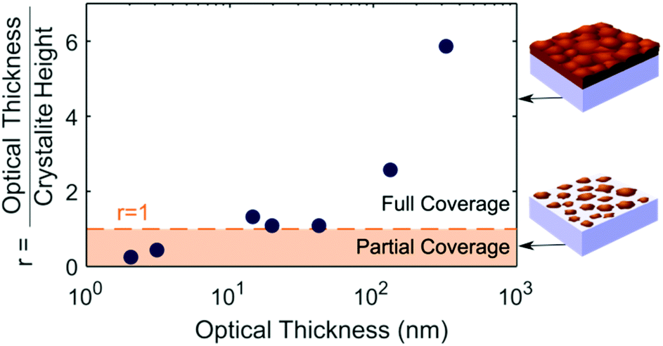 | ||
| Fig. 3 Ratio of the thickness determined from the absorption coefficient (optical thickness), and the grain height calculated from XRD FWHM. When the ratio is equal to one or more, the surface of the substrate is fully covered, as illustrated. | ||
Thin films display three primary growth modes – island (Volmer–Weber), layer-by-layer (Frank–van der Merwe) and layer-plus-island (Stranski–Krastanov). Stranski–Krastanov growth requires that the substrate has a similar lattice parameter to the deposition material, allowing the initial formation of epitaxial layers up to a critical thickness followed by island formation to release strain caused by lattice misfit between the substrate and deposition material.69 Island and layer-by-layer growth modes are not limited to materials grown on lattice matched substrates, and can occur in non-epitaxial film growth where the initial nucleation largely depends on the minimization of surface energy. Volmer–Weber type growth typically occurs when the cohesion energy (between the material and itself) is larger than the adhesion energy (between substrate and material).70 It is therefore energetically favorable for the material to cluster, rather than forming a uniform layer on the substrate. Frank–van der Merwe type growth occurs under the opposite condition, when the adhesion energy is larger than the cohesion energy.70 The Volmer–Weber type island growth mode we observe here could explain why the grain size of vapour deposited perovskites is small (around 100 nm) compared to solution deposited thin films, since the lateral grain size is determined by the initial nucleation of the crystals. A detailed study investigating different growth parameters such as temperature and substrate may therefore be beneficial. For example, increasing the substrate temperature could increase the grain size, since the ad-atom mobility is increased, usually resulting in fewer islands per area,70 though excessive heating could introduce thermal strain. Alternatively, using a different substrate or a substrate coating with increased adhesion energy could change the growth mode to a layer by layer deposition.70 Epitaxial growth on a substrate with a matched lattice parameter could also be an interesting avenue to explore. This has been attempted for CsPbI3 on NaCl to form a single crystalline film by chemical vapour deposition,71 though very thin films cannot be grown this way due to halide mixing between the perovskite and the substrate.72
Finally, we investigated the effect of thickness on the photoluminescence (PL) of the perovskite film. We measured the PL spectra for our samples and see a strong blue-shift in the PL emission with decreasing thickness, shown in Fig. 4a. First we must account for the effect of self-absorption. Since the absorption edge overlaps the PL emission, the higher energy photons will be reabsorbed in the thicker films, which therefore red shifts the PL intensity maximum.18 We corrected each PL spectrum for this effect using an analytic equation outlined in the ESI,† which accounts for reflection from the interfaces and the absorbance of the film (see Fig. S7† for corrected spectra). From the corrected spectra, we found the energy of maximum PL intensity for each thickness, averaged over multiple measurements for samples of the same thickness. Following the same procedure without the self-absorption correction for comparison shows that self-absorption is substantial only for the thickest of our films (320 nm), as shown in Fig. 4b.
 | ||
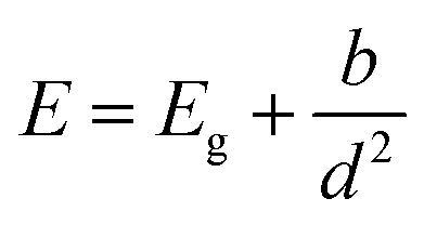
| Fig. 4 (a) Example of PL spectra prior to self-absorption correction for each sample, normalized to 1. (b) Peak PL energy with self-absorption correction (filled symbols) and without self-absorption correction (empty symbols) as a function of the relevant film height d, which is crystallite height for partially covered samples (diamonds) and optical thickness for fully covered samples (squares). The data are fitted with an equation for quantum confinement E = Eg + b/d2. The dashed line is the fit, and the shaded area is the 95% confidence limit. | ||
Even when self-absorption has been corrected for, the PL peak energy still shows considerable dependence on film thickness. Size dependence has previously been observed in perovskite nanocrystals due to the effect of quantum confinement which blue shifts the emission as the size of the nanocrystal is decreased.73–76 Wavelengths as low as 630 nm have been reported for colloidal nanocrystals of MAPbI3 with a diameter of 2.6 nm.75 Perovskite nanocrystals can also be made by templating in nanoporous silicon73,74 or alumina74 which show large shifts in PL wavelength with size, with similar values to our observations.73 The quantum confinement effect in MAPbI3 has already been shown to be strong in comparison to the equivalent Br and Cl perovskites due to its smaller effective exciton mass μ,74 and we believe this to be the most likely reason for the shifts we observe.
We fitted the dependence of the peak PL energy on film height with an equation for a quantum confined electronic system, shown in Fig. 4. We take the confinement to be in one dimension only, perpendicular to the film, which assumes that the diameter of the islands is greater than their height. The relevant dimension for confinement, d, is therefore the crystallite height for the films consisting of islands, and the optical thickness for the other films, which are distinguished by different markers in Fig. 4. It should be noted that the crystallite height and optical thickness are approximately equal in the second stage of growth. Where they differ for the two thickest films, the optical thickness is the most appropriate measure since we assume that the crystal boundaries, which represent a change in crystallographic orientation, do not electronically confine charges. The simplest equation for quantum confinement is the ‘particle in a box’ solution to the Schrodinger equation, which applies to free electrons and holes in a confined space. At room temperature, the exciton binding energy in bulk MAPbI3 is approximately 5 meV (ref. 77–79) (corresponding to a Bohr radius of ∼5 nm), meaning excitons spontaneously dissociate and we need only consider free electrons and holes. However for thinner material, the exciton binding energy will increase due to increased Coulomb interaction, both as a direct result of the proximity of electrons and holes, and also due to the change in effective dielectric constant which occurs when the film thickness is less than the Bohr radius, sometimes referred to as dielectric confinement80 or the image charge effect.81 Calculations have shown that this effect can be substantial in perovskite materials up to 30 Å thick,82 but should not be significant for our films which all have thickness greater than 7 nm. If the binding energy becomes large enough for there to be a significant presence of excitons at room temperature, then the equation must be modified to treat excitons rather than separate electrons and holes, known as the weak confinement regime.83 If the dimension of confinement is smaller than the exciton Bohr radius, the spatial correlation of the exciton is lost and the carriers can be treated as free electrons and holes, referred to as the strong confinement regime.83 A full analysis is beyond the scope of this study, but in all of these scenarios, the equation has the approximate form83
 64 and CsPbBr376 have yielded b = 12 eV nm2 and b = 2.6 eV nm2 respectively, though different metal halide perovskites are expected to have different values of b. These values are also calculated for nanocrystals, so charge carriers are confined in three dimensions. For the simple case of free carriers in an infinite spherical potential well, the lowest energy solution also gives b = ħ2π2/2μ when d is taken as the radius of the nanocrystal sphere. This may not be the case for more complex scenarios,83 but the comparison can at least confirm that our result falls close to the expected order of magnitude. There are two additional considerations which could affect the band gap energy – strain and chemical composition. DFT calculations have predicted a linear change in band gap with strain.85,86 A volume expansion corresponding to the change in lattice parameter between our least strained and most strained films is calculated to produce a band gap shift of 0.03 eV.85 This is much less than the change of over 0.1 eV that we observe, and we therefore consider strain effects to be negligible in comparison to the effect of quantum confinement. Photo-induced degradation can also cause a blue shift in PL wavelength, indicating a change in the lattice eventually leading to a conversion to PbI2.87 However, the XRD data show the films still had the perovskite structure at the time of measurement with no presence of PbI2.
Conclusions
In conclusion, we have monitored the incipient steps in the formation of MAPbI3 thin films fabricated by dual-source co-evaporation from an optical thickness of 2 nm to 320 nm. We found that the material initially forms crystallite islands of around 8 nm in height, which coalesce and build up strain. Once the substrate is completely covered, the crystallites grow in height uniformly and strain is released. We have demonstrated that photoluminescence from the thinnest MAPbI3 films fabricated by vapour deposition is dominated by quantum confinement, which therefore promises to be a useful fabrication method for nanoscale structures that can be implemented in efficient LEDs. With the growth procedure used in this work, light-emitting MAPbI3 films could be employed in an architecture incorporating 8 nm thick islands or a uniform layer of 10 nm or more. We note however that uniform growth of even thinner films should be easily within reach, e.g. through an optimization of perovskite-substrate interactions and growth conditions such as substrate temperature. Furthermore, an in-depth study using microscopy techniques such as electron microscopy and atomic force microscopy may allow for an investigation of the impact of the substrate on the film growth mechanism, provided these probes do not interfere with these relatively soft materials. Attempting epitaxial growth on a lattice matched substrate by vapour deposition would also provide a promising route towards ultra-thin layers suitable for multiple quantum wells or other heterostructures. Finally, we suggest that the Volmer–Weber type island growth mode observed in the early stages of the film growth may well be the cause of the small grain size that is typically encountered in co-evaporated perovskite films. We hence stipulate that the development of a method suitable for producing layer-by-layer growth may hold the key towards increasing crystallite grain size, and thus improving the efficiency and stability of solar cells fabricated though vapour deposition.Experimental details
Sample cleaning
Z-Cut quartz was washed with Hellmanex®, distilled water, acetone and isopropyl alcohol. Finally, the quartz was placed in an oxygen plasma asher for 10 minutes.Dual-source thermal evaporation
The films were fabricated using co-evaporation of PbI2 and CH3NH3I.27 500 mg each of CH3NH3I (synthesised as described in ref. 8) and PbI2 (ultra-dry 99.999% (metals basis), Alfa Aesar) were placed in separate crucibles, and the quartz discs were mounted on a rotating substrate holder to ensure that a uniform film was deposited. The temperature of the substrates was kept at 21 °C throughout the deposition. The chamber was allowed to reach a high vacuum (4 × 10⁻⁶ mbar), before the PbI2 and the CH3NH3I crucibles were heated to reach a steady rate, as monitored by the quartz crystal microbalance (QCM). Once the deposition rate had stabilized along with the pressure (4 × 10⁻⁶ mbar), the substrates were exposed to the vapour. The rates of both the CH3NH3I and PbI2 were calibrated, by analysis of the X-ray diffraction pattern of the thin film to ensure a 1:1 molar ratio was achieved in the final composition of the film. The deposition time was controlled by the programming of the substrate shutter to open and close after a specific time.
X-ray diffraction
The samples were mounted on a rotating sample holder in ambient conditions. 2θ measurements were performed using an X-ray diffractometer (Panalytical X'Pert Pro). The scan speed was 0.4° s−1 for 30 minutes (Cu-Kα radiation at λ = 1.54 Å) operating at 40 kV and 40 mA.Photoluminescence spectra
Samples were excited in ambient conditions with the aid of a tunable Ti:Sapphire pulsed (80 fs) laser, with its fundamental wavelength set to 1000 nm and an 80 MHz repetition rate (Mai Tai, Spectra-Physics). A BBO crystal was used to double the excitation frequency, giving an excitation wavelength of 500 nm. The 1000 nm fundamental wavelength was filtered out using a polarizer and a color filter. The excitation intensity was attenuated using an OD1 filter and a variable attenuator consisting of a waveplate and a vertical polariser to achieve 0.5 mW over a beam size of 0.09 mm2. A horizontal polariser and a 590 nm long-pass color filter were placed after the sample to remove any laser scatter from the spectrum. Photoluminescence from the sample was collected by a pair of off-axis parabolic mirrors and focused onto the entry slit of a grating monochromator (Triax, Horiba). The spectrally resolved PL was detected by a nitrogen-cooled Si-CCD detector (Symphony, Horiba) and the spectral response of all components was corrected for using a tungsten filament lamp with known spectrum.Optical absorption
Visible to near infrared (NIR) transmission and reflection measurements were performed using a Fourier transform infrared spectrometer (Vertex 80v, Bruker). A tungsten halogen lamp was used as a light source, and the light passing through the sample (T) and reflected from the sample (R) was detected by a silicon diode detector. The empty holder, and a silver mirror were used as references for 100% transmission and reflection respectively. A blank quartz substrate was also measured to correct for its own absorption.Conflicts of interest
There are no conflicts to declare.Acknowledgements
The authors acknowledge the Engineering and Physical Sciences Research Council (EPSRC) for financial support. L. M. H. thanks the Alexander von Humboldt Foundation for support through a Friedrich Wilhelm Bessel Research Award. E. S. P. thanks the EPSRC Centre for Doctoral Training in New and Sustainable Photovoltaics (CDT-PV) for support through a doctoral studentship.Notes and references
- S. Razza, S. Castro-Hermosa, A. Di Carlo and T. M. Brown, APL Mater., 2016, 4, 091508 CrossRef.
- G. E. Eperon, S. D. Stranks, C. Menelaou, M. B. Johnston, L. M. Herz and H. J. Snaith, Energy Environ. Sci., 2014, 7, 982–988 RSC.
- D. Ju, Y. Dang, Z. Zhu, H. Liu, C. Chueh, X. Li, L. Wang, X. Hu, A. K.-Y. Jen and X. Tao, Chem. Mater., 2018, 30, 1556–1565 CrossRef CAS.
- R. J. Sutton, G. E. Eperon, L. Miranda, E. S. Parrott, B. A. Kamino, J. B. Patel, M. T. Hörantner, M. B. Johnston, A. A. Haghighirad, D. T. Moore and H. J. Snaith, Adv. Energy Mater., 2016, 6, 1502458 CrossRef.
- F. Hao, C. C. Stoumpos, R. P. H. Chang and M. G. Kanatzidis, J. Am. Chem. Soc., 2014, 136, 8094–8099 CrossRef CAS.
- I. L. Braly, D. W. Dequilettes, L. M. Pazos-Outón, S. Burke, M. E. Ziffer, D. S. Ginger and H. W. Hillhouse, Nat. Photonics, 2018, 12, 355–361 CrossRef CAS.
- L. M. Herz, ACS Energy Lett., 2017, 2, 1539–1548 CrossRef CAS.
- M. Liu, M. B. Johnston and H. J. Snaith, Nature, 2013, 501, 395–398 CrossRef CAS PubMed.
- H. J. Snaith, J. Phys. Chem. Lett., 2013, 4, 3623–3630 CrossRef CAS.
- W. S. Yang, B.-W. Park, E. H. Jung, N. J. Jeon, Y. C. Kim, D. U. Lee, S. S. Shin, J. Seo, E. K. Kim, J. H. Noh and S. Il Seok, Science, 2017, 356, 1376–1379 CrossRef CAS PubMed.
- W. Tress, Adv. Energy Mater., 2017, 7, 1602358 CrossRef.
- S. D. Stranks and H. J. Snaith, Nat. Nanotechnol., 2015, 10, 391–402 CrossRef CAS.
- Z. Xiao, R. A. Kerner, L. Zhao, N. L. Tran, K. M. Lee, T. W. Koh, G. D. Scholes and B. P. Rand, Nat. Photonics, 2017, 11, 108–115 CrossRef CAS.
- N. Wang, L. Cheng, R. Ge, S. Zhang, Y. Miao, W. Zou, C. Yi, Y. Sun, Y. Cao, R. Yang, Y. Wei, Q. Guo, Y. Ke, M. Yu, Y. Jin, Y. Liu, Q. Ding, D. Di, L. Yang, G. Xing, H. Tian, C. Jin, F. Gao, R. H. Friend, J. Wang and W. Huang, Nat. Photonics, 2016, 10, 699–704 CrossRef CAS.
- Q. Zhang, S. T. Ha, X. Liu, T. C. Sum and Q. Xiong, Nano Lett., 2014, 14, 5995–6001 CrossRef CAS PubMed.
- L. Zhang, F. Yuan, H. Dong, B. Jiao, W. Zhang, X. Hou, S. Wang, Q. Gong and Z. Wu, ACS Appl. Mater. Interfaces, 2018, 10, 40661–40671 CrossRef CAS PubMed.
- J. Borchert, R. L. Milot, J. B. Patel, C. L. Davies, A. D. Wright, L. Martínez Maestro, H. J. Snaith, L. M. Herz and M. B. Johnston, ACS Energy Lett., 2017, 2, 2799–2804 CrossRef CAS.
- T. W. Crothers, R. L. Milot, J. B. Patel, E. S. Parrott, J. Schlipf, P. Müller-Buschbaum, M. B. Johnston and L. M. Herz, Nano Lett., 2017, 17, 5782–5789 CrossRef CAS.
- J. B. Patel, Q. Lin, O. Zadvorna, C. L. Davies, L. M. Herz and M. B. Johnston, J. Phys. Chem. Lett., 2018, 9, 263–268 CrossRef CAS PubMed.
- C. Roldán-Carmona, O. Malinkiewicz, R. Betancur, G. Longo, C. Momblona, F. Jaramillo, L. Camacho and H. J. Bolink, Energy Environ. Sci., 2014, 7, 2968–2973 RSC.
- C. Roldán-Carmona, O. Malinkiewicz, A. Soriano, G. Mínguez Espallargas, A. Garcia, P. Reinecke, T. Kroyer, M. I. Dar, M. K. Nazeeruddin and H. J. Bolink, Energy Environ. Sci., 2014, 7, 994–997 RSC.
- F. Sahli, J. Werner, B. A. Kamino, M. Bräuninger, R. Monnard, B. Paviet-Salomon, L. Barraud, L. Ding, J. J. D. Leon, D. Sacchetto, G. Cattaneo, M. Boccard, M. Despeisse, S. Nicolay, Q. Jeangros, B. Niesen and C. Ballif, Nat. Mater., 2018, 17, 820–826 CrossRef CAS PubMed.
- J. B. Patel, R. L. Milot, A. D. Wright, L. M. Herz and M. B. Johnston, J. Phys. Chem. Lett., 2016, 7, 96–102 CrossRef CAS PubMed.
- D. Yang, Z. Yang, W. Qin, Y. Zhang, S. Liu and C. Li, J. Mater. Chem. A, 2015, 3, 9401–9405 RSC.
- K. A. Bush, N. Rolston, A. Gold-Parker, S. Manzoor, J. Hausele, Z. Yu, J. A. Raiford, R. Cheacharoen, Z. C. Holman, M. F. Toney, R. H. Dauskardt and M. D. McGehee, ACS Energy Lett., 2018, 3, 1225–1232 CrossRef CAS.
- J. Zhao, Y. Deng, H. Wei, X. Zheng, Z. Yu, Y. Shao, J. E. Shield and J. Huang, Sci. Adv., 2017, 3, eaao5616 CrossRef.
- J. B. Patel, J. Wong-Leung, S. Van Reenen, N. Sakai, J. T. W. Wang, E. S. Parrott, M. Liu, H. J. Snaith, L. M. Herz and M. B. Johnston, Adv. Electron. Mater., 2017, 3, 1600470 CrossRef.
- C. Momblona, L. Gil-Escrig, E. Bandiello, E. M. Hutter, M. Sessolo, K. Lederer, J. Blochwitz-Nimoth and H. J. Bolink, Energy Environ. Sci., 2016, 9, 3456–3463 RSC.
- J. H. Heo, D. H. Song and S. H. Im, Adv. Mater., 2014, 26, 8179–8183 CrossRef CAS.
- Q. Jiang, Z. Chu, P. Wang, X. Yang, H. Liu, Y. Wang, Z. Yin, J. Wu, X. Zhang and J. You, Adv. Mater., 2017, 29, 1703852 CrossRef.
- C. Bi, Q. Wang, Y. Shao, Y. Yuan, Z. Xiao and J. Huang, Nat. Commun., 2015, 6, 7747 CrossRef CAS.
- M. U. Rothmann, W. Li, J. Etheridge and Y. B. Cheng, Adv. Energy Mater., 2017, 7, 1700912 CrossRef.
- C. H. Chiang and C. G. Wu, ChemSusChem, 2016, 9, 2666–2672 CrossRef CAS.
- Z. Chu, M. Yang, P. Schulz, D. Wu, X. Ma, E. Seifert, L. Sun, X. Li, K. Zhu and K. Lai, Nat. Commun., 2017, 8, 2230 CrossRef PubMed.
- A. Ioakeimidis, C. Christodoulou, M. Lux-Steiner and K. Fostiropoulos, J. Solid State Chem., 2016, 244, 20–24 CrossRef CAS.
- J. Ávila, C. Momblona, P. P. Boix, M. Sessolo and H. J. Bolink, Joule, 2017, 1, 431–442 CrossRef.
- H. Wang, Z. Bao, H. Tsai, A. Tang and R. Liu, Small, 2017, 14, 1702433 CrossRef.
- K. Lin, J. Xing, L. N. Quan, F. P. G. de Arquer, X. Gong, J. Lu, L. Xie, W. Zhao, D. Zhang, C. Yan, W. Li, X. Liu, Y. Lu, J. Kirman, E. H. Sargent, Q. Xiong and Z. Wei, Nature, 2018, 562, 245–248 CrossRef CAS.
- M. Ban, Y. Zou, J. P. H. Rivett, Y. Yang, T. H. Thomas, Y. Tan, T. Song, X. Gao, D. Credington, F. Deschler, H. Sirringhaus and B. Sun, Nat. Commun., 2018, 9, 3892 CrossRef.
- X. Zhang, M. Lu, Y. Zhang, H. Wu, X. Shen, W. Zhang, W. Zheng, V. L. Colvin and W. W. Yu, ACS Cent. Sci., 2018, 4, 1352–1159 CrossRef CAS PubMed.
- R. Quintero-Bermudez, A. Gold-Parker, A. H. Proppe, R. Munir, Z. Yang, S. O. Kelley, A. Amassian, M. F. Toney and E. H. Sargent, Nat. Mater., 2018, 17, 900–907 CrossRef CAS.
- L. Polavarapu, B. Nickel, J. Feldmann and A. S. Urban, Adv. Energy Mater., 2017, 7, 1700267 CrossRef.
- Y. Narukawa, M. Ichikawa, D. Sanga, M. Sano and T. Mukai, J. Phys. D: Appl. Phys., 2010, 43, 354002 CrossRef.
- L. Zhao, K. M. Lee, K. Roh, S. U. Z. Khan and B. P. Rand, Adv. Mater., 2018, 1805836 Search PubMed.
- Z.-K. Tan, R. S. Moghaddam, M. L. Lai, P. Docampo, R. Higler, F. Deschler, M. Price, A. Sadhanala, L. M. Pazos, D. Credgington, F. Hanusch, T. Bein, H. J. Snaith and R. H. Friend, Nat. Nanotechnol., 2014, 9, 1–6 CrossRef.
- L. Gil-Escrig, A. Miquel-Sempere, M. Sessolo and H. J. Bolink, J. Phys. Chem. Lett., 2015, 6, 3743–3748 CrossRef CAS.
- A. Genco, F. Mariano, S. Carallo, V. L. P. Guerra, S. Gambino, D. Simeone, A. Listorti, S. Colella, G. Gigli and M. Mazzeo, Adv. Electron. Mater., 2016, 2, 1500325 CrossRef.
- B. Yang, O. Dyck, W. Ming, M.-H. Du, S. Das, C. M. Rouleau, G. Duscher, D. B. Geohegan and K. Xiao, ACS Appl. Mater. Interfaces, 2016, 8, 32333–32340 CrossRef CAS.
- P. Pistor, J. Borchert, W. Fra, R. Csuk and R. Scheer, J. Phys. Chem. Lett., 2014, 5, 3308–3312 CrossRef CAS.
- P. Pistor, T. Burwig, C. Brzuska, B. Weber and W. Fränzel, J. Mater. Chem. A, 2018, 6, 11496–11506 RSC.
- H. Xu, Y. Wu, J. Cui, C. Ni, F. Xu, J. Cai, F. Hong, Z. Fang, W. Wang, J. Zhu, L. Wang, R. Xu and F. Xu, Phys. Chem. Chem. Phys., 2016, 18, 18607–18613 RSC.
- S. Olthof and K. Meerholz, Sci. Rep., 2017, 7, 40267 CrossRef CAS.
- X. Zhou, X. Li, Y. Liu, F. Huang and D. Zhong, Appl. Phys. Lett., 2016, 108, 121601 CrossRef.
- J. Feng, APL Mater., 2014, 2, 081801 CrossRef.
- T. Baikie, Y. Fang, J. M. Kadro, M. Schreyer, F. Wei, S. G. Mhaisalkar, M. Graetzel and T. J. White, J. Mater. Chem. A, 2013, 1, 5628 RSC.
- Y. Liu, Z. Yang, D. Cui, X. Ren, J. Sun, X. Liu, J. Zhang, Q. Wei, H. Fan, F. Yu, X. Zhang, C. Zhao and S. F. Liu, Adv. Mater., 2015, 27, 5176–5183 CrossRef CAS.
- Y. Dang, Y. Liu, Y. Sun, D. Yuan, X. Liu, W. Lu, G. Liu, H. Xia and X. Tao, CrystEngComm, 2015, 17, 665–670 RSC.
- R. C. Cammarata, T. M. Trimble and D. J. Srolovitz, J. Mater. Res., 2000, 15, 2468–2474 CrossRef CAS.
- J. A. Thornton, Thin Solid Films, 1989, 171, 5–31 CrossRef.
- R. C. Cammarata, Prog. Surf. Sci., 1994, 46, 1–38 CrossRef CAS.
- E. Chason and P. R. Guduru, J. Appl. Phys., 2016, 119, 191101 CrossRef.
- L. Niu, Q. Zeng, J. Shi, C. Cong, C. Wu, F. Liu, J. Zhou, W. Fu, Q. Fu, C. Jin, T. Yu, X. Liu and Z. Liu, Adv. Funct. Mater., 2016, 26, 5263–5270 CrossRef CAS.
- P. Scherrer, Nachr. Ges. Wiss. Goettingen, Math.-Phys. Kl., 1918, 2, 98–100 Search PubMed.
- D. Di, K. P. Musselman, G. Li, A. Sadhanala, Y. Ievskaya, Q. Song, Z.-K. Tan, M. L. Lai, J. L. MacManus-Driscoll, N. C. Greenham and R. H. Friend, J. Phys. Chem. Lett., 2015, 6, 446–450 CrossRef CAS.
- W. H. Hall, Proc. Phys. Soc., London, Sect. A, 1949, 62, 741–743 CrossRef.
- J. T. W. Wang, Z. Wang, S. Pathak, W. Zhang, D. W. Dequilettes, F. Wisnivesky-Rocca-Rivarola, J. Huang, P. K. Nayak, J. B. Patel, H. A. Mohd Yusof, Y. Vaynzof, R. Zhu, I. Ramirez, J. Zhang, C. Ducati, C. Grovenor, M. B. Johnston, D. S. Ginger, R. J. Nicholas and H. J. Snaith, Energy Environ. Sci., 2016, 9, 2892–2901 RSC.
- D. P. McMeekin, Z. Wang, W. Rehman, F. Pulvirenti, J. B. Patel, N. K. Noel, M. B. Johnston, S. R. Marder, L. M. Herz and H. J. Snaith, Adv. Mater., 2017, 29, 1607039 CrossRef.
- N. Rolston, B. L. Watson and R. H. Dauskardt, Extreme Mech. Lett., 2016, 9, 353–358 CrossRef.
- I. N. Stranski and L. Krastanow, Abh. Math. Kl. IIb, 1938, 146, 797–810 CAS.
- K. Reichelt and X. Jiang, Thin Solid Films, 1990, 191, 91–126 CrossRef.
- Y. Wang, X. Sun, Z. Chen, Y. Sun, S. Zhang, T. Lu, E. Wertz and J. Shi, Adv. Mater., 2017, 29, 1702643 CrossRef.
- Y. Wang, L. Gao, Y. Yang, Y. Xiang, Z. Chen, Y. Dong, H. Zhou, Z. Cai, G. Wang and J. Shi, Phys. Rev. Mater., 2018, 2, 076002 CrossRef CAS.
- V. Malgras, J. Henzie, T. Takei and Y. Yamauchi, Chem. Commun., 2017, 53, 2359–2362 RSC.
- S. Demchyshyn, J. M. Roemer, H. Groiß, H. Heilbrunner, C. Ulbricht, D. Apaydin, A. Böhm, U. Rütt, F. Bertram, G. Hesser, M. C. Scharber, N. S. Sariciftci, B. Nickel, S. Bauer, E. D. Głowacki and M. Kaltenbrunner, Sci. Adv., 2017, 3, e1700738 CrossRef.
- L. Wang, N. E. Williams, E. W. Malachosky, J. P. Otto, D. Hayes, R. E. Wood, P. Guyot-Sionnest and G. S. Engel, ACS Nano, 2017, 11, 2689–2696 CrossRef CAS.
- L. Protesescu, S. Yakunin, M. I. Bodnarchuk, F. Krieg, R. Caputo, C. H. Hendon, R. X. Yang, A. Walsh and M. V. Kovalenko, Nano Lett., 2015, 15, 3692–3696 CrossRef CAS.
- A. Miyata, A. Mitioglu, P. Plochocka, O. Portugall, J. T.-W. Wang, S. D. Stranks, H. J. Snaith and R. J. Nicholas, Nat. Phys., 2015, 11, 582–587 Search PubMed.
- C. L. Davies, M. R. Filip, J. B. Patel, T. W. Crothers, C. Verdi, A. D. Wright, R. L. Milot, F. Giustino, M. B. Johnston and L. M. Herz, Nat. Commun., 2018, 9, 293 Search PubMed.
- J. Even, L. Pedesseau and C. Katan, J. Phys. Chem. C, 2014, 118, 11566–11572 CrossRef CAS.
- L. V. Keldysh, Sov. J. Exp. Theor. Phys. Lett., 1979, 29, 658 Search PubMed.
- K. Tanaka, T. Takahashi, T. Kondo, T. Umebayashi, K. Asai and K. Ema, Phys. Rev. B: Condens. Matter Mater. Phys., 2005, 71, 045312 CrossRef.
- D. Sapori, M. Kepenekian, L. Pedesseau, C. Katan and J. Even, Nanoscale, 2016, 8, 6369–6378 RSC.
- Y. Kayanuma, Phys. Rev. B: Condens. Matter Mater. Phys., 1988, 38, 9797–9805 CrossRef.
- A. Buin, R. Comin, A. H. Ip and E. H. Sargent, J. Phys. Chem. C, 2015, 119, 13965–13971 CrossRef CAS.
- M. I. Dar, G. Jacopin, S. Meloni, A. Mattoni, N. Arora, A. Boziki, S. M. Zakeeruddin, U. Rothlisberger and M. Gratzel, Sci. Adv., 2016, 2, e1601156 CrossRef.
- C. Grote, R. F. Berger, D. W. DeQuilettes, S. Koch, S. Burke, R. Paranji, A. J. Shropshire, M. E. Ziffer and D. S. Ginger, J. Phys. Chem. C, 2015, 119, 22832–22837 CrossRef CAS.
- A. Merdasa, M. Bag, Y. Tian, E. Källman, A. Dobrovolsky and I. G. Scheblykin, J. Phys. Chem. C, 2016, 120, 10711–10719 CrossRef CAS.
Footnote |
| † Electronic supplementary information (ESI) available: Optical thickness determination; XRD analysis; correction of PL for self-absorption. See DOI: 10.1039/c9nr04104d |
| This journal is © The Royal Society of Chemistry 2019 |