
 Open Access Article
 This Open Access Article is licensed under a
 Creative Commons Attribution 3.0 Unported Licence
Efficient light harvesting in hybrid quantum dot–interdigitated back contact solar cells via resonant energy transfer and luminescent downshifting†
Chirenjeevi
Krishnan
 *a,
Thomas
Mercier
a,
Tasmiat
Rahman
a,
Giacomo
Piana
b,
Mael
Brossard
c,
Timur
Yagafarov
c,
Alexander
To
d,
Michael E.
Pollard
d,
Peter
Shaw
a,
Darren M.
Bagnall
e,
Bram
Hoex
d,
Stuart A.
Boden
a,
Pavlos G.
Lagoudakis
bc and
Martin D. B.
Charlton
a
*a,
Thomas
Mercier
a,
Tasmiat
Rahman
a,
Giacomo
Piana
b,
Mael
Brossard
c,
Timur
Yagafarov
c,
Alexander
To
d,
Michael E.
Pollard
d,
Peter
Shaw
a,
Darren M.
Bagnall
e,
Bram
Hoex
d,
Stuart A.
Boden
a,
Pavlos G.
Lagoudakis
bc and
Martin D. B.
Charlton
a
aSchool of Electronics and Computer Science, University of Southampton, SO17 1BJ Southampton, UK. E-mail: c.krishnan@soton.ac.uk
bSchool of Physics and Astronomy, University of Southampton, SO17 1BJ Southampton, UK
cCentre for Photonics and Quantum Materials, Skolkovo Institute of Science and Technology, Moscow 143026, Russia
dSchool of Photovoltaic and Renewable Energy Engineering, University of New South Wales, Kensington, NSW2052, Australia
eSchool of Engineering, Macquarie University, Sydney, NSW2109, Australia
First published on 9th October 2019
Abstract
In this paper, we propose a hybrid quantum dot (QD)/solar cell configuration to improve performance of interdigitated back contact (IBC) silicon solar cells, resulting in 39.5% relative boost in the short-circuit current (JSC) through efficient utilisation of resonant energy transfer (RET) and luminescent downshifting (LDS). A uniform layer of CdSe1−xSx/ZnS quantum dots is deposited onto the AlOx surface passivation layer of the IBC solar cell. QD hybridization is found to cause a broadband improvement in the solar cell external quantum efficiency. Enhancement over the QD absorption wavelength range is shown to result from LDS. This is confirmed by significant boosts in the solar cell internal quantum efficiency (IQE) due to the presence of QDs. Enhancement over the red and near-infrared spectral range is shown to result from the anti-reflection properties of the QD layer coating. A study on the effect of QD layer thickness on solar cell performance was performed and an optimised QD layer thickness was determined. Time-resolved photoluminescence (TRPL) spectroscopy was used to investigate the photoluminescence dynamics of the QD layer as a function of AlOx spacer layer thickness. RET can be evoked between the QD and Si layers for very thin AlOx spacer layers, with RET efficiencies of up to 15%. In the conventional LDS architecture, down-converters are deposited on the surface of an optimised anti-reflection layer, providing relatively narrowband enhancement, whereas the QDs in our hybrid architecture provide optical enhancement over the broadband wavelength range, by simultaneously utilising LDS, RET-mediated carrier injection, and antireflection effects, resulting in up to 40% improvement in the power conversion efficiency (PCE). Low-cost synthesis of QDs and simple device integration provide a cost-effective solution for boosting solar cell performance.
1. Introduction
Ever-increasing global energy demands have put tremendous pressure on current natural resources, creating a growing need for cheap and efficient renewable energy. Photovoltaic technologies have shown great promise to tackle these challenges with global energy production capacity exceeding 500 GW in 20181 and rapidly growing. With a market share of over 90% and lab power conversion efficiency (PCE) exceeding 26%,2 silicon (Si) solar cells currently dominate the industry. As the extraction efficiency for photo-generated carriers is near the theoretical limit for such devices, new light management approaches are required to bring cell efficiencies closer to their 29% Shockley–Queisser limit.3In recent years, colloidal quantum dot (QD)-based solar cells have seen a rapid increase in performance, with PCE now reaching up to 13.4%.4 It has also been predicted that perfectly stacked QD layers with different band gaps can reach a maximum cell efficiency of 66%.5 QD-based solar cells could also benefit from multiple exciton generation (MEG),6 where two or more electron hole pairs are generated upon absorption of a photon with energy greater than the bandgap. MEG has also been demonstrated in a nano-rod solar cell,7 showing external quantum efficiency (EQE) exceeding 120%. QDs possess unique properties of bandgap tunability and high absorption cross section compared to bulk semiconductor materials. The transport and extraction of carriers through the QD layer has been the hindrance in utilizing the full potential of QDs. While recent advances have partly mitigated such transport issues leading to a steady increase of the PCE of QD solar cells since 2010,8 pure QD solar cells are unlikely to be able to directly compete with Si technology in the near future. An alternative architecture uses QD absorbers in proximity to conventional solar cells. Photons absorbed in the QDs can then be efficiently transferred to the high-mobility semiconductor of a solar cell through resonant energy transfer (RET) or radiative transfer. In the RET process, the electron–hole pairs are generated in the QDs and are transferred to the underlying semiconductor via dipole–dipole coupling. No photons are involved in the energy transfer process. Such an architecture has been shown to improve the performance of InGaP solar cells9 and, in the reverse configuration, of GaN LEDs.10 Radiative combination is in contrast the basis for luminescent downshifting (LDS). In this case, high-energy photons are absorbed by a luminescent material (such as QDs) which re-emits at a lower energy more efficiently utilized by the solar cell. Commercial adoption of LDS technology has been so far limited by the relatively low photoluminescence quantum yield (PLQY) and the need of cell architectures9,11 to carefully consider all light management aspects. Recent advancements in QD technology leveraging such effects as quantum cutting have made possible PLQYs greater than 140%,12,13 thus unlocking the tantalizing prospect of multi-photon LDS. Such an architecture could prove extremely efficient with theoretical solar conversion efficiencies reaching up to 39.63% for single junction cells.12
In conventional LDS approaches, downshifting particles are embedded into an SiO2 matrix or deposited directly onto the surface of the anti-reflection (AR) layer. Such configurations have resulted in low PCE enhancements,13,14 as depositing a significant amount of LDS material damages the AR properties of the cell. Record silicon solar cell efficiencies have been reported for interdigitated back contact (IBC) architecture.2,15 In IBC solar cells, charge carrier separation and collection happen at the rear of the solar cell.
While highly efficient for green to red photons (absorbed in the bulk of the cell), IBC solar cells suffer from relatively poor extraction efficiencies for high-energy blue photons (absorbed near the surface of the cell, far away from the junction region). This results in a sharp drop of the External Quantum Efficiency (EQE) below 550 nm,16 making it a perfect platform for LDS enhancement. By having a top surface free of any contacts or doped regions, IBC solar cells are also ideal for investigating photon management structures. Photon management strategies based on nanostructures such as nanowire arrays,17–19 nanoholes,20 and pyramid arrays have previously been proposed. Using QDs on their own or combining them with photon management structures and textured surfaces could pave the way for new efficient hybrid photovoltaic technologies. In this paper, we demonstrate efficient hybrid QD–IBC architectures to improve the performance of silicon solar cells. The CdSe1−xSx/ZnS QDs with a peak emission of 533 ± 15 nm are deposited onto the top passivation layer (AlOx) of planar IBC solar cells. QDs act as a strong absorber for near-UV and visible photons below 500 nm, generating electron–hole pairs. On annihilation, photons are emitted which are then efficiently absorbed in the IBC solar cell. The QD layers act as a single anti-reflection coating, reducing the reflection and increasing the absorption of the solar cell. We achieve a 40% relative boost in PCE due to enhanced photocurrent.
2. Results and discussion
A schematic of the hybrid photovoltaic (PV) device studied in this work is shown in Fig. 1(a). It is a planar (non-textured) interdigitated back contact (IBC) silicon solar cell with an 18 nm thick AlOx front surface passivation layer. CdSe1−xSx/ZnS (core/shell) QDs are deposited onto the AlOx layer, as shown in the cross-sectional SEM image in Fig. 1(b). The inset shows the front and rear photographs of an IBC solar cell, illustrating the interdigitated contact fingers. The fabrication of the hybrid planar IBC solar cell is described in detail in the Experimental section. QDs of the structure CdSe1−xSx/ZnS were selected over other candidates to be used as the QD component in this device due to their exceptional photochemical stabilities,21 high photoluminescence quantum yields, and emission close to the short fall in the EQE of the IBC solar cell.16 We have also shown in prior work10 that CdSe1−xSx/ZnS QDs are compatible with RET activity, rendering them an ideal component worthy of device integration and further study. Fig. 2(a) shows the absorption and photoluminescence (PL) spectra of the CdSe1−xSx/ZnS QDs deposited onto a glass slide. The QDs have a 1s absorption peak at 502 nm, increasing exponentially towards the ultraviolet (UV) part of the spectrum. On excitation with a 400 nm laser source, the QDs have PL emission at 533 nm, with a full width at half maximum (FWHM) of 30 nm. These QDs were selected for their high PLQY throughout the absorption spectral bandwidth. Fig. 2(b) shows the PLQY of CdSe1−xSx/ZnS QDs dissolved in toluene for a concentration of 0.16 mg ml−1. The QDs have a PLQY of 86% at 370 nm that linearly drops and plateaus at 79 ± 1% between 420 nm and 490 nm. The optical constants of the CdSe1−xSx/ZnS QDs (Fig. 2(c)) were measured and modelled on a Si substrate using a J. A. Woollam M-2000 ellipsometer. These data were subsequently used in OPAL222 to model the absorption for different QD layer thicknesses (Fig. 2(d)) on Si. As the thickness increases from 6 nm to 36 nm, the absorption increases. Increasing the QD layer thickness further results in reflection at the QD–Si interface, influencing the absorption.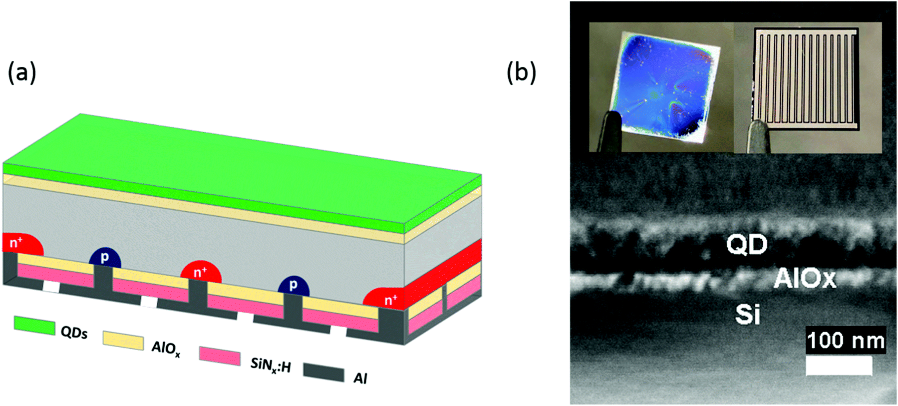 | ||
| Fig. 1 (a) Schematic representation of the hybrid planar IBC solar cell and (b) the cross-sectional SEM image of QDs and AlOx on the IBC solar cell, where the inset photo shows the front and rear of the cell. | ||
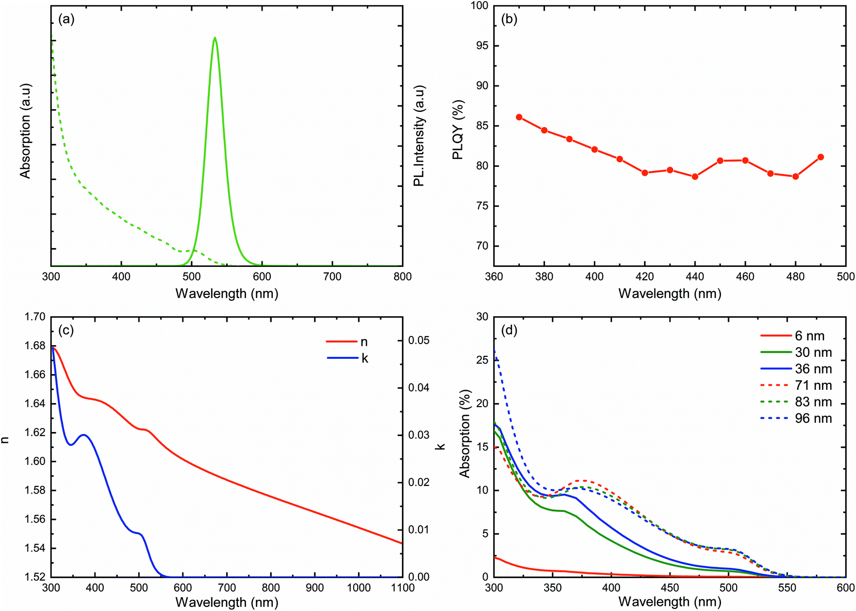 | ||
| Fig. 2 (a) Absorption (dashed line) and photoluminescence (solid line) of CdSe1−xSx/ZnS QDs deposited on a glass slide, (b) measured PLQY of CdSe1−xSx/ZnS QDs in solution for a concentration of 0.16 mg ml−1, (c) optical constants of CdSe1−xSx/ZnS QDs, and (d) modelled absorption for different thicknesses of the QD layer on Si. | ||
The current–voltage (I–V) characteristics of a solar cell before and after hybridisation with a 32 ± 2 nm and a 70 ± 3 nm thick QD layer under 1 sun illumination are presented in Fig. 3(a). Hybridisation is found to increase the short-circuit current (Jsc) by 17%, from 23.28 mA cm−2 to 27.29 mA cm−2, driving a sharp increase of the PCE from 11.1% to 13.0% and a relative enhancement of 12%. Increasing the QD layer thickness to 70 ± 3 nm is shown to further increase the performance of the hybrid device, boosting the JSC by 30% to 30.25 mA cm−2 and the PCE by 32% to 14.7%. A QD layer thickness dependence study was performed on a different device and the relative enhancements in the JSC and PCE are presented in Fig. 3(b). The absolute JSC and PCE for this device is shown in the ESI.† Both PCE and JSC are shown to linearly increase with the QD layer thickness, reaching a clear optimum at 83 ± 3 nm. This optimum device shows a dramatic hybridization enhancement of the PCE, increasing by 40% compared to the bare device, and of the Jsc, increasing by 39.5% compared to the bare device. PCE and Jsc start to drop for thicker QD films above this optimum point, a sign that parasitic absorption in the thick QD layer starts becoming detrimental to the overall performance of the cell. The parasitic absorption denotes here re-absorption in the subsequent layer of QDs, which is significant in thicker layers. First, due to the strong dependence of RET on distance, a thicker layer would diminish the efficiency of transfer from the QDs on the surface. This then increases dependence on the radiative transfer of energy, thus, as a result, there is further loss due to absorption–reabsorption interactions as down-shifted light is forced through multiple interactions in the thicker film. This, coupled with the moving away from the optimum AR film thickness, leads to a drop in JSC for the thickest QD layer (Fig. 3(b)). Voc and fill factor (FF) were found to be independent of the QD layer thickness, with average values of 0.616 ± 0.006 V and 78.57%, respectively. The corresponding parameters are available in the ESI.† Having a PCE enhancement fully driven by a JSC increase is a clear indicator that the QDs only affect the optical properties of the cell, without modifying its electrical properties.
 | ||
| Fig. 3 (a) J–V curves of the IBC solar cell before and after hybridization of our best device. (b) Relative variations of short-circuit current (Jsc) and power conversion efficiency (PCE) of the solar cell for different QD layer thicknesses. (c) EQE of hybrid IBC solar cells for different QD layer thicknesses. (d) Reflectance of the hybrid IBC solar cell for different thicknesses of QDs. The EQE shown here was measured under 1 sun light bias. | ||
The spectral response of the solar cell before and after QDs gives insight into the boosting mechanism in our hybrid PV device. Under 1 sun bias, the EQE of the IBC (Fig. 3(c)) solar cell was investigated for different QD layer thicknesses. The boost in the EQE of the hybrid PV devices can be categorized into two spectral bandwidth ranges: (1) where QDs absorb the incoming photons (300 nm–550 nm) and (2) in the wavelength region where the QDs are transparent (550 nm–1100 nm). To avoid any disparity in the results, the same IBC solar cell was used for measuring the EQE for different QD layer thicknesses. After hybridization of the IBC solar cell with a 6 nm thick QD layer, we observe an EQE improvement over a broad wavelength range of 300 nm to 925 nm; see Fig. 3(c). By increasing the QD layer thickness to 30 nm, the enhancement in EQE is observed over the entire measured spectrum of 300 nm to 1100 nm. In the wavelength range where QDs absorb efficiently, see Fig. 2(a) and (c), enhancement is due to an LDS mechanism. Above 550 nm where QDs do not absorb well, the enhancement can be attributed to increased optical coupling of light into the solar cell as a result of an antireflection (AR) effect. As the QD film thickness increases from 64 nm to 83 nm, the maximum enhancement in EQE shifts to longer wavelengths. The red shift in EQE enhancement with the QD layer thickness is similar to the behavior of an antireflective coating on a solar cell. The reflectance spectra of the IBC solar cell before and after hybridization with different QD thicknesses, see Fig. 3(d), were recorded to understand the influence of the anti-reflection coatings. The overall reflectance of the IBC cell decreases with increasing QD layer thickness from 6 nm to 30 nm. When the thickness is increased from 64 nm to 83 nm, the drop in reflectance with QD film thickness is consistent with the boost in EQE. For better understanding, the reflectance of QDs on Si was modelled using OPAL222 which resulted in an 82 nm thick QD layer being the optimum thickness for anti-reflection. This QD layer thickness is the same as our best hybrid IBC cell with a QD film thickness of 83 nm, see Fig. 3(b). The EQE of our hybrid PV is strongly influenced by the AR effect of the QD layer on Si.
The QD layer also absorbs photons and transfer them to underlying silicon, which influences the performance of our hybrid IBC solar cell. The existence of LDS in the hybrid IBC solar can be determined from the influence of QDs on the internal quantum efficiency (IQE)9 of the IBC solar cell, which is determined from the ratio of unbiased EQE measurement and reflectance of the solar cell. Fig. 4 shows the relative change in the IQE of the IBC solar cell after deposition of a 32 ± 2 nm thick QD layer. Hybridization significantly boosts the IQE of the IBC solar cell with maximum relative enhancement above 100% at 415 nm. The enhancement in IQE follows the absorption spectra of CdSe1−xSx/ZnS QDs and drops to near zero above the absorption spectral range (Fig. 2(a) and (c)). The EQE enhancement due to different mechanisms can be quantified by modelling the EQE enhancement due to anti-reflection. Using the IQE of the planar IBC solar cell and modelled reflectance of QDs/AlOx/Si, the relative EQE enhancement from a 32 nm thick QD layer was determined (Fig. 4). On comparing the relative change in the EQE of modelled data with the measured one, there is an additional 125% boost in EQE greater than that provided by the AR effect at 400 nm. The EQE enhancement due to LDS and RET is observed over the spectral range in which the QDs absorb. On weighting the unbiased EQE of modelled and measured spectra with AM1.5G in the absorption region of the QDs, there is a 40% boost in JSC due to combined AR, LDS, and RET mechanisms, of which 17% enhancement is due to LDS and RET and 23% enhancement is due to the AR effect.
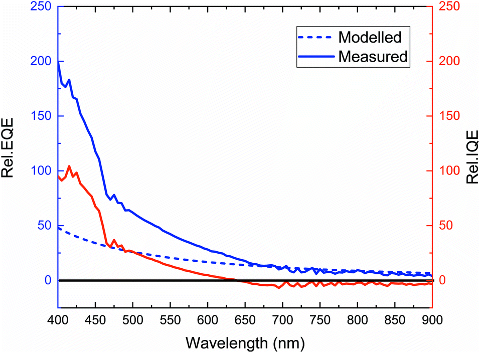 | ||
| Fig. 4 Relative enhancement in IQE (red solid line) and EQE (blue solid line) after deposition of a 32 nm thick QD layer. The blue dashed line is the modelled EQE enhancement due to antireflection. The EQE and IQE spectral responses shown were measured without light bias. | ||
The recombination dynamics of the CdSe1−xSx/ZnS QDs deposited onto a Si/AlOx structure with varying AlOx thicknesses was investigated using Time-Resolved Photo-Luminescence (TRPL). Fig. 5 shows PL decay of QDs deposited on silicon coated with AlOx of 50 nm (black), 18 nm (green), and 8 nm (blue) thicknesses. The decay dynamics of the QDs on glass are found to display a clear double exponential behavior. The TRPL data were then globally fitted with a bi-exponential fit.23
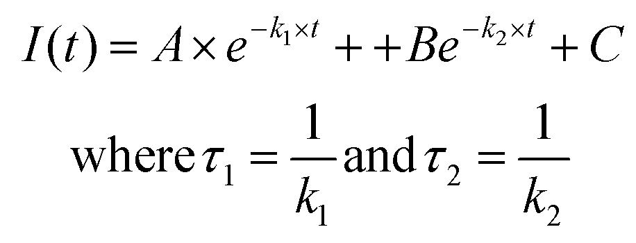
where kRET1 is the non-radiative RET decay rate and khyb1 and kref1 are the fast decay rates of the hybrid and the reference sample, respectively. The hybrid sample here denotes QDs deposited on an AlOx spacer layer with thicknesses of 8 nm and 18 nm. The reference sample has QDs deposited on an AlOx spacer layer with 50 nm thickness. The efficiencies of the RET transfer process from QDs to Si for separation distances of 18 nm and 8 nm are 4.5% and 15%, respectively. The RET efficiency we calculated for the observed process appears to be consistent with previous experimental and theoretical studies on similar materials and separation distances.23,29,30 Therefore, we can conclude that RET participates in our hybrid QD/IBC solar cells. The reason for choosing 18 nm AlOx over 8 nm AlOx in our IBC solar cell was due to better surface passivation. The 18 nm AlOx yielded a minority carrier lifetime of 1.6 ms, which was twice that of passivation from 8 nm AlOx (800 μs). High lifetimes exceeding 6 ms have been demonstrated31 for ultra-thin AlOx films with a thickness of 5 nm. When using such an optimized thin AlOx passivation layer, the hybrid QD IBC solar cell can benefit further from more efficient RET.

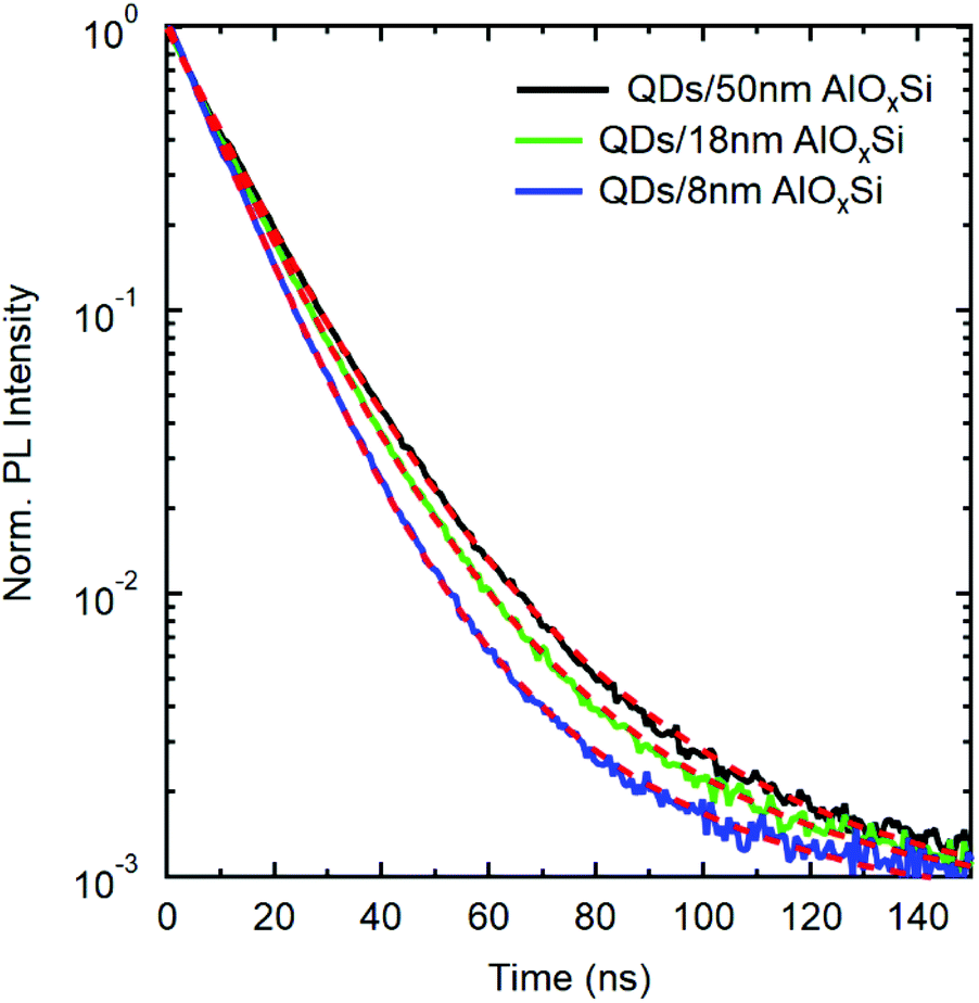 | ||
| Fig. 5 Photoluminescence dynamics of CdSe1−xSx/ZnS (core/shell) QDs deposited on 50 nm AlOx on Si (black solid line), 18 nm AlOx on Si (green solid line), and 8 nm AlOx on Si (red solid line). The red dashed line is the bi-exponential fit. | ||
3. Conclusion
In this work, we demonstrate an efficient hybrid QD/solar cell architecture to boost the performance of the IBC solar cells. The CdSe1−xSx/ZnS QDs absorb shorter wavelength photons and allow their luminescence downshifting to longer wavelength photons, boosting the performance of the IBC solar cell. When the thickness of the QDs layer is optimized, the solar cell also benefits from an anti-reflection coating. For the best QD layer thickness, the IBC solar cell shows 39.5% improvement in Jsc through efficient photon management. The boost is due to a combination of anti-reflection, RET, and LDS from the QD layer. The presence of LDS is confirmed from the enhancement in IQE. The improvement through LDS can be further enhanced using even higher quantum yield QDs. The RET in our hybrid IBC solar cell was demonstrated by varying the distance between QDs and Si. A RET efficiency of 15% can be achieved with an AlOx spacer layer thickness of 8 nm. Using the opto-electronic modelling tool OPAL2,22 based on the measured refractive index data of the CdSe1−xSx/ZnS quantum dots, it was estimated that 17% of the Jsc boost observed can be accounted for from the RET and LDS processes alone. The application of nanostructures to this architecture could alter the directionality of light emission from QDs towards the solar cell, boosting the performance of hybrid IBC solar cell even further.4. Experimental section
Cell fabrication
An N-type double side polished float zone (FZ) Si wafer 〈100〉, 1–5 ohm-cm, 4′′, 280 μm, was used to fabricate the 1 × 1 cm2 IBC solar cells. The fabrication process for the solar cell is described in ref. 32. These wafers did not undergo any pre-oxidation steps to annihilate the bulk defects present in the FZ material. The front surface passivation was formed using atomic layer deposition (ALD) AlOx (18 nm), whilst the rear surface passivation was a stack formed of ALD AlOx (10 nm) and PECVD SiNx![[thin space (1/6-em)]](https://www.rsc.org/images/entities/char_2009.gif) :H (60 nm). Both the emitter and the back-surface field were formed using thermal diffusion with BBr3 and POCl3, respectively. The metal contacts were formed using thermal evaporation of aluminum (0.4 μm). The interdigitation of the diffused areas and the metal contacts (including contact holes) were formed via a 4-stage photolithography process. The busbar is 500 μm wide, the P+ region is 1000 μm wide, the N+ region is 500 μm wide, and the spacing between the interdigitated fingers is 500 μm.
:H (60 nm). Both the emitter and the back-surface field were formed using thermal diffusion with BBr3 and POCl3, respectively. The metal contacts were formed using thermal evaporation of aluminum (0.4 μm). The interdigitation of the diffused areas and the metal contacts (including contact holes) were formed via a 4-stage photolithography process. The busbar is 500 μm wide, the P+ region is 1000 μm wide, the N+ region is 500 μm wide, and the spacing between the interdigitated fingers is 500 μm.
Deposition of QDs
A solution of CdSe1−xSx/ZnS (core/shell) quantum dots with an alkyl ligand surface was procured from Cytodiagnostics (Trilite™ Fluorescent Nanocrystals 525 nm – alkyl). The solution of CdSe1−xSx/ZnS QDs has 1s absorption and emission peaks of 502 nm and 533 nm, respectively. The colloidal QDs in toluene were spun onto the IBC solar cell at a spin speed of 6000 rpm. The concentration of colloidal QDs in toluene was varied to obtain QD layer thicknesses of 6 nm, 30 nm, 64 nm, 71 nm, 83 nm and 96 nm.Optical characterisation
CdSe1−xSx/ZnS QDs were spin-coated onto glass, and absorption spectra were obtained using a Jasco V-570 UV/VIS/NIR spectrophotometer. The effective complex refractive index (n and k) of the QD layer deposited on Si was measured and modelled using a Woollam M-2000 ellipsometer and CompleteEASE software. The CdSe1−xSx/ZnS QD layer on the IBC solar cell was pumped at 400 nm using a coherent chameleon laser, and photoluminescence spectra were obtained using an optical fiber coupled to a BWTEK GlacierX TE cooled CCD spectrometer. The PLQY of QDs was measured in solution using an Otsuka QE-2000 quantum efficiency measurement system.Solar cell characterisation
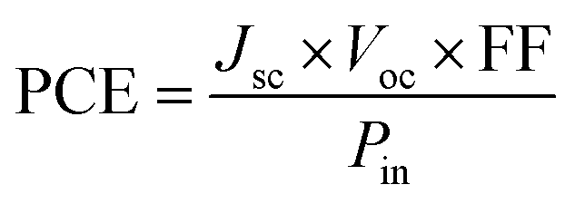
Current density–voltage (J–V) measurements of solar cells were performed using a Sun 3000 solar simulator (ABET Technologies). The solar simulator was equipped with spectral filters to simulate the AM1.5G spectrum. All the I–V measurements were carried out under 1 sun illumination of 100 mW cm−2. The solar simulator was calibrated with a certified reference Si solar cell. The power conversion efficiency (PCE) of the solar cell was determined from the fraction of input power density (Pin) converted to output power and is given by the following relation:where Jsc denotes the short-circuit density and Voc is the open-circuit voltage. The fill factor (FF = (Jm × Vm)/(Jsc × Voc)) denotes the squareness of the J–V curve, where Jm and Vm denote the current density and voltage at the maximum power operating point of the solar cell, respectively. A Bentham PVE 300 photovoltaic system was used to measure the reflectance and external quantum efficiency (EQE) of the solar cell. A monochromated dual xenon/quartz halogen lamp was used as an excitation source, and an integrating sphere equipped with a Si photodiode was used for detection. The solar cell (or reference standard) is placed at the rear reflectance port of the integrating sphere. The reflectance of the solar cell is determined by the ratio of signals (Is/Iref) measured by the Si photodiode, where Is and Iref are the reflectance signal from the solar cell and reference standard, respectively. A diffuse reflectance standard coated with the same material (barium sulphate) as the interior wall of the integrating sphere was used as a reference standard in our reflectance measurements.
Using the same excitation source, the EQE measurement is performed by illuminating the cell with monochromatic light, swept in the wavelength range of 300 nm–1100 nm whilst measuring the short circuit current. From this, the spectral response is determined and then converted to EQE. When measured under light bias conditions, the white light intensity was close to 1 sun. To avoid any discrepancy in the EQE results, the system is calibrated each time before measurement, using a reference Si photodetector. The IQE of the solar cell was determined from the EQE and reflectance (R) of the solar cell and is given by the relation: IQE = EQE/(1 − R). Transmission of light through the cell is assumed to be negligible.
Time-resolved photoluminescence measurement
Thin films of CdSe1−xSx/ZnS QDs deposited by spin coating onto glass and IBC solar cells were optically excited with a pulsed monochromatic laser at a wavelength of 400 nm and a repetition rate of 800 kHz. A titanium:sapphire tunable laser system (Coherent Chameleon Ultra II) was used to generate pulsed laser emission at 800 nm with a repetition rate of 80 MHz that was reduced to 800 kHz with a Spectra-Physics 3980 pulse picker. Finally, a Coherent Harmonic SHG was used to double the fundamental frequency. A series of ND filters were used to control the excitation power at the sample site. Photoluminescence emitted from the sample was then collected in a confocal configuration and filtered with a Bentham M300 single monochromator, before being directed to an Avalanche photodiode coupled to a Becker Hickl SP-140 Time-Correlated Single Photon Counting card, providing an instrument response function (IRF) of about 150 ps. Recorded PL decay curves were analyzed and decay rates were extracted by biexponential fitting using standard chi-square minimization methods.Conflicts of interest
There are no conflicts to declare.References
- International Energy Agency, Solar Photovoltaics, https://www.iea.org/topics/renewables/solar/, (accessed 10 May 2019).
- K. Yoshikawa, W. Yoshida, T. Irie, H. Kawasaki, K. Konishi, H. Ishibashi, T. Asatani, D. Adachi, M. Kanematsu, H. Uzu and K. Yamamoto, Sol. Energy Mater. Sol. Cells, 2017, 173, 37–42 CrossRef CAS.
- D. D. Smith, P. Cousins, S. Westerberg, R. De Jesus-Tabajonda, G. Aniero and Y.-C. Shen, IEEE J. Photovolt., 2014, 4, 1465–1469 Search PubMed.
- E. M. Sanehira, A. R. Marshall, J. A. Christians, S. P. Harvey, P. N. Ciesielski, L. M. Wheeler, P. Schulz, L. Y. Lin, M. C. Beard and J. M. Luther, Sci. Adv., 2017, 3, eaao4204 CrossRef PubMed.
- A. J. Nozik, M. C. Beard, J. M. Luther, M. Law, R. J. Ellingson and J. C. Johnson, Chem. Rev., 2010, 110, 6873–6890 CrossRef CAS PubMed.
- R. J. Ellingson, M. C. Beard, J. C. Johnson, P. Yu, O. I. Micic, A. J. Nozik, A. Shabaev and A. L. Efros, Nano Lett., 2005, 5, 865–871 CrossRef CAS PubMed.
- N. J. L. K. Davis, M. L. Böhm, M. Tabachnyk, F. Wisnivesky-Rocca-Rivarola, T. C. Jellicoe, C. Ducati, B. Ehrler and N. C. Greenham, Nat. Commun., 2015, 6, 8259 CrossRef CAS PubMed.
- NREL, Best Research-cell Efficiencies, https//www.nrel.gov/pv/assets/pdfs/best-research-cell-efficiencies-190416.pdf, (accessed 10 May 2019).
- M. Brossard, C.-Y. Hong, M. Hung, P. Yu, M. D. B. Charlton, P. G. Savvidis and P. G. Lagoudakis, Adv. Opt. Mater., 2015, 3, 263–269 CrossRef CAS.
- C. Krishnan, M. Brossard, K.-Y. Lee, J.-K. Huang, C.-H. Lin, H.-C. Kuo, M. D. B. Charlton and P. G. Lagoudakis, Optica, 2016, 3, 503 CrossRef CAS.
- Y.-K. Liao, M. Brossard, D.-H. Hsieh, T.-N. Lin, M. D. B. Charlton, S.-J. Cheng, C.-H. Chen, J.-L. Shen, L.-T. Cheng, T.-P. Hsieh, F.-I. Lai, S.-Y. Kuo, H.-C. Kuo, P. G. Savvidis and P. G. Lagoudakis, Adv. Energy Mater., 2015, 5, 1401280 CrossRef.
- T. Trupke, M. A. Green and P. Würfel, J. Appl. Phys., 2002, 92, 1668–1674 CrossRef CAS.
- X. Pi, Q. Li, D. Li and D. Yang, Sol. Energy Mater. Sol. Cells, 2011, 95, 2941–2945 CrossRef CAS.
- F. Sgrignuoli, P. Ingenhoven, G. Pucker, V. D. Mihailetchi, E. Froner, Y. Jestin, E. Moser, G. Sànchez and L. Pavesi, Sol. Energy Mater. Sol. Cells, 2015, 132, 267–274 CrossRef CAS.
- K. Yoshikawa, H. Kawasaki, W. Yoshida, T. Irie, K. Konishi, K. Nakano, T. Uto, D. Adachi, M. Kanematsu, H. Uzu and K. Yamamoto, Nat. Energy, 2017, 2, 17032 CrossRef CAS.
- SunPower, MAXEON GEN II Solar Cells, https://us.sunpower.com/sites/default/files/media-library/spec-sheets/sp-sunpower-maxeon-solar-cells-gen2.pdf, (accessed 10 May 2019).
- T. Rahman, R. S. Bonilla, A. Nawabjan, P. R. Wilshaw and S. A. Boden, Sol. Energy Mater. Sol. Cells, 2017, 160, 444–453 CrossRef CAS.
- T. Rahman, M. Navarro-Cía and K. Fobelets, Nanotechnology, 2014, 25, 485202 CrossRef PubMed.
- T. Rahman and S. A. Boden, IEEE J. Photovolt., 2017, 7, 1556–1562 Search PubMed.
- S.-F. Leung, M. Yu, Q. Lin, K. Kwon, K.-L. Ching, L. Gu, K. Yu and Z. Fan, Nano Lett., 2012, 12, 3682–3689 CrossRef CAS PubMed.
- Y. Fu, D. Kim, W. Jiang, W. Yin, T. K. Ahn and H. Chae, RSC Adv., 2017, 7, 40866–40872 RSC.
- K. R. McIntosh and S. C. Baker-Finch, in 2012 38th IEEE Photovoltaic Specialists Conference, IEEE, 2012, pp. 265–271.
- P. Andreakou, M. Brossard, C. Li, P. G. Lagoudakis, M. Bernechea and G. Konstantatos, EPJ Web Conf., 2013, 54, 01017 CrossRef CAS.
- B. Martín-García, P. M. R. Paulo, S. M. B. Costa and M. M. Velázquez, J. Phys. Chem. C, 2013, 117, 14787–14795 CrossRef.
- M. Jones, S. S. Lo and G. D. Scholes, J. Phys. Chem. C, 2009, 113, 18632–18642 CrossRef CAS.
- T. Alejo, P. M. R. Paulo, M. D. Merchán, E. Garcia-Fernandez, S. M. B. Costa and M. M. Velázquez, J. Lumin., 2017, 183, 113–120 CrossRef CAS.
- M. G. Bawendi, P. J. Carroll, W. L. Wilson and L. E. Brus, J. Chem. Phys., 1992, 96, 946–954 CrossRef CAS.
- P. H. Sher, J. M. Smith, P. A. Dalgarno, R. J. Warburton, X. Chen, P. J. Dobson, S. M. Daniels, N. L. Pickett and P. O'Brien, Appl. Phys. Lett., 2008, 92, 101111 CrossRef.
- C. R. Belton, G. Itskos, G. Heliotis, P. N. Stavrinou, P. G. Lagoudakis, J. Lupton, S. Pereira, E. Gu, C. Griffin, B. Guilhabert, I. M. Watson, A. R. Mackintosh, R. A. Pethrick, J. Feldmann, R. Murray, M. D. Dawson and D. D. C. Bradley, J. Phys. D: Appl. Phys., 2008, 41, 094006 CrossRef.
- S. Hoang, A. Ashraf, M. D. Eisaman, D. Nykypanchuk and C.-Y. Nam, Nanoscale, 2016, 8, 5873–5883 RSC.
- G. Dingemans, R. Seguin, P. Engelhart, M. C. M. van de Sanden and W. M. M. Kessels, Phys. Status Solidi RRL, 2010, 4, 10–12 CrossRef CAS.
- T. Rahman, A. To, M. E. Pollard, N. E. Grant, J. Colwell, D. N. Payne, J. D. Murphy, D. M. Bagnall, B. Hoex and S. A. Boden, Prog. Photovolt. Res. Appl., 2018, 26, 38–47 CrossRef CAS.
Footnote |
| † Electronic supplementary information (ESI) available. See DOI: 10.1039/c9nr04003j |
| This journal is © The Royal Society of Chemistry 2019 |