
Silver nanowire inks for direct-write electronic tattoo applications†
Nicholas X.
Williams
 a,
Steven
Noyce
a,
Jorge A.
Cardenas
a,
Matthew
Catenacci
b,
Benjamin J.
Wiley
b and
Aaron D.
Franklin
*ab
a,
Steven
Noyce
a,
Jorge A.
Cardenas
a,
Matthew
Catenacci
b,
Benjamin J.
Wiley
b and
Aaron D.
Franklin
*ab
aDepartment of Electrical and Computer Engineering, Duke University, Durham, NC 27708, USA. E-mail: aaron.franklin@duke.edu; Tel: +1-919-681-9471
bDepartment of Chemistry, Duke University, Durham, NC 27708, USA
First published on 9th July 2019
Abstract
Room-temperature printing of conductive traces has the potential to facilitate the direct writing of electronic tattoos and other medical devices onto biological tissue, such as human skin. However, in order to achieve sufficient electrical performance, the vast majority of conductive inks require biologically harmful post-processing techniques. In addition, most printed conductive traces will degrade with bending stresses that occur from everyday movement. In this work, water-based inks consisting of high aspect ratio silver nanowires are shown to enable the printing of conductive traces at low temperatures and without harmful post-processing. Moreover, the traces produced from these inks retain high electrical performance, even while undergoing up to 50% bending strain and cyclic bending strain over a thousand bending cycles. This ink has a rapid dry time of less than 2 minutes, which is imperative for applications requiring the direct writing of electronics on sensitive surfaces. Demonstrations of conductive traces printed onto soft, nonplanar materials, including an apple and a human finger, highlight the utility of these new silver nanowire inks. These mechanically robust films are ideally suited for printing directly on biological substrates and may find potential applications in the direct-write printing of electronic tattoos and other biomedical devices.
Introduction
Electronic tattoos have garnered recent attention in the biomedical field as a flexible, low-cost approach for creating bio-interfacing electronics.1–4 The numerous publications on this topic range in focus from sensors,5–10 to light emitting diodes,11–13 to transistors.14–16 Many of these reports describe the fabrication of electronic tattoos (also referred to as epidermal electronics),3,4,13,17–20 which are skin-conforming electronic devices. Printed electronics are ideally suited for the fabrication of electronic tattoos due to their compatibility with flexible substrates,21,22 low-cost fabrication,23 and customizability. While structure and materials may vary between devices, electrically conductive inks are a common feature that allow for the creation of intricate electronics. However, a standard requirement for achieving low resistivity films with printable conductive inks is some form of relatively harsh post-processing.Post-processing of printed conductive inks encompasses a range of techniques, including sintering/annealing at elevated temperatures (>70 °C),24–30 rinsing or soaking in hazardous chemicals,31,32 exposure to ultraviolet radiation33,34 or laser sintering.35,36 These harsh conditions preclude printing directly onto the epidermis, which would open the way for significant developments in the area of patient-specific monitoring or treatment with electronics. Thus, nearly all bio-interfacing electronics are completely fabricated on disposable substrates and subsequently transferred to a biological surface. This method, referred to as the transfer method, is less than ideal due to possible inconsistencies in transferring, which could affect device performance, specific location for most sensitive/desired operation, and lifetime. Thus, the development of conductive printable inks that are curable at low temperatures is key to enabling the next generation of biomedical devices in the form of electronic tattoos.
In addition to direct-write printing onto sensitive biological surfaces, seamless incorporation of electronic tattoos also necessitates high levels of flexibility and the ability to withstand the repetitive bending strain caused by everyday movement. Previous reports on low-temperature printed conductive traces demonstrate admirable bending performance.37,38 These represent a crucial development towards realizing a seamless bio-interface with electronics. Zhu et al. demonstrates an ink with a rapid dry time but poor bending performance whereas Russo et al. develops an ink with superior bending performance but required an extended dry time at room temperature in addition to using nanoparticles, which are known to be cytotoxic.37–39 Developing an ink and printing approach that can yield both rapid curing time and optimal bending performance has the potential to create a robust printed electronic tattoo with an extended lifetime. One possible method to create this improved hybrid is the use of high aspect ratio electronic materials as the functional component for an ink. Silver nanowires (AgNW) are a high aspect ratio nanomaterial that have decreased cytotoxicity as compared to AgNPs of the same diameter.40,41 In addition, when interacting with cells as a thin film, AgNWs have an even further reduced cytotoxicity.42 Thus, AgNW inks could be used as a less damaging alternative to AgNPs. Moreover, they have also shown promise for achieving high conductivity printed traces and have been shown to maintain their conductivity when the underlying substrate is bent.43–45 In addition, conductive silver nanowire networks can be created with minimal post-processing at relatively low temperatures (70 °C) with conductivities orders of magnitude higher than silver nanoparticles (AgNP).46 However, biological materials begin to degrade rapidly at temperatures greater than 38–40 °C. Frequently, inks deliver on one of these beneficial properties (low temperature printing and bending performance) at the expense of the other. Thus, an ink capable of a truly seamless interface with a biological substrate must obtain high conductivity when printed at or near room temperature.47
Herein, we demonstrate room-temperature aerosol jet printing of highly conductive traces comprised of silver nanowires, which facilitates the direct-write printing of conductive electrodes onto biological materials, such as the epidermis. Silver nanowires were synthesized and suspended in water with a small amount of hydroxypropyl methylcellulose (HPMC) as a viscosifier. We explored the temperature dependence of the printing on the final printed film's conductivity as well as the importance of silver nanowire length and concentration on the electronic properties of the film. We found that the sheet resistance was dependent on both the printing temperature as well as the ink concentration. Ultimately, we successfully developed an ink that can be printed into conductive traces on sensitive biological surfaces with the traces retaining their electronic performance even under high bending strains of up to 50%.
Experimental
Materials
Silver nanowires were fabricated using the polyol method as described in ref. 48. After rinsing the wires in acetone twice and water once, the wires were suspended in water at the desired concentration. These concentrations ensured ink stability for up to 6 months. The silver nanoparticle ink was purchased from UT Dots Inc. (UT Dots UTDAg40x) and mixed with terpinol at a 9![[thin space (1/6-em)]](https://www.rsc.org/images/entities/char_2009.gif) :1 ratio of ink:terpinol.
:1 ratio of ink:terpinol.
Substrate preparation
All inorganic samples (glass, silicon, and polyimide Kapton) were ultrasonicated in isopropyl alcohol for 5 minutes, rinsed with deionized water, dried with nitrogen, and then ultrasonicated again in acetone and rinsed and dried using the same method. No cleaning or sample preparation was performed on any biological samples.Silver nanowire printing
A 200 μm diameter nozzle was used to print all silver nanowire traces and films. A print speed of 1 mm s−1 was used for all silver nanowire printing. The exact printing parameters varied slightly from print to print to ensure consistent performance. The sheath flow used was 25 SCCM, the atomizer flow rate was 40–50 SCCM, and the ultrasonic inducer current was 340–350 mA.Silver nanoparticle printing
A 150 μm diameter nozzle was used to print all silver nanowire traces and films. A print speed of 3 mm s−1 was used for all silver nanoparticle printing. While the exact printing parameters varied slightly from print to print, in general the sheath flow used was 25 SCCM, the atomizer flow rate was 16 SCCM and the ultrasonic inducer current was 340–350 mA. The silver nanoparticle ink was printed with a platen temperature of 60 °C and annealed in an oven at 200 °C for 1 hour.Instrumentation and characterization
SEM images were taken at the Duke Pathology Lab and film heights were measured using an optical profilometer (Zygo NewView 5000) at the Shared Materials Instrumentation Facility at Duke University. The sheet resistance of the deposited films was measured using a 4-point probe method and a Keithley 2400 source measure unit.Bend tests
The silver nanowire networks, using the 10 mg ml−1 formulation described above, were printed at 20 °C with no additional processing for a total of 3 print passes. The silver nanoparticle inks were printed at 60 °C and annealed at 200 °C for 1 hour with 1 printing pass. A Signatone H100 tabletop probe station connected to an Aglient Technologies B1500A Semiconductor Device Analyzer was used to test the resistance across the device in both bent and unbent states. All tests were performed using a 127 μm thick Kapton substrate. In addition, all bending tests were performed by hand using a dowel of the desired radius as a guide. The repetitive cycling tests were performed by hand, measuring the sheet resistance after a bending cycle was completed. Each test was performed in quadruplicate. Bending strain was calculated using the following formula: ε = D/2R, where ε is bending strain, D is the thickness of the substrate, and R is the bending radius, thus 50% bending strain occurs when the substrate us folded in half.Results and discussion
Silver nanowires were synthesized using the polyol method, as described in a previous publication.48 Both long (average length of 20 μm and an aspect ratio of 180) and short (average length of 4 μm and an aspect ratio of 120) nanowires were suspended in water at 2–3 mg ml−1 and 10 mg ml−1, respectively, to create the inks used in this study. Water was selected as the solvent because of its biocompatibility and relative ease of creating nanowire suspensions. All printing for this work was performed using an Optomec Aerosol Jet 300 printer. An image and cross-sectional schematic representation of the printer head and nozzle can be found in Fig. 1a. Aerosol jet printing is the ideal deposition method for the printing of high aspect ratio materials, such as silver nanowires, as this method relies on a protective, annular sheath flow which surrounds the ink as it is being carried through the deposition nozzle. This sheath flow facilitates ink transportation to the substrate surface, concentrating the ink stream into a dense network with a small spot size and preventing the ink from contacting the deposition head – an issue that has been previously reported to lead to nozzle clogging after only short printing durations in the inkjet printing of silver nanowires.47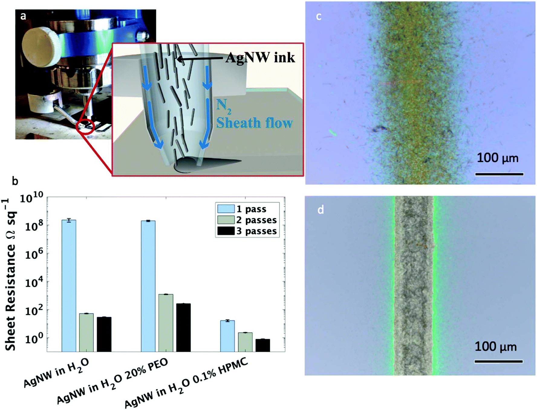 | ||
| Fig. 1 Printing of silver nanowire traces. (a) Aerosol jet printer head and cross-sectional schematic representation of printer nozzle. (b) Sheet resistance values for silver nanowire films at 1, 2, and 3 print passes with various viscosity modifiers printed on glass. Error bars indicate one standard deviation as measured over 6 separate prints. (c) Optical image of a printed silver nanowire trace with no additives or modifiers printed on glass. (d) Optical image of a printed silver nanowire trace with the addition of 0.1% w/w HPMC printed on glass. | ||
Initial attempts at printing the nanowire inks without additives onto a glass slide created traces with undesirably high sheet resistance (Fig. 1b). This was caused by a the ink spreading on the substrate due to the high surface energy of the glass substrate,49 resulting in a diffuse line with a relatively wide linewidth of approximately 150 μm (Fig. 1c). The current path in silver nanowire traces moves through a percolation network (i.e., from one nanowire to the next nanowire and so forth); thus, the sheet resistance of a nanowire film is largely dependent on the number of conduction pathways. Increasing the film density will increase number of conduction pathways, which will decrease current crowding and reduce the resulting film's resistivity. As indicated by the image of the printed line (Fig. 1d) and sheet resistance (Fig. 1b), respectively, the diffusivity of the print necessitated the addition of a viscosity-modifying additive to increase the line quality, and thus, the AgNW density. Two different additives were explored, both of which were chosen due to their low cost and relative biocompatibility. Ethylene glycol at a concentration of 20% v/v was used successfully in previous publications describing silver nanowires suspended in isopropyl alcohol.46 However, in this water-based ink, the same percentage addition of ethylene glycol was found to have a negative impact on the printed sheet resistance after 1, 2, and 3 printing passes when compared to silver nanowires in water alone. In water, the addition of the large volume of an insulating polymer leaves a non-conductive residue on the deposition that can block current propagation (Fig. S1†). In contrast, the addition of only 0.1 mg ml−1 HPMC decreased the sheet resistance by 7 orders of magnitude with one printing pass (Fig. 1b). A corresponding decrease in sheet resistance was observed regardless of the substrate, where nearly identical sheet resistance values were observed with both silicon and glass substrates. In addition, the line quality was greatly improved (Fig. 1d), with an average line width of less than 80 μm and a significantly reduced line edge roughness with almost no overspray. All subsequent tests were performed with the addition of 0.1 mg ml−1 HPMC to the water-based ink.
The electrical properties of the nanowire traces were characterized by measuring the sheet resistance of films created with 1, 2, and 3 printer passes (an image of these films is shown in Fig. 2a). Testing both the short and long nanowire inks at a range of concentrations (from 0.5 mg ml−1 to their settling concentrations of 3 mg ml−1 and 10 mg ml−1 for long and short nanowires, respectively) indicated that the main factor contributing to the reduction of sheet resistance at these aspect ratios is the ink concentration (Fig. 2b and c), rather than the nanowire length. There were diminishing improvements to the electrical properties when increasing ink concentration greater than 5 mg ml−1; thus, for clarity we only plotted ink concentrations below 5 mg ml−1. Film thickness values and an SEM image of the printed nanowire traces can be found in Fig. S2 and S3,† respectively. As can be seen, at the same ink concentration, the short nanowires produce a slightly denser film, which may explain the small decrease in sheet resistance observed when short and long nanowires are printed at the same concentration.
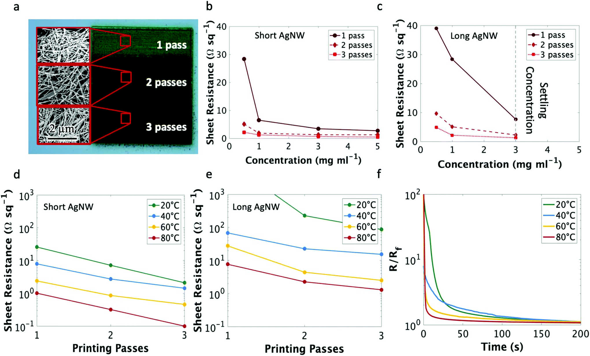 | ||
| Fig. 2 Characterization of printed silver nanowire films with 0.1% w/w HPMC. (a) Photograph of printed silver nanowire square with regions of 1, 2, and 3 print passes printed onto glass. Sheet resistance values comparing short (average length 4 μm and an aspect ratio of 120) (b) and long (average length 20 μm and an aspect ratio of 180) (c) silver nanowire inks at increasing printing passes (1 pass – solid, 2 passes – large dash, 3 passes – small dash) as a function of ink concentration (printed at 80 °C) (d) Sheet resistance of short silver nanowire films (printed at 10 mg ml−1) at different platen temperatures as a function of printing passes. (e) Sheet resistance of long silver nanowire films (printed at 2 mg ml−1) at different platen temperatures as a function of printing passes. (f) Change in resistance for printed short silver nanowire traces at different platen temperatures over time to demonstrate the effect of ink drying time. | ||
Subsequently, the electrical properties of the printed films were characterized for the short nanowires with varying printer platen temperature (Fig. 2d). As expected, the sheet resistance decreased with increasing printer platen temperature, reaching a minimum of 0.13 Ω sq−1 with 3 passes of the short nanowires at 80 °C, as compared to commercial aerosol jet printed silver nanoparticle ink (UTDots Inc., Ag40X), which achieved a sheet resistance of 0.22 Ω sq−1 after annealing at 200 °C. The temperature dependence of the AgNW sheet resistance is largely due to the evaporation rate of the solvent at different substrate temperatures. An increased atomization flow rate, and thus higher ink deposition rate, is possible at elevated temperatures because the ink solvent evaporates rapidly enough to maintain adequate line quality. Were the same high atomizer flow rates of the elevated temperature prints attempted at a lower substrate temperature, the ink would not evaporate fast enough to prevent spill over from buildup of liquid ink at a specific location (Fig. S4† provides an image illustrating this phenomenon). This would, in turn, decrease the nanowire density and thus increase the sheet resistance. Hence, to maintain ideal line quality (and thus nanowire density) the atomization flow rate must be modulated with temperature. Even so, low resistances were achieved with 3 passes of the nanowire ink at all printing temperatures and single digit sheet resistances were observed at room temperature with the short nanowires. These sheet resistance values are on par with other low-temperature printable conductive inks that required elevated temperature26,29 or chemical annealing post-processing.50 The same temperature trend was observed with the long nanowires (Fig. 2e); however, the long nanowires could not be suspended at a concentration higher than 3 mg ml−1.
In addition to sufficiently low resistivity, a direct-printed electronic tattoo must have a rapid curing time to ensure functionality, as it would be unreasonable for a patient to wait hours before a device is capable of conducting current. To test drying time, a silver nanowire trace was printed to connect two conductive pads and the electrical resistance was measured as a function of time. The results are shown in Fig. 2f. At room temperature, the traces achieved a resistance within 5% of the final resistance less than 2 minutes after printing. This high resistance duration decreased with increasing platen temperature as the solvent evaporation rate was increased.
Addressing the need to withstand repetitive bending strain caused by wearer movement, Fig. 3 explores the bending properties of the conductive traces created with the printed nanowire inks. Silver nanoparticles were selected as a comparative ink as they are the most frequently used ink for printing conductive traces. The nanowire films did not experience any noticeable change in electrical performance until undergoing a bending radius of less than 5 mm (depicted in Fig. 3a) and saw only a 7.2 ± 0.3% increase in sheet resistance on average when the underlying substrate was folded in half and creased (as can be observed in the inset of Fig. 3a). This is two orders of magnitude lower than the change in sheet resistance when silver nanoparticle traces are bent (Fig. S5†). In addition, the increase in resistance with the nanowire films was reversible for all bending radii (Fig. S6† shows the resistance change with 6 consecutive bending cycles at a bend radius of 0.1 mm).
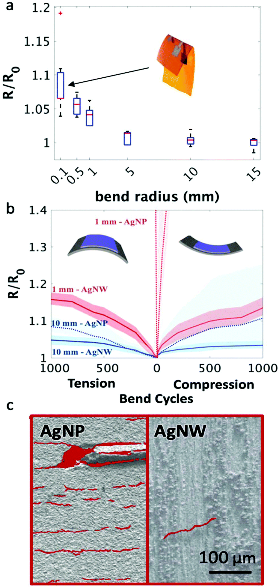 | ||
| Fig. 3 Physical bending properties of printed silver NW traces on Kapton. (a) Change in resistance of printed silver nanowire trace as a function of bending radius – measurements taken while substrate was bent. The median is marked with a red line. The first and third quartiles are demarcated by the blue box and the whiskers extend to the furthest data points not considered outliers. The red crosses note the outliers. (b) Resistance degradation under cyclic bending of silver nanowire (solid lines) and silver nanoparticle (dashed lines) traces where the shaded regions are the standard deviation at a bending radius of 10 mm (blue) and 1 mm (red) up to 1000 bending cycles in both tensile bending strain and compressive bending strain. (c) SEM images of silver nanoparticle (left) and silver nanowire (right) traces after 100 bending cycles (silver nanoparticle) and 1000 bending cycles (silver nanowire). Cracks in the print are highlighted in red. | ||
Cyclic bend tests on both nanowire and nanoparticle printed films were performed to test integrity under repetitive bending. The nanowire films performed significantly better than the nanoparticles under both tensile and compressive bending strain at small and large bending radii (Fig. 3b). After 1000 bending cycles at a 10 mm bend radius, the nanowire films reached a maximum sheet resistance only 5.7 ± 1.6% higher than baseline on average for both tension and compression bending cycles, whereas the nanoparticle films had on average a 9 ± 1.1% and 11 ± 3.2% increase in sheet resistance for tension and compression, respectively. The differences are enhanced further with a smaller 1 mm bending radius. After 50–100 cycles, the nanoparticle films became insulating, whereas the nanowires saw an average 15.0 ± 1.7% and 13.4 ± 2.4% increase in sheet resistance after 1000 bending cycles in compression and tension, respectively. Fig. 3c illustrates the cause of this difference in resilience to bending degradation with SEM images taken from the nanoparticle films after 100 bending cycles at a 1 mm bend radius and the nanowire films after 1000 bending cycles at a 1 mm bend radius (Fig. S7† depicts the SEM images both with and without the highlights). After 100 bend cycles, the nanoparticle films were suffused with cracks over the entirety of the film, with a crack density of 1100 cracks μm−2 while after 1000 bend cycles at a 1 mm bend radius, the nanowire films only had a single crack over an area of 1 mm by 5 mm, which was the entire printed area. The increase in bending resilience when compared to nanoparticle films, in terms of both the limited resistance degradation and the decrease in crack density, can be attributed to the high-aspect ratio of the nanowires, which allow for maintained current pathway even when the substrate is bent, and the low-temperature print, which allows the nanowires behave as individual units and move relative to one another.51
Printing these malleable, conductive traces at room temperature and with rapid dry times allows for direct writing on biological surfaces. Fig. 4a illustrates the printing of a conductive trace on a highly curved and delicate surface, in this case an apple. To test conductivity, nanowire traces also were printed on an oak leaf obtained from a tree outside the lab. As indicated in Fig. 4b, the sheet resistance of the films printed with a single pass on the leaf at 20 and 40 °C were both higher than the those printed on glass; yet, after 2 or more passes, the films had comparable sheet resistances regardless of the substrate. This high sheet resistance is believed to be due to the uneven surface of the leaf in conjunction with the its hydrophobic nature; combined, these caused the printed traces to dry non-continuously, leading to high sheet resistance. With two or more print passes, the printed traces formed a continuous line and the sheet resistance was improved. Even still, single digit sheet resistances were achieved on a biological material substrate, which is competitive with other silver inks printed at room temperature.37,38 This allowed for the functional demonstration of illuminating a light emitting diode (LED) on an apple using nanowire traces (Fig. 4c) as well as the direct deposition of conductive traces onto a finger (Fig. 4d – inset shows LED in the off state). Movie S1† shows a portion of the printing process directly onto the finger. The print on human skin resulted in a sheet resistance of 0.84 Ω sq−1 measured over the length of the 20 mm long trace. The average resistance for clean, dry skin is on the order of 10000 Ω, and wet or broken skin has a resistance of over 1000 Ω,52 thus nearly all current should pass through the conductive trace and the current passing through the skin should be well below the pierceable current threshold.53 It should be noted that the direct-write printing on the finger produced a slightly blurry trace whereas the deposition on the apple produced a trace with a distinct line edge. This is a result of the aqueous nature of the ink, the non-planar surface of the finger, and the grooves from the finger print. Combined, these three factors allowed the ink to flow slightly more than on the apple (which does not have the same grooved structure as the finger). That said, even with the decrease in line resolution, the conductive electronic traces printed directly on a finger were able to operate as distinct electrical connections, as demonstrated by using them to illuminate an LED. The high stability of the silver nanowire films on a bending substrate allowed for continual illumination of the LED even when the finger on which the trace was printed was bent, which can be seen in Fig. 4e (video of bending can be seen in Movie S2†).
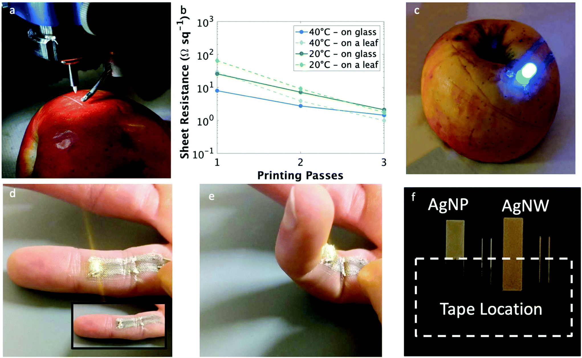 | ||
| Fig. 4 Printed electronic tattoos of conductive traces. (a) Aerosol jet printing of a conductive trace on a curved biological substrate (apple). (b) Sheet resistance of printed traces on inorganic (solid line, glass) and biological (dashed line, leaf) substrates at 20 °C (green) and 40 °C (blue) at 1, 2, and 3 printing passes. (c) Printed conductive circuit on an apple lighting up an LED. (d) Conductive traces were printed on a finger and used to deliver power to an LED, which maintains illumination when the finger is bent (e) – see ESI† video for demonstration. (f) Scotch tape adhesion test comparing the adhesion between a printed film of silver nanoparticles and silver nanowires, where the nanowires are significantly better adhered to the glass substrate. | ||
Another factor not mentioned to this point, though just as critical to making these results possible, is the high adhesion strength of the nanowire traces to the substrates. After applying and removing Scotch tape from the surface, there was no change in sheet resistance for the nanowire film, whereas the nanoparticles were completely removed (Fig. 4f). Sintering the nanoparticles creates a monolithic film; however, due to this bonding between the nanoparticles as well as the strong adhesive of the Scotch tape, the nanoparticle film is entirely removed from the substrate. In contrast, the nanowires are not sintered and thus each nanowire can move independently. Each Scotch tape peel removes the topmost layer of nanowires. At first, the impact is negligible, but after successive tape peels, the resistance begins to increase as fewer nanowires are left to conduct current (Fig. S8†). Based on this effect, printed AgNW electronic tattoos can be removed from the skin with vigorous scrubbing with soap and water for 5 minutes.
To benchmark the performance of the silver nanowire ink formulated in this study as compared with other inks reported in the relevant literature, we have assembled a table of low-temperature silver nanostructured conductive inks in Table 1. As seen from the presented data, the nanowire traces printed in this work demonstrate the highest bending performance as well as the shortest drying/curing time. The resistivity of this ink is on par, if not slightly higher than, other room temperature printed inks; however, the dry time is 60% lower than the next best previous reported,37 the change in resistance at 50% strain is 5% lower,26 and the resistance to cyclic bending degradation is 15% better.38 Achieving record performance in one of these categories can often be realized at the cost of the other. For example, the report with the next lowest change in resistance at 50% strain required a curing temperature of 150 °C, whereas the ink in this work was cured at room temperature. Of note is that our ink is delivering on all of these performance metrics simultaneously. Ultimately, the ink of choice will require all of these characteristics, rapid curing time without post processing.
| Ink type | Deposition | Substrate | Curing temp. (°C) | Curing time | Resistivity (Ω cm) | ΔR/R @ 50% bending strain | ΔR/R @ 1000 bend cycles | Ref. |
|---|---|---|---|---|---|---|---|---|
| AgNW | Aerosol jet | Kapton | 80 | 2 min | 6.9 × 10⁻⁵ | — | — | This work |
| AgNW | Aerosol jet | Kapton | 20 | 2 min | 8.4 × 10⁻⁴ | 1.07 | 1.15 @ 1.0 mm (5% strain) | This work |
| AgNW | Screenprint | PET/glass | 150 | 15 min | 2.1 × 10⁻⁵ | 1.13 | — | 26 |
| AgNP-eInGa | Inkjet | Transfer paper | 60 | 45 min | 2.8 × 10⁻⁵ | 1.48 | — | 54 |
| Ag micro flakes | 3D print | Artificial skin | 20 | 5 min | 7.2 × 10⁻³ | >1.5 | — | 37 |
| AgNP | Pen | Paper | 25 | 30 min | 2.0 × 10⁻⁴ | — | 1.36 @ 1.6 mm (1.5% strain) | 38 |
| AgNP | 3D print | Kapton | 150 | 24 hours | 1.0 × 10⁻³ | 2.95 | 2 @ 5.0 mm (1% strain) | 55 |
| AgNP | Inkjet | Kapton | 150 | 1 hour | 1.5 × 10⁻¹ | 4 | 1.15 @ 2.5 mm (2% strain) | 56 |
| Bulk silver | — | — | — | — | 1.6 × 10⁻⁶ | — | — | — |
Conclusions
In conclusion, we developed a silver nanowire-based biocompatible ink that enables the direct-write printing of conductive traces on biological substrates at room temperature. This ink has a short drying period, which facilitates use within minutes of printing. In addition, low-temperature printing of the nanowires allows for optimal bending performance. Compared to traditional silver nanoparticle inks, this nanowire ink provides low temperature curing, improved bending performance, and greater adhesion to the substrate. Compatibility with sensitive biological surfaces was demonstrated by printing conductive traces directly onto an apple, leaf, and a human finger; in all instances, the ink yielded a robust film with stable conductivity even through significant bending tests. Through incorporation with biocompatible integrated circuits, this ink could assist with the expansion of the wearable electronics industry via directly printed electronic tattoos, enabling ever more useful and complex bio-related sensors, diagnostics, and trackers.Conflicts of interest
There are no conflicts to declare.Acknowledgements
This work was supported by the Department of Defense Congressionally Directed Medical Research Program (CDMRP) under award number W81XWH-17-2-0045 and by the National Institutes of Health (NIH) under award number 1R21HL141028. This work was performed in part at the Duke University Shared Materials Instrumentation Facility (SMIF), a member of the North Carolina Research Triangle Nanotechnology Network (RTNN), which is supported by the National Science Foundation (Grant ECCS-1542015) as part of the National Nanotechnology Coordinated Infrastructure (NNCI).References
- S. R. Krishnan, C. Su, Z. Xie, M. Patel, S. R. Madhvapathy, Y. Xu, J. Freudman, B. Ng, S. Y. Heo, H. Wang, T. R. Ray, J. Leshock, I. Stankiewicz, X. Feng, Y. Huang, P. Gutruf and J. A. Rogers, Small, 2018, 1803192, 1–13 Search PubMed.
- Y. Qiao, Y. Wang, H. Tian, M. Li, J. Jian, Y. Wei, Y. Tian, D. Y. Wang, Y. Pang, X. Geng, X. Wang, Y. Zhao, H. Wang, N. Deng, M. Jian, Y. Zhang, R. Liang, Y. Yang and T. L. Ren, ACS Nano, 2018, 12, 8839–8846 CrossRef CAS PubMed.
- G. S. Cañón Bermúdez, D. D. Karnaushenko, D. Karnaushenko, A. Lebanov, L. Bischoff, M. Kaltenbrunner, J. Fassbender, O. G. Schmidt and D. Makarov, Sci. Adv., 2018, 4, 1–10 Search PubMed.
- Z. Zhan, R. Lin, V.-T. Tran, J. An, Y. Wei, H. Du, T. Tran and W. Lu, ACS Appl. Mater. Interfaces, 2017, 9, 37921–37928 CrossRef CAS.
- M. Zirkl, A. Sawatdee, U. Helbig, M. Krause, G. Scheipl, E. Kraker, P. A. Ersman, D. Nilsson, D. Platt, P. Bodö, S. Bauer, G. Domann and B. Stadlober, Adv. Mater., 2011, 23, 2069–2074 CrossRef CAS.
- N. Shoaie, M. Forouzandeh and K. Omidfar, IEEE Sens. J., 2017, 18, 1835–1843 Search PubMed.
- L. Pan, A. Chortos, G. Yu, Y. Wang, S. Isaacson, R. Allen, Y. Shi, R. Dauskardt and Z. Bao, Nat. Commun., 2014, 5, 1–8 Search PubMed.
- M. Adib, R. Eckstein, G. Hernandez-sosa, M. Sommer and U. Lemmer, IEEE Sens. J., 2018, 18, 494–500 CAS.
- S. Cinti, V. Mazzaracchio, I. Cacciotti, D. Moscone and F. Arduini, Sensors, 2017, 17, 2267 CrossRef.
- Y. Khan, M. Garg, Q. Gui, M. Schadt, A. Gaikwad, D. Han, N. A. D. Yamamoto, P. Hart, R. Welte, W. Wilson, S. Czarnecki, M. Poliks, Z. Jin, K. Ghose, F. Egitto, J. Turner and A. C. Arias, Adv. Funct. Mater., 2016, 26, 8764–8775 CrossRef CAS.
- D. Han, Y. Khan, J. Ting, S. M. King, N. Yaacobi-Gross, M. J. Humphries, C. J. Newsome and A. C. Arias, Adv. Mater., 2017, 29, 1–8 CrossRef.
- V. Wood, M. J. Panzer, J. Chen, M. S. Bradley, J. E. Halpert, M. C. Bawendi and V. Bulović, Adv. Mater., 2009, 9–11 Search PubMed.
- M. K. Choi, J. Yang, K. Kang, D. C. Kim, C. Choi, C. Park, S. J. Kim, S. I. Chae, T. H. Kim, J. H. Kim, T. Hyeon and D. H. Kim, Nat. Commun., 2015, 6, 1–8 Search PubMed.
- M. Ha, J. W. T. Seo, P. L. Prabhumirashi, W. Zhang, M. L. Geier, M. J. Renn, C. H. Kim, M. C. Hersam and C. D. Frisbie, Nano Lett., 2013, 13, 954–960 CrossRef CAS.
- C. Cao, J. B. Andrews and A. D. Franklin, Adv. Electron. Mater., 2017, 3, 1–10 CrossRef.
- T.-Y. Kim, J. Ha, K. Cho, J. Pak, J. Seo, J. Park, J.-K. Kim, S. Chung, Y. Hong and T. Lee, ACS Nano, 2017, 11, 10273–10280 CrossRef CAS.
- N. Karim, S. Afroj, A. Malandraki, S. Butterworth, C. Beach, M. Rigout, K. Novoselov, A. J. Casson and S. Yeates, J. Mater. Chem. C, 2017, 5, 11640–11648 RSC.
- Y. Wang, Y. Qiu, S. K. Ameri, H. Jang, Z. Dai, Y. Huang and N. Lu, npj Flex. Electron., 2018, 2, 6 CrossRef.
- G. E. Bonacchini, C. Bossio, F. Greco, V. Mattoli, Y. Kim, G. Lanzani and M. Caironi, Adv. Mater., 2018, 1706091, 1–8 Search PubMed.
- H. Keum, M. Mccormick, P. Liu, Y. Zhang and F. G. Omenetto, Science, 2011, 333, 838–844 CrossRef.
- B. Chen, M. Kruse, B. Xu, R. Tutika, W. Zheng, M. D. Bartlett, Y. Wu and J. C. Claussen, Nanoscale, 2019, 11, 5222–5230 RSC.
- K. H. Choi, J. T. Yoo, C. K. Lee and S. Y. Lee, Energy Environ. Sci., 2016, 9, 2812–2821 RSC.
- Z. Zhan, J. An, Y. Wei, V. T. Tran and H. Du, Nanoscale, 2017, 9, 965–993 RSC.
- B. Seong, H. Lee, J. Lee, L. Lin, H.-S. Jang and D. Byun, ACS Appl. Mater. Interfaces, 2018, 10, 25666–25672 CrossRef CAS.
- Y. D. Han, S. M. Zhang, H. Y. Jing, J. Wei, F. H. Bu, L. Zhao, X. Q. Lv and L. Y. Xu, Nanotechnology, 2018, 29, 135301 CrossRef CAS PubMed.
- J. Liang, K. Tong and Q. Pei, Adv. Mater., 2016, 28, 5986–5996 CrossRef CAS.
- J. A. Hondred, L. R. Stromberg, C. L. Mosher and J. C. Claussen, ACS Nano, 2017, 11, 9836–9845 CrossRef CAS.
- M. Don, S. Lakshad, J. Kim and J. Lee, Carbon N. Y., 2017, 125, 9–19 CrossRef.
- N. Matsuhisa, D. Inoue, P. Zalar, H. Jin, Y. Matsuba, A. Itoh, T. Yokota, D. Hashizume and T. Someya, Nat. Mater., 2017, 16, 834–840 CrossRef CAS.
- J. A. Cardenas, S. Upshaw, N. X. Williams, M. J. Catenacci, B. J. Wiley and A. D. Franklin, Adv. Funct. Mater., 2019, 29, 1–7 CrossRef.
- A. Shimoni, S. Azoubel and S. Magdassi, Nanoscale, 2014, 6, 11084–11089 RSC.
- Y. K. Lee, J. Kim, Y. Kim, J. W. Kwak, Y. Yoon and J. A. Rogers, Adv. Mater., 2017, 1702665, 1702665 CrossRef.
- S. Lin, X. Bai, H. Wang, H. Wang, J. Song, K. Huang, C. Wang, N. Wang, B. Li, M. Lei and H. Wu, Adv. Mater., 2017, 1703238, 1703238 CrossRef.
- H. Ning, Y. Zhou, Z. Fang, R. Yao, R. Tao, J. Chen, W. Cai, Z. Zhu, C. Yang, J. Wei, L. Wang and J. Peng, Nanoscale Res. Lett., 2017, 12, 546 CrossRef.
- X. Chen, X. Wu, S. Shao, J. Zhuang, L. Xie, S. Nie, W. Su, Z. Chen and Z. Cui, Sci. Rep., 2017, 7, 13239 CrossRef.
- A. J. Kell, C. Paquet, O. Mozenson, I. Djavani-Tabrizi, B. Deore, X. Liu, G. P. Lopinski, R. James, K. Hettak, J. Shaker, A. Momciu, J. Ferrigno, O. Ferrand, J. X. Hu, S. Lafrenière and P. R. L. Malenfant, ACS Appl. Mater. Interfaces, 2017, 9, 17226–17237 CrossRef CAS PubMed.
- Z. Zhu, S.-Z. Guo, T. Hirdler, C. Eide, X. Fan, J. Tolar and M. C. McAlpine, Adv. Mater., 2018, 1707495, 1707495 CrossRef.
- A. Russo, B. Y. Ahn, J. J. Adams, E. B. Duoss, J. T. Bernhard and J. A. Lewis, Adv. Mater., 2011, 23, 3426–3430 CrossRef CAS.
- M. V. Park, A. M. Neigh, J. P. Vermeulen, L. J. J. de la Fonteyne, H. W. Verharen, J. J. Briedé, H. van Loveren and W. H. de Jong, Biomaterials, 2011, 32, 9810–9817 CrossRef CAS.
- M. J. Kim and S. Shin, Food Chem. Toxicol., 2014, 67, 80–86 CrossRef CAS.
- E. K. Sohn, S. A. Johari, T. G. Kim, J. K. Kim, E. Kim, J. H. Lee, Y. S. Chung and I. J. Yu, BioMed Res. Int., 2015, 2015, 1–12 Search PubMed.
- Y. Volkov, J. Coleman, P. E. Lyons, D. Kelleher, N. K. Verma, M. P. O'Sullivan, J. Conroy and H. Kornfeld, Toxicol. Appl. Pharmacol., 2012, 264, 451–461 CrossRef.
- J. Li, Y. Tao, S. Chen, H. Li, P. Chen, M. Z. Wei, H. Wang, K. Li, M. Mazzeo and Y. Duan, Sci. Rep., 2017, 7, 1–9 CrossRef.
- J. H. Seo, I. Hwang, H. D. Um, S. Lee, K. Lee, J. Park, H. Shin, T. H. Kwon, S. J. Kang and K. Seo, Adv. Mater., 2017, 29, 1–8 Search PubMed.
- C. Hwang, W. J. Song, J. G. Han, S. Bae, G. Song, N. S. Choi, S. Park and H. K. Song, Adv. Mater., 2018, 30, 1–8 Search PubMed.
- J. A. Cardenas, M. J. Catenacci, J. B. Andrews, N. X. Williams, B. J. Wiley and A. D. Franklin, ACS Appl. Nano Mater., 2018, 1, 1863–1869 CrossRef CAS.
- D. J. Finn, M. Lotya and J. N. Coleman, ACS Appl. Mater. Interfaces, 2015, 7, 9254–9261 CrossRef CAS.
- I. E. Stewart, M. J. Kim and B. J. Wiley, ACS Appl. Mater. Interfaces, 2017, 9, 1870–1876 CrossRef CAS.
- A. M. J. Van Den Berg, A. W. M. De Laat, P. J. Smith and U. S. Schubert, J. Mater. Chem., 2007, 17, 677–683 RSC.
- X. Yang, M. Sun, Y. Bian and X. He, Adv. Funct. Mater., 2018, 1807615, 1807615 Search PubMed.
- G. W. Huang, H. M. Xiao and S. Y. Fu, Nanoscale, 2014, 6, 8495–8502 RSC.
- R. M. Fish and L. A. Geddes, Plasty, 2009, 9, 407–421 Search PubMed.
- J. Sandby-Møller, T. Poulsen and H. C. Wulf, Acta Derm.-Venereol., 2003, 83, 410–413 Search PubMed.
- M. Tavakoli, M. H. Malakooti, H. Paisana, Y. Ohm, D. G. Marques, P. A. Lopes, A. P. Piedade, A. T. de Almeida and C. Majidi, Adv. Mater., 2018, 30, 1801852 CrossRef.
- B. Y. Ahn, E. B. Duoss, M. J. Motala, X. Guo, S.-I. Park, Y. Xiong, J. Yoon, R. G. Nuzzo, J. A. Rogers and J. A. Lewis, Science, 2009, 323, 1590–1593 CrossRef CAS.
- T. T. Nge, M. Nogi and K. Suganuma, J. Mater. Chem. C, 2013, 1, 5235–5243 RSC.
Footnote |
| † Electronic supplementary information (ESI) available. See DOI: 10.1039/c9nr03378e |
| This journal is © The Royal Society of Chemistry 2019 |