
 Open Access Article
 This Open Access Article is licensed under a Creative Commons Attribution-Non Commercial 3.0 Unported Licence
Identification of a Nitrogen-related acceptor in ZnO nanowires
Jan E.
Stehr
 *a,
Shula L.
Chen
a,
Weimin M.
Chen
a,
Li
Cai
b,
Shaohua
Shen
b and
Irina A.
Buyanova
*a
*a,
Shula L.
Chen
a,
Weimin M.
Chen
a,
Li
Cai
b,
Shaohua
Shen
b and
Irina A.
Buyanova
*a
aDepartment of Physics, Chemistry and Biology, Linköping University, 58183 Linköping, Sweden. E-mail: jan.eric.stehr@liu.se; iribu@ifm.liu.se
bInternational Research Center for Renewable Energy, State Key Laboratory of Multiphase Flow in Power Engineering, Xi'an Jiaotong University, 710049 Shaanxi, China
First published on 15th May 2019
Abstract
Nanostructured ZnO, such as ZnO nanowires (NWs), is a promising material system for a wide range of electronic applications ranging from light emission to water splitting. Utilization of ZnO requires development of effective and controllable p-type doping. Nitrogen is considered among key p-type dopants though the exact origin of N-induced acceptors is not fully understood, especially in the case of nanostructured ZnO. In this work we employ electron paramagnetic resonance (EPR) spectroscopy to characterize N-related acceptors in ZnO NWs. N doping was achieved using ion implantation commonly employed for these purposes. We show that the Fermi level position is lowered in the N implanted NWs, indicating the formation of compensating acceptors. The formed acceptor is unambiguously proven to involve an N atom based on a resolved hyperfine interaction with a 14N nucleus with a nuclear spin I = 1. The revealed center is shown to act as a deep acceptor with an energy level located at about 1.1 eV above the top of the valence band. This work represents the first unambiguous identification of acceptors deliberately introduced in ZnO nanostructures. It also shows that the configuration and electronic structure of the N-related acceptors in nanostructures differ from those in ZnO bulk and thin-films. The present findings are of importance for understanding the electronic properties of nanostructured ZnO required for its future electronic applications.
One-dimensional ZnO nanowire (NW) structures have recently aroused substantial scientific and technological interest as they combine the attractive material properties of ZnO, namely its wide and direct band gap (∼3.3 eV at room temperature) and a large exciton binding energy (60 meV at room temperature), with those of nanoscale objects, including a high surface-to-volume ratio, the freedom to design axial and lateral heterostructures, light trapping, reduced material consumption, etc. In addition, ZnO is nontoxic, sustainable and cheap. Therefore, nanostructured ZnO is considered promising for a wide range of optoelectronic and photonic applications.1–8 In addition, it has emerged as one of the leading material candidates for photocatalytic wastewater purification9 and photocatalytic water splitting.10 Most of the applications require reliable and reproducible acceptor doping. For example, it was demonstrated that the incorporation of deep acceptors increases the photocatalytic efficiency of nanostructured ZnO and lowers operational excitation energies from the ultraviolet into the visible spectral range.9,11–15 P-type doping with shallow acceptors is also an essential requirement for photonic and electronic devices utilizing p–n junctions. Unfortunately, ZnO suffers from the asymmetric doping problem16–18 and fabrication of the p-type material remains a formidable challenge. This hinders wide-spread applications of ZnO. To address this issue, intense research efforts have been undertaken in recent years, evaluating dopants including group-V elements8,19–27 and group-I elements28 as acceptors.
N is considered among the key acceptor dopants, since it has a similar atomic radius and electronegativity to O.29 In view of these merits, N-doping has been used by many groups in order to fabricate p-type ZnO films, though only a limited number of groups was successful in this matter.19–21,30 The difficulty likely stems from both compensating effects of donor-type defects and the low solubility of p-type dopants.31 It is also important to keep in mind that the doping process can be largely affected by growth conditions and the presence of residual defects and impurities. For instance, theoretical and experimental studies have shown that in bulk ZnO nitrogen substituting for oxygen (NO) forms a deep acceptor state.32–34 The energy level of the N acceptor, however, can be affected by its local surrounding,35 complexing with residual group III impurities36 and intrinsic defects,37–39 as well as formation of N–N molecules.40,41 Moreover, it was also suggested that the proximity to the surface lowers the formation energies of the N-related acceptors and modifies their photoionization processes.42–44 This may be partly responsible for the promoted p-type conductivity in nanostructured ZnO,21,28,40,45 though the exact physical mechanism responsible for this effect, as well as the local structure of the incorporated N acceptors, remains unknown.
One of the common approaches utilized for doping in semiconductors with a well-controlled dopant concentration and distribution is post-growth ion implantation.46 In the past, ion implantation was successfully used to introduce N into ZnO bulk crystals and thin films, which typically led to the formation of NO centers and the observation of donor–acceptor-pair recombination in photoluminescence attributed to N-related acceptors.38,47,48 It was also employed in ZnO NWs,49 where enhanced photoelectrochemical water splitting under visible light was observed and attributed to the formation of N acceptors in the N-implanted NWs.
In spite of intense efforts in p-type doping, so far, no information is available regarding the chemical origin and electronic structure of deliberately incorporated acceptors in nanostructured ZnO. This severely hinders the progress in identifying the most effective dopants and doping conditions. In this work, we employ electron paramagnetic resonance (EPR) spectroscopy to identify the dominant acceptors introduced in ZnO NWs as a result of N implantation and to evaluate their electronic structure.
The investigated ZnO NWs were grown on a fluorine-doped tin oxide (FTO) substrate by a hydrothermal method. First, a 0.1 M methanol solution of zinc acetate (Zn(CH3COOH)2) was spin coated on the FTO glasses and subsequently annealed at 350 °C for 30 min. Then, the obtained ZnO seeded FTO glass was put into a mixed aqueous solution of zinc nitrate (Zn(NO3)2·6H2O) (0.05 M) and hexamethylenetetramine (C6H12N4) (0.05 M), which was maintained at 90 °C for 24 h. Finally, ZnO NWs were acquired after annealing at 450 °C for 60 min. The ion implantation was carried out at room temperature with an accelerator voltage of 30 kV and a nominal N implantation dose of 5 × 10¹⁵ ions per cm2. The N implanted ZnO samples were subsequently annealed at 450 °C for 60 min. A detailed description of the growth can be found in ref. 49. EPR experiments were performed at microwave frequencies of 9.4 GHz (X-band) and 33 GHz (Q-band) in a temperature range from 4.2 K up to room temperature (RT). To perform photo-EPR measurements, a xenon lamp and several diode lasers were used as white-light and single-wavelength excitation sources, respectively. Neutral density filters were used to ensure the same excitation power at all chosen wavelengths. To avoid the effects of ambient illumination and to guarantee the same initial conditions, the sample was cooled down in the dark before illumination. Time-dependent photo-EPR measurements were performed at a fixed magnetic field corresponding to the EPR peak position and the EPR signal intensity was monitored as a function of time after switching on the light. The modeling of the EPR spectra was done using the Easyspin software package.50
Representative scanning electron microscopy (SEM) images of the as-grown and N-implanted NWs are shown in Fig. 1(a) and (b), respectively, with magnified areas shown in Fig. 1(d) and (f). Cross sectional SEM images of the as-grown and N-implanted ZnO NWs are depicted in Fig. 1(c) and (e), respectively. The NWs form a dense array, have diameters ranging from 60 to 200 nm and a length of around 3 μm. Even after implantation, the NWs remain vertically oriented, though some of them are found to be randomly tilted with angles up to 15°.
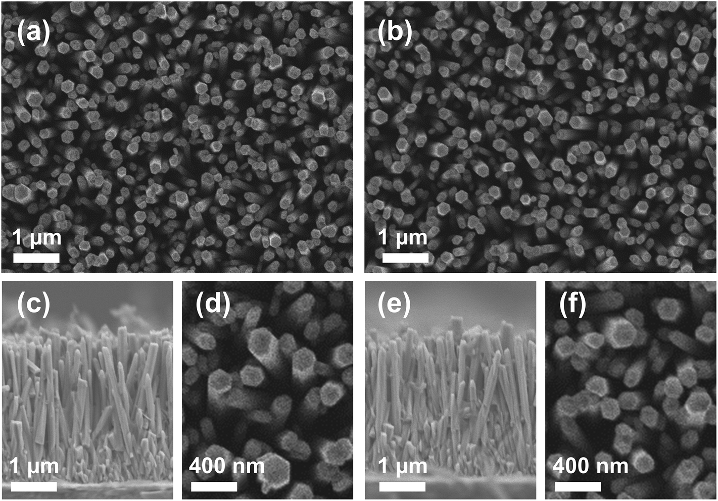 | ||
| Fig. 1 SEM images of the as-grown (a) and N-implanted (b) ZnO NWs. Cross sectional SEM images of the as-grown (c) and N-implanted (e) ZnO NWs. (d) and (f) depict the as-grown and N-implanted ZnO NWs at higher magnification, respectively. | ||
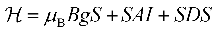
To investigate the origin of acceptors formed in the ZnO NWs upon N implantation we employed the EPR technique, which is known to be among the most powerful and versatile experimental methods for the identification of defects and impurities.51 EPR spectra were analyzed using the following spin-Hamiltonian that includes an electron Zeeman term, a central hyperfine interaction term and a fine structure term:
 | (1) |
Here, S denotes an effective electron spin, I the nuclear spin and B is an external magnetic field. g and A are the electron g-tensor and the hyperfine interaction tensor, respectively, and μB is the Bohr magneton. The fine structure splitting for S > 1/2 is described by the tensor D. The spin-Hamiltonian parameters obtained from fitting the experimental data are summarized in Table 1, together with the parameters of N-related acceptors reported in the literature.51 The substrate does not exhibit any EPR signals and, therefore, all observed EPR signals stem from the ZnO NWs. Fig. 2 shows EPR spectra of the as-grown (b) and N-implanted (a) ZnO NWs measured in the dark B‖c and a microwave frequency of 9.4 GHz (X-band). In both structures the spectra contain a broad feature located at around 335 mT with a g-factor of ∼2.0023. This EPR signal can be attributed to surface dangling bonds.44,52,53 Its observation in the studied NWs reflects a large surface-to-volume ratio in the structures. In the range of magnetic fields typical for shallow donors (∼343 mT) the as-grown ZnO NWs also exhibit at 10 K an EPR signal consisting of one single line (S = 1/2) with a g factor of ∼1.96 – labeled as SD in Fig. 2(a). Such a signal is characteristic of shallow donors in ZnO.51 Since the signal can be detected in the dark, the Fermi level (EF) in the as-grown ZnO NWs must be located above the donor level. This is not surprising as the nominally undoped ZnO usually exhibits n-type conductivity. The shallow donor signal, however, can no longer be detected in the dark after N-implantation, which indicates the formation of compensating acceptors leading to the downshift of EF. Furthermore two new EPR signals are detected in the ZnO:N NWs.
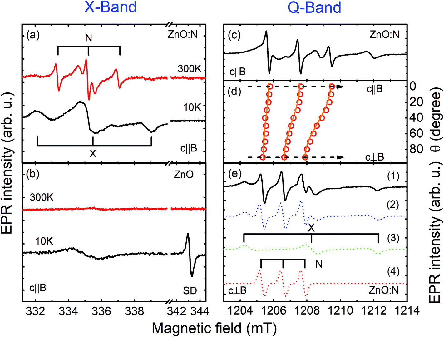 | ||
| Fig. 2 X-Band EPR spectra of the as-grown ZnO NWs (b) and ZnO:N NWs (a) measured in the dark at 10 K and 300 K with B‖c. (c) Q-Band EPR spectrum of the ZnO:N NWs measured at RT with B‖c. (d) The EPR signal from the N-center as a function of the angle θ between B and c. The open circles represent experimental positions of the EPR lines, whereas the solid lines are simulation results using the spin-Hamiltonian in eqn (1) with the parameters given in Table 1. (e) Q-Band EPR spectrum of the ZnO:N NWs (1) measured at RT with B⊥c under white-light illumination. The EPR spectra of the X- and N-center simulated by using eqn (1) are depicted by (3) and (4), respectively. (2) shows the sum of (3) and (4). | ||
| Center | S | I | g ⊥ | g ‖ | |A⊥| | |A‖| | D | E |
|---|---|---|---|---|---|---|---|---|
| NO0 | 1/2 | 1 | 1.9633 | 1.9953 | 9.5 | 81.3 | ||
| N2− | 1/2 | 1 | 1.9935 | 2.0036 | 20.1 | 9.8 | ||
| N-center | 1/2 | 1 | 2.0069 | 2.0054 | 35 | 52 | ||
| X-center | 1 | 2.004 | 2.0035 | 96 | 32 | |||
| SD | 1/2 | 1.955 | 1.957 |
The first one, labeled as X in Fig. 2(a), contains three features: a positive (negative) line at a low (high) magnetic field and a middle line with a derivative line shape. Such a spectrum is typical of a paramagnetic center with an effective electron spin S = 1 in a powder-like system. Consistently, both the splitting between the lines and their line shape are found to be independent of the microwave frequency (9.4 GHz vs. 33 GHz) utilized during the experiments. The best fit to the experimental data can be obtained assuming that the X-center is randomly oriented in the x–y plane (i.e. in the plane orthogonal to the NW growth direction), which likely reflects a random rotation of NWs within this plane, evident in the SEM images shown in Fig. 1. The deduced spin-Hamiltonian parameters are given in Table 1. Due to a lack of a resolved hyperfine structure, no definite chemical identification of this center can be achieved and, therefore, it will not be discussed further here.
The second signal, labeled as N in Fig. 2(a), contains three sharp equidistant lines with the derivative line shape. The splitting between the lines remains the same at different microwave frequencies as seen from Fig. 2(a) and (c), which show EPR spectra measured at the X-band and Q-band, respectively. This rules out the possibility that the lines arise from three different defects with S = 1/2 but slightly different g-values. Instead, the N-center can only be described by assuming a resolved hyperfine interaction with a nuclear spin (I = 1) with almost 100% natural abundance. Nitrogen is the only element that fulfills these criteria, since the 14N isotope has I = 1 and 99.6% natural abundance. In order to gain further insight into the structure of the center, angular dependent EPR studies were performed by rotating from B‖c to B⊥c. The corresponding positions of the EPR lines are shown by the open circles in Fig. 2(d), whereas Fig. 2(e) depicts an experimental spectrum measured in the Q-band with B⊥c. Simulations of the angular-dependent data by using the spin Hamiltonian in eqn (1) yields the set of parameters given in Table 1. The modeling was done considering the random orientations of the NWs in the x–y plane, as well as their tilting by up to 15°. The results of these simulations are shown by the solid lines in Fig. 2(d), as well as by the dashed line (4) in Fig. 2(e), where the simulated EPR spectrum for B⊥c is displayed together with the simulated spectra of other detected EPR signals. Very good agreement between the experimental data and simulation results is observed, justifying the validity of the performed analysis. The N-center is found to exhibit an anisotropic behavior of the g-factor and the hyperfine interaction parameter (see Table 1). The anisotropy of the g-value, with a positive deviation from the free-electron g-value of 2.0023, proves that this defect is an acceptor type. The distribution of the spin density within the defect can be evaluated by analyzing the hyperfine coupling parameter A. A⊥ and A‖ can be expressed in terms of an isotropic part a (Fermi-contact interaction) and an anisotropic part b, by A‖ = a + 2b and A⊥ = a − b. The extracted a and b components can then be compared with the corresponding atomic values of the 2s and 2p orbitals of a free N atom.54,55 This yields  and
and 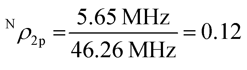 . By employing this qualitative analysis one can deduce the total unpaired electron spin density at the N-center to be Nρtotal = Nρ2s + Nρ2p = 0.146, i.e. about 15%. This in turn indicates that the wavefunction of the unpaired electron bound to the N-center is predominantly of the 2p character (82%), with only 18% in the 2s-orbital, confirming the acceptor origin of the N-center.
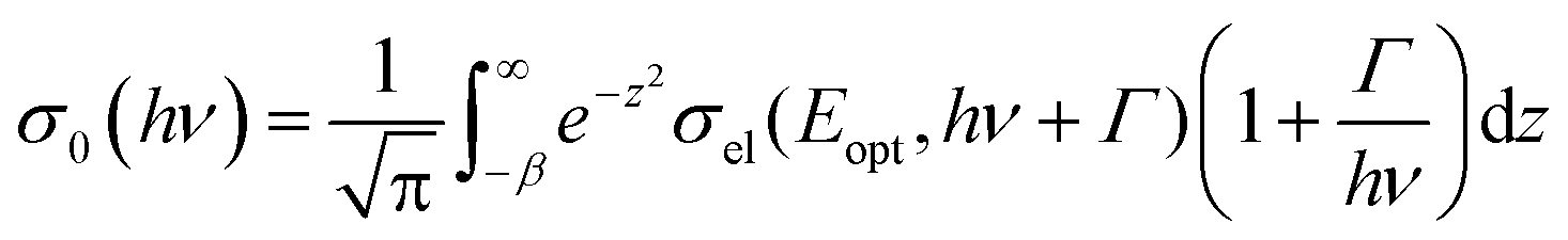
Next, we performed photo-EPR experiments, in order to determine the energy level position of the N-center. The corresponding EPR signal can readily be detected in the dark, but its intensity increases under light illumination when the photon energy exceeds 1.2 eV – see Fig. 3(a). This indicates that the Fermi level is located close to the energy level of the N-center, since some of the centers exist in the paramagnetic (EPR-active) charge state even without illumination while others can be recharged from the diamagnetic (EPR-inactive) charge state to the paramagnetic one due to photon absorption. Moreover, the recharging process exhibits a mono-exponential behavior, as depicted in Fig. 3(b), proving that it is the result of a single photo-ionization process. Since under such conditions no increase in the intensity of the shallow donor EPR signal is detected, the responsible photo-ionization process should occur via the valence band:
| Nn + hν → Nn−1 + h | (2) |
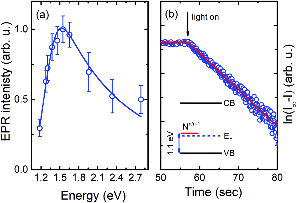 | ||
| Fig. 3 (a) Intensity of the EPR signal from the N-center as a function of the photon energy of light illumination. The solid line represents the best fit to the experimental data by using eqn (3). (b) Time dependent behavior of this signal after switching on the light. The y-axis displays the difference of the measured EPR intensity (I) from the saturation value (I∞) in a log-scale. The inset depicts a schematic energy level diagram. | ||
Here Nn denotes the diamagnetic charge state of the N-center, when it is in the spin paired-off configuration with an even number of bound electrons. Nn−1 denotes, on the other hand, the paramagnetic charge state of the same N-center with an unpaired electron spin when an extra electron is added to the Nn-center. For an acceptor center, n should be equal to or smaller than 0. In other words, the N-center should be either neutral or negatively charged before photo-excitation. Subsequently, the energy level of the N-center can be determined by fitting the experimental data with the expression:56
 | (3) |
Here σel denotes the optical cross section, hν the photon energy and Eopt the optical ionization energy of the center. Taking the electron–phonon interactions into account one obtains:
 | (4) |
 . Γ describes the broadening of the photo transition absorption band at elevated temperatures.
 | (5) |
Fitting of the experimental data shown in Fig. 3(a) yields values of Eopt = (1.3 ± 0.05) eV and Γ = (0.22 ± 0.05) eV. Using these values, Eth can roughly be estimated to be in the range of 1–1.1 eV, which means that the (n/n − 1) level of the N-center is located at approximately 1.1 eV above the top of the valence band (see the inset in Fig. 3(b) for a schematic drawing of the energy level diagram). The N-center is, therefore, a deep acceptor.
Let us now compare the revealed N-center with the N-related acceptors reported in the literature. The deduced spin-Hamiltonian parameters of the N-center are different from the known parameters of NO34,57 and the N2-molecule,58,59 which are commonly observed in N-doped ZnO bulk and thin-films. In addition, it is significantly shallower than the NO and N2 acceptors with their (0/−) energy levels at EVB +1.5 eV (ref. 34, 60 and 61) and EVB +1.9 eV,58,61 respectively. Thus, the N-center uncovered in this work must have a different structure from the two well-known N-related acceptors in ZnO. It has an axial symmetry, i.e. it is likely a complex with a partner located along the crystallographic c-axis. Various N-related complexes have earlier been considered theoretically in bulk ZnO but only a few of them are predicted to be stable and form acceptor states. These include: the (NO–VZn) complex with an (0/−) energy level at EVB +0.13 eV (ref. 37) and the (NZn–2Oi) complex with an (0/−) energy level at EVB +0.55 eV.39 There is also the (NZn–2VZn) complex with an (0/−) energy level at EVB +0.12 eV and an (−/2−) energy level at EVB +0.9 eV.39 However, another study by Petretto et al. places the (0/−) energy level of the (NZn–2VZn) complex at EVB +1.5 eV.61 Among them, only (NO–VZn) has axial symmetry and none of the complexes have an energy level and the charge state matching the N-center revealed in the present work. Our findings, therefore, call for future theoretical studies to understand the structure of N-related acceptors in nanostructured ZnO.
In conclusion, by using EPR spectroscopy we have provided direct experimental evidence that N implantation leads to the formation of N-related acceptors in ZnO NWs. This conclusion is based on (1) the downshift of the Fermi level position in the implanted NWs, evident from the disappearance of the shallow donor-related signal in EPR spectra measured in the dark; and (2) the observation of a new EPR signal of an acceptor origin. This new signal is unambiguously identified to involve an N atom, based on the resolved hyperfine interaction with a nuclear spin I = 1 and almost 100% abundance. The center is further shown to act as an acceptor and has the (n/n − 1) energy level located at about EVB +1.1 eV, i.e. it has a lower ionization energy than the known N-related acceptors in ZnO. Our work, therefore, not only provides the first unambiguous identification of N-related acceptors deliberately incorporated into ZnO nanostructures, but also proves that N can be incorporated in a different configuration in ZnO nanostructures as compared with ZnO bulk and thin-films. The present findings are of importance for understanding the electronic properties of nanostructured ZnO en route towards its future electronic applications.
Conflicts of interest
There are no conflicts of interest to declare.Acknowledgements
Financial support from the Swedish Energy Agency (grant # 43522-1) and the ÅForsk Foundation (grant # 15-433) is gratefully acknowledged.References
- U. Özgür, Y. I. Alivov, C. Liu, A. Teke, M. A. Reshchikov, S. Doğan, V. Avrutin, S.-J. Cho and H. Morkoç, J. Appl. Phys., 2005, 98, 41301 CrossRef.
- S. J. Pearton and F. Ren, Curr. Opin. Chem. Eng., 2014, 3, 51 CrossRef.
- M. Law, L. E. Greene, J. C. Johnson, R. Saykally and P. Yang, Nat. Mater., 2005, 4, 455 CrossRef CAS PubMed.
- J. Guo, J. Zhang, M. Zhu, D. Ju, H. Xu and B. Cao, Sens. Actuators, B, 2014, 199, 333 CrossRef.
- T. P. H. Sidiropoulos, R. Röder, S. Geburt, O. Hess, S. A. Maier, C. Ronning and R. F. Oulton, Nat. Phys., 2014, 10, 870 Search PubMed.
- S. Sergent, M. Takiguchi, T. Tsuchizawa, A. Yokoo, H. Taniyama, E. Kuramochi and M. Notomi, ACS Photonics, 2017, 4, 1040 Search PubMed.
- W. Zhao, X. Xiong, Y. Han, L. Wen, Z. Zou, S. Luo, H. Li, J. Su, T. Zhai and Y. Gao, Adv. Opt. Mater., 2017, 5, 1 Search PubMed.
- X. Ren, X. Zhang, N. Liu, L. Wen, L. Ding, Z. Ma, J. Su, L. Li, J. Han and Y. Gao, Adv. Funct. Mater., 2015, 25, 2182 CrossRef CAS.
- K. M. Lee, C. W. Lai, K. S. Ngai and J. C. Juan, Water Res., 2016, 88, 428 CrossRef CAS PubMed.
- W. Wang, M. O. Tadé and Z. Shao, Prog. Mater. Sci., 2018, 92, 33 CrossRef CAS.
- O. Haibo, H. J. Feng, L. Cuiyan, C. Liyun and F. Jie, Mater. Lett., 2013, 111, 217 CrossRef.
- M. Samadi, M. Zirak, A. Naseri, E. Khorashadizade and A. Z. Moshfegh, Thin Solid Films, 2016, 605, 2 CrossRef CAS.
- S. Sun, X. Chang, X. Li and Z. Li, Ceram. Int., 2013, 39, 5197 CrossRef CAS.
- H. Qin, W. Li, Y. Xia and T. He, ACS Appl. Mater. Interfaces, 2011, 3, 3152 CrossRef CAS PubMed.
- X. Yang, A. Wolcottt, G. Wang, A. Sobo, R. C. Fitzmorris, F. Qian, J. Z. Zhang and Y. Li, Nano Lett., 2009, 9, 2331 CrossRef CAS PubMed.
- T. Minami, H. Sato, H. Nanto and S. Takata, Jpn. J. Appl. Phys., 1985, 24, L781 CrossRef.
- F. Zhang, S. H. Wei and A. Zunger, Phys. Rev. Lett., 2000, 84, 1232 CrossRef PubMed.
- S. B. Zhang, S. H. Wei and A. Zunger, J. Appl. Phys., 1998, 83, 3192 CrossRef CAS.
- D. C. Look, D. C. Reynolds, C. W. Litton, R. L. Jones, D. B. Eason and G. Cantwell, Appl. Phys. Lett., 2002, 81, 1830 CrossRef CAS.
- A. Tsukazaki, A. Ohtomo, T. Onuma, M. Ohtani, T. Makino, M. Sumiya, K. Ohtani, S. F. Chichibu, S. Fuke, Y. Segawa, H. Ohno, H. Koinuma and M. Kawasaki, Nat. Mater., 2004, 4, 42 CrossRef.
- G. D. Yuan, W. J. Zhang, J. S. Jie, X. Fan, J. A. Zapien, Y. H. Leung, L. B. Luo, P. F. Wang, C. S. Lee and S. T. Lee, Nano Lett., 2008, 8, 2591 CrossRef CAS PubMed.
- T. Aoki, Y. Hatanaka and D. C. Look, Appl. Phys. Lett., 2000, 76, 3257 CrossRef CAS.
- B. Xiang, P. Wang, X. Zhang, S. A. Dayeh, D. P. R. Aplin, C. Soci, D. Yu and D. Wang, Nano Lett., 2007, 7, 323 CrossRef CAS PubMed.
- F. X. Xiu, Z. Yang, L. J. Mandalapu, D. T. Zhao, J. L. Liu and W. P. Beyermann, Appl. Phys. Lett., 2005, 87, 1 Search PubMed.
- S. Chu, G. Wang, W. Zhou, Y. Lin, L. Chernyak, J. Zhao, J. Kong, L. Li, J. Ren and J. Liu, Nat. Nanotechnol., 2011, 6, 506 CrossRef CAS PubMed.
- Y. R. Ryu, T. S. Lee and H. W. White, Appl. Phys. Lett., 2003, 83, 87 CrossRef CAS.
- J. Y. Zhang, P. J. Li, H. Sun, X. Shen, T. S. Deng, K. T. Zhu, Q. F. Zhang and J. L. Wu, Appl. Phys. Lett., 2008, 93, 021116 CrossRef.
- M.-P. Lu, M.-Y. Lu and L.-J. Chen, Nano Energy, 2012, 1, 247 CrossRef CAS.
- A. Kobayashi, O. Sankey and J. Dow, Phys. Rev. B: Condens. Matter Mater. Phys., 1983, 28, 946 CrossRef CAS.
- K. Nakahara, S. Akasaka, H. Yuji, K. Tamura, T. Fujii, Y. Nishimoto, D. Takamizu, A. Sasaki, T. Tanabe, H. Takasu, H. Amaike, T. Onuma, S. F. Chichibu, A. Tsukazaki, A. Ohtomo and M. Kawasaki, Appl. Phys. Lett., 2010, 97, 013501 CrossRef.
- C. H. Park, S. B. Zhang and S.-H. Wei, Phys. Rev. B: Condens. Matter Mater. Phys., 2002, 66, 073202 CrossRef.
- J. L. Lyons, A. Janotti and C. G. Van de Walle, Appl. Phys. Lett., 2009, 95, 252105 CrossRef.
- M. C. Tarun, M. Z. Iqbal and M. D. McCluskey, AIP Adv., 2011, 1, 022105 CrossRef.
- J. E. Stehr, D. M. Hofmann and B. K. Meyer, J. Appl. Phys., 2012, 112, 103511 CrossRef.
- J. Li, S.-H. Wei, S.-S. Li and J.-B. Xia, Phys. Rev. B: Condens. Matter Mater. Phys., 2006, 74, 081201 CrossRef.
- T. Yamamoto and H. Katayama-Yoshida, Jpn. J. Appl. Phys., Part 2, 1999, 38, L166 CrossRef CAS.
- L. Liu, J. Xu, D. Wang, M. Jiang, S. Wang, B. Li, Z. Zhang, D. Zhao, C.-X. Shan, B. Yao and D. Z. Shen, Phys. Rev. Lett., 2012, 108, 215501 CrossRef PubMed.
- J. E. Stehr, X. J. Wang, S. Filippov, S. J. Pearton, I. G. Ivanov, W. M. Chen and I. A. Buyanova, J. Appl. Phys., 2013, 113, 103509 CrossRef.
- P. Li, S. Deng, G. Liu and K. Hou, Chem. Phys. Lett., 2012, 543, 92 CrossRef CAS.
- C. Ton-That, L. Zhu, M. N. Lockrey, M. R. Phillips, B. C. C. Cowie, a. Tadich, L. Thomsen, S. Khachadorian, S. Schlichting, N. Jankowski and A. Hoffmann, Phys. Rev. B: Condens. Matter Mater. Phys., 2015, 92, 024103 CrossRef.
- W. R. L. Lambrecht and A. Boonchun, Phys. Rev. B: Condens. Matter Mater. Phys., 2013, 87, 195207 CrossRef.
- S. Haffad, M. Samah and G. Cicero, Phys. Rev. B: Condens. Matter Mater. Phys., 2012, 85, 165207 CrossRef.
- J. Gutjahr, S. Sakong and P. Kratzer, Nanotechnology, 2014, 25, 145204 CrossRef PubMed.
- J. E. Stehr, W. M. Chen, N. K. Reddy, C. W. Tu and I. A. Buyanova, Sci. Rep., 2015, 5, 13406 CrossRef CAS PubMed.
- N. P. Herring, L. S. Panchakarla and M. S. El-Shall, Langmuir, 2014, 30, 2230 CrossRef CAS PubMed.
- Zinc Oxide Bulk, Thin Films and Nanostructures, ed. C. Jagadish and S. Pearton, Elsevier, 2006 Search PubMed.
- C. J. Pan, J. Y. Chen, G. C. Chi, B. W. Chou, B. J. Pong, F. Ren, C. Y. Chang and S. J. Pearton, Vacuum, 2009, 83, 1073 CrossRef CAS.
- F. Friedrich and N. H. Nickel, Appl. Phys. Lett., 2007, 91, 111903 CrossRef.
- M. Wang, F. Ren, J. Zhou, G. Cai, L. Cai, Y. Hu, D. Wang, Y. Liu, L. Guo and S. Shen, Sci. Rep., 2015, 5, 12925 CrossRef CAS PubMed.
- S. Stoll and A. Schweiger, J. Magn. Reson., 2006, 178, 42 CrossRef CAS PubMed.
- J. E. Stehr, B. K. Meyer and D. M. Hofmann, Appl. Magn. Reson., 2010, 39, 137 CrossRef CAS.
- E. Cartier, J. H. Stathis and D. A. Buchanan, Appl. Phys. Lett., 1993, 63, 1510 CrossRef CAS.
- D. J. Miller and D. Haneman, Phys. Rev. B: Solid State, 1971, 3, 2918 CrossRef.
- J. Morton and K. Preston, J. Magn. Reson., 1978, 30, 577 CAS.
- J. a. J. Fitzpatrick, F. R. Manby and C. M. Western, J. Chem. Phys., 2005, 122, 84312 CrossRef PubMed.
- M. Godlewski, Phys. Status Solidi A, 1985, 90, 11 CrossRef CAS.
- W. E. Carlos, E. R. Glaser and D. C. Look, Physica B: Condens. Matter, 2001, 308–310, 976 CrossRef CAS.
- J. M. Philipps, J. E. Stehr, I. A. Buyanova, M. C. Tarun, M. D. McCluskey, B. K. Meyer and D. M. Hofmann, J. Appl. Phys., 2014, 116, 063701 CrossRef.
- N. Y. Garces, L. Wang, N. C. Giles, L. E. Halliburton, G. Cantwell and D. B. Eason, J. Appl. Phys., 2003, 94, 519 CrossRef CAS.
- M. D. McCluskey, Semicond. Semimetals, 2015, 279–313 Search PubMed.
- G. Petretto and F. Bruneval, Phys. Rev. Appl., 2014, 1, 024005 CrossRef.
| This journal is © The Royal Society of Chemistry 2019 |