
 Open Access Article
 This Open Access Article is licensed under a
 Creative Commons Attribution 3.0 Unported Licence
Time-resolved impurity-invisibility in graphene nanoribbons†
Riku
Tuovinen
 *a,
Michael A.
Sentef
a,
Claudia
Gomes da Rocha
b and
Mauro S.
Ferreira
cd
*a,
Michael A.
Sentef
a,
Claudia
Gomes da Rocha
b and
Mauro S.
Ferreira
cd
aMax Planck Institute for the Structure and Dynamics of Matter, 22761 Hamburg, Germany. E-mail: riku.tuovinen@mpsd.mpg.de
bDepartment of Physics and Astronomy, University of Calgary, 2500 University Drive NW, Calgary, Alberta T2N 1N4, Canada
cSchool of Physics, Trinity College Dublin, Dublin 2, Ireland
dCentre for Research on Adaptive Nanostructures and Nanodevices (CRANN) and Advanced Materials and Bioengineering Research (AMBER) Centre, Trinity College Dublin, Dublin 2, Ireland
First published on 10th June 2019
Abstract
We investigate time-resolved charge transport through graphene nanoribbons supplemented with adsorbed impurity atoms. Depending on the location of the impurities with respect to the hexagonal carbon lattice, the transport properties of the system may become invisible to the impurity due to the symmetry properties of the binding mechanism. This motivates a chemical sensing device since dopants affecting the underlying sublattice symmetry of the pristine graphene nanoribbon introduce scattering. Using the time-dependent Landauer–Büttiker formalism, we extend the stationary current–voltage picture to the transient regime, where we observe how the impurity invisibility takes place at sub-picosecond time scales further motivating ultrafast sensor technology. We further characterize time-dependent local charge and current profiles within the nanoribbons, and we identify rearrangements of the current pathways through the nanoribbons due to the impurities. We finally study the behavior of the transients with ac driving which provides another way of identifying the lattice-symmetry breaking caused by the impurities.
1. Introduction
Being under considerable research focus for the past two decades graphene1 and carbon nanotubes2 are known to be extremely sensitive to external perturbations. For this reason, these nanomaterials have been proposed as ideal candidates for sensor technology.3–7 Based on these observations, carbon-based sensor devices have already been developed at the single-molecule resolution.8–11 Carbon-based transducers have been embedded in circuitries involving graphene nanopore platforms12,13 and field effect transistors,14 and these have been successfully applied to, e.g., disentangle biomolecules’ rapid dynamics.15–17 This novel biosensor technology provides real-time information about the underlying physical and chemical mechanisms. These findings motivate ultrafast sensing devices as present transport measurements are able to resolve temporal information at sub-picosecond time scales.18–22These few examples cited above include devices which are interacting with their evolving environment for which a schematic in a quantum transport setup is shown in Fig. 1. The schematics depicts a quantum transport channel made of a graphene nanoribbon (GNR) of armchair configuration with a width characterized by the number of carbon-dimers arranged transversely (N). The ribbon is subjected to a source–drain voltage (VSD) that can vary on time and the whole device serves as a host for detecting the presence of impurities. The main purpose of the voltage bias is to excite the system away from its thermo-chemical equilibrium. We emphasize that the perturbation could be different in practice and still similar intrinsic dynamics would show up, irrespective of the specifics of the perturbation. It would also be feasible to use, e.g., short laser pulses which can perturb the system and then probe the consequent dynamics.23–27 Nonetheless, the theoretical description of these processes is a challenge as these nanoscale devices are operating at high frequencies (THz) so the systems do not necessarily relax to a steady-state configuration instantly. In contrast, there are transient effects depending on, e.g., the system's geometry or topological character,28–33 its predisposition to external perturbations or thermal gradients,34–39 and the physical properties of the transported quanta and their mutual interactions.40–46 There is an increasing demand for theoretical and computational tools capable of addressing, in a general but computationally tractable level, the time-dependent responses of nanomaterials.
 | ||
| Fig. 1 Transport setup of an N = 11 armchair graphene nanoribbon with adsorbed impurity atoms (red spheres) and N indicating the number of carbon-dimers across the ribbon width. Contacts to the metallic leads are from the terminal sites of the nanoribbon. The leads are further connected to a source–drain voltage (VSD). | ||
Motivated by the aforementioned potential that graphene-related materials have for sensor technology, recent theoretical studies5,6 suggested that the bonding symmetry of dopants in graphene plays a major role in defining the strength of the scattering experienced by such systems. In particular, it has been shown that the electronic scattering caused by dopants may be suppressed when they are bound symmetrically to both graphene sublattices, giving rise to impurity invisibility.5,6 In contrast, dopants affecting the two sublattices asymmetrically are more strongly scattered and therefore the most likely candidates to being chemically sensed by graphene. These findings have tremendous potential whereby classifying dopants through their bonding symmetry may lead to a more efficient way of identifying suitable components for graphene-based sensors. However, the results reported in references5,6 were obtained solely on calculations carried out in the stationary regime. Furthermore, no spatial information about the current was provided, which gives little insight on how the impurity invisibility arises from a local viewpoint.
With that in mind, in this manuscript we put the challenge of time-resolved transport calculations to the test and investigate the time-dependent response of a doped GNR in order to establish how the stationary-current regime is reached. In particular, transient-regime responses will be generated with the aim of identifying a signature of impurity invisibility in the time signal. In addition, we spatially map the bond current in the presence of scatterers and pay special attention to how it spreads out for dopants of different bonding symmetries. We argue that recognizing such signatures behind this mechanism is pivotal for efficient design of graphene-based ultrafast chemical sensing devices.
2. Model and method
We consider a system composed of metallic leads α connected to a central molecular structure, where we investigate the (charge) transport of noninteracting electrons. Even though, electron–electron and electron–phonon interaction should, in principle, influence the transport mechanisms,47–50 here we expect our noninteracting picture to be sufficient as recent studies on monolayer graphene devices have revealed ballistic transfer lengths ranging from hundreds of nanometers to even micrometers at low temperatures.51,52 The transport setup (cf.Fig. 1) is partition-free53–55 which means that the whole system is initially contacted in a global thermo-chemical equilibrium at unique chemical potential μ and at inverse temperature β = (kBT)−1 being T the temperature and kB the Boltzmann constant. The central molecular structure is modeled by a tight-binding Hamiltonian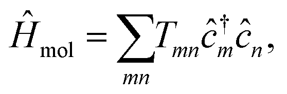 | (1) |
For impurities in the central conducting device we have similarly
 | (2) |
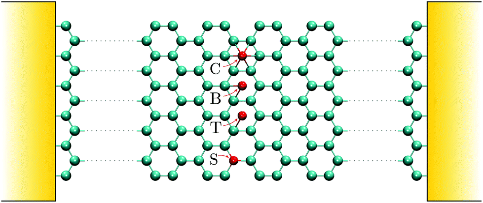 | ||
| Fig. 2 Distinct impurity configurations on a GNR host (cyan atoms). Impurities (red atoms) can be positioned (i) right on the top of a carbon atom (T), (ii) positioned over a carbon–carbon bond characterizing a ‘bridge’ configuration (B), (iii) placed on the center of a hexagonal ring (C), or (iv) substitute a carbon atom (S). | ||
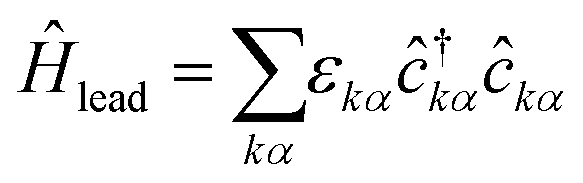
The leads are described as (semi-infinite) reservoirs
 | (3) |
![[thin space (1/6-em)]](https://www.rsc.org/images/entities/char_2009.gif) cosk with tα the hopping energy between the lead's lattice sites. Here we assume that the density of states of the leads is smooth and wide enough allowing us to consider the wide-band approximation (WBA). In WBA, the lead density of states is assumed independent of energy, which in practice means that we choose the energy scales in the leads much higher than other energy scales in the central region. As we concentrate on the effects between the graphene nanoribbon and the impurities this allows us to neglect the precise description of the electronic structure of the leads. This is further justified in typical transport setups where the bandwidth of the leads is sufficiently large (e.g. gold electrodes) compared to the applied bias voltage.39,50,66,67 The leads are connected to the central region by the coupling Hamiltonian
cosk with tα the hopping energy between the lead's lattice sites. Here we assume that the density of states of the leads is smooth and wide enough allowing us to consider the wide-band approximation (WBA). In WBA, the lead density of states is assumed independent of energy, which in practice means that we choose the energy scales in the leads much higher than other energy scales in the central region. As we concentrate on the effects between the graphene nanoribbon and the impurities this allows us to neglect the precise description of the electronic structure of the leads. This is further justified in typical transport setups where the bandwidth of the leads is sufficiently large (e.g. gold electrodes) compared to the applied bias voltage.39,50,66,67 The leads are connected to the central region by the coupling Hamiltonian | (4) |
The total Hamiltonian is then combined as Ĥtot = Ĥmol + Ĥimp + Ĥlead + Ĥcoupl from the contributions in eqn (1)–(4). We consider a switch-on of a bias voltage Vα in lead α at time t = 0 meaning that the lead energy dispersion in eqn (3) becomes εkα → εkα + Vα. Due to this nonequilibrium condition, charge carriers start to flow through the molecular conducting channel, in our case, a GNR. We stress that the coupling matrix elements between the central region and the leads, Tm,kα, are constant at all times as the system is partition-free. Here we consider only voltage biases as mean of perturbation but recently it has also been shown that temperature gradients may be included in this consideration at an equal footing.39,68,69
In the literature, a considerable amount of works uses the method of Landauer and Büttiker (LB)70,71 to determine the transport properties of nanoscale devices as it provides a very simple and intuitive physical picture of the transport mechanism. The current Iαδ in lead δ is calculated from the scattering states originating from lead α ≠ δ. These scattering amplitudes are typically written as transmission probabilities for an electron to traverse from lead α to lead δ. The stationary current in lead δ is obtained from the difference  . Here we also address time-resolved currents, and the nonequilibrium Green's function (NEGF) formalism72 provides a natural framework for this as it is not limited to the stationary state. We describe the time-evolution (transient information) of the system by the NEGF formalism where the Hamiltonian, the Green's function, and correlation effects (self-energies) are coupled by the integro-differential Kadanoff–Baym equations of motion.72 For the model system described above, an analytic solution for the time-dependent one-particle density matrix of the central region and for the time-dependent current between the central region and the leads can be found.73,74 This time-dependent extension to the LB formalism (TD-LB) shares the simple interpretation of the original LB formalism and does not increase the computational cost as it would be the case if one solves numerically the complete Kadanoff–Baym set of equations.75,76 In addition, an arbitrary time-dependence may also be included in the bias voltage, e.g., ac driving.77,78 We emphasize that our method allows for studying the transient and stationary regimes at an equal footing since the stationary LB formula is recovered at the long-time limit t → ∞.
3. Results
We consider GNRs of varying widths with armchair edges in the transport direction (see Fig. 1 and 2). The widths of the GNRs studied here are N = {11, 12} with N indicating the number of carbon-dimers across the ribbon width representing, respectively, the metallic and semiconducting families of armchair GNRs: N = 3p − 1 and N = 3p with p an integer number.79,80 In addition to the pristine GNR, we consider impurities being adsorbed or substitutionally placed over the GNR host as shown in Fig. 2. The impurities can connect to the pristine GNR in four different configurations: ‘Center’ (C), ‘Bridge’ (B), ‘Top’ (T), and ‘Substitutional’ (S).5 For the impurities, we set εimp = 0.66γ and γimp = −2.2γ in eqn (2).62 The left-most atoms of the graphene nanoribbon are connected to the left lead and the right-most atoms to the right lead, as depicted in Fig. 2. The length of the GNR in the transport direction is 10 hexagons (≈4 nm) which is large compared to the impurity section. This choice is justified also because the overall transient features have been shown to scale with the length of the GNRs.73 For the sake of simplicity, we study transient responses when the GNR is subjected to adsorption of 4 impurities; these correspond to the four centermost hexagons in the GNR as shown in Fig. 2. More complex chemical perturbations such as increase in the number of impurities, asymmetric bonds, random distribution of impurities etc.81–83 could also be addressed with the same theoretical toolbox. However, our understanding can benefit from such simplified picture that enables us to address this problem with mathematical transparency. In this way, we can identify with clarity on typical transport patterns and universal responses in a class of impurities that attach to the graphene lattice following these particular bonding symmetries.Current–voltage characteristics
We start by setting a source–drain voltage, VSD ≡ VL − VR, over a GNR section sandwiched by left (L) and right (R) leads and evaluate the stationary current with I = (IL + IR)/2 where IL and IR are the currents through the left and right interface, respectively. This gives I–V curves as seen in Fig. 3. From the current–voltage characteristics, we see that placing the impurities on the Center configuration, in general, corresponds to impurity-invisibility5 as the curves are essentially on top of the pristine ones. We have tested with different on-site and hopping energy parameters for the impurity that this symmetric configuration gives rise to vanishingly small scattering regardless of the specifics of the impurity. The only deviation between the pristine and Center configurations is seen in a very small bias voltage window in the N = 12 ribbon (see inset in Fig. 3(b)). This effect could be related to Anderson localization, due to disorder induced by the impurities, leading to a metal–insulator transition.84,85 In general, from Fig. 3, we confirm that the pristine N = 11 ribbon is metallic (nonzero slope at zero bias), and doping with the Bridge configuration makes the ribbon more metallic-like while doping with the Top configuration makes the ribbon more semiconducting-like. Also, the pristine N = 12 ribbon is semiconducting and the other configurations show that the absolute values of the stationary currents are smaller, i.e., the impurities introduce scattering to some extent. In general, we also observe by evaluating dI/dV in units of the conductance quantum 2e2/h ≈ 77 μS that the low-voltage regime can be related to this scale as a single-band transport channel close to the Fermi energy connected to idealized contacts. | ||
| Fig. 3 Current–voltage characteristics of a (a) N = 11 and (b) N = 12 GNR in pristine and adsorbed/doped forms. Adatoms are placed on the center, bridge, top, and substitutional configurations as specified in Fig. 2. The insets show a zoom-in at the low-voltage regime. | ||
Current transients
Now we investigate, how the stationary state in Fig. 3 is reached from the transient regime. As we observed some albeit small different behavior at small and large voltages, we performed transient calculations also in these two regimes by fixing the bias voltage to VSD/2 = 0.05γ and VSD/2 = 1.2γ, respectively. We evaluate the time-dependent current by the same definition as the stationary ones, i.e., as instantaneous left-right average I(t) = (IL(t) + IR(t))/2. We note that this information is directly obtained from the single-time Green's function whereas double-time Green's functions would be needed for current correlations or noise.86The time-dependent current signals are shown in Fig. 4 where we depict the initial transient behaviour (up to 30 fs) and also the long-time limit (up to 500 fs) at which we observed saturation of the currents. At small voltages, there is considerable difference between the pristine and Center configurations during the transient. As seen from Fig. 3, they saturate to the same value for the N = 11 ribbon and to a different value for the N = 12 ribbon. Larger voltages (cf.Fig. 5) bring more transient features but we see that in both N = 11 and N = 12 ribbons the pristine and Center configurations saturate essentially to the same value, although during the transient they can be very different. At higher voltages, Top and Bridge configurations take very long times to saturate (hundreds of femtoseconds); these impurity states introduce a considerable amount of back-and-forth scattering, which is not coupled to the leads, and these states have a long lifetime resulting in very slow damping.
 | ||
| Fig. 4 Time-dependent currents driven by a small bias voltage VSD/2 = 0.05γ through the (a) N = 11 and (b) N = 12 ribbons. The long-time limit of the currents is shown as a cutout of the plot panel on the right-hand side. | ||
 | ||
| Fig. 5 Same as Fig. 4 but with a large bias voltage VSD/2 = 1.2γ. | ||
Another important point to note from these results, as we consider particle-hole symmetric cases for the central region, and we apply a symmetric bias voltage, VL = −VR, our left and right currents are equal. Therefore we observe no charge cumulation or depletion within the central region, and there is no need to take into account, e.g., charging energy or Coulomb blockade.43
Local charge densities and bond currents
As we have seen above, even if the time-dependent currents through the nanoribbons saturate to expected values from stationary calculations, during the transient the currents oscillate significantly. In addition to the interface currents between the nanoribbons and the leads, we now investigate the local charge fluctuations and bond current patterns within the entire samples. In order to access this information, we need to evaluate the full one-particle density matrix, where the diagonal elements correspond to the local site densities and the off-diagonal elements correspond to the bond currents between the sites.73 We concentrate on the initial transient to understand how the role of impurities affects the formation of the stationary state, and we focus our discussion on two representative impurity configurations, Center and Bridge. Complete results including animations depicting charge propagation in time are shown in the ESI.†87From the time-dependent currents in Fig. 4 and 5 and from the snapshots in Fig. 6 and 7, we see that, even though the stationary current through the Center configuration is mostly unaffected by the impurity sites, in the transient regime the impurities provide a “shock absorber” for the initial density wavefront. In the Center configuration, the density wavefronts undergo a symmetry-driven destructive interference, and the opposing bond currents cancel each other. This transparency is lifted once the lattice symmetry of the system is broken in other impurity configurations. This effect is observed by the decreased initial current peak at small voltages in Fig. 4, and as modified transient oscillations at high voltages in Fig. 5. The snapshots in Fig. 6 and 7 show the density variation (with respect to the ground state) and bond-current profiles before the first collision of the density wavefronts at the middle of the ribbons (t = 2 fs), and later when the wavepackets are reflecting from the lead interfaces back to the middle of the ribbons (t = 22 fs). We see how the Bridge configuration introduces a peculiarly locked current pattern around the impurity atoms. This effect results in a remarkably partitioned charge distribution compared to the Center configuration. This partitioned profile results mostly from the impurity induced electronic scattering that takes place at the interfaces between the pristine and doped parts of the graphene ribbon. However, there is no topological zero mode associated with the impurity states, although related effects might also be possible to engineer.88,89
 | ||
| Fig. 6 Snapshots of the local charge densities (colorful circles) and bond currents (black arrows) along the nanoribbons during the initial transient due to a small bias voltage, VSD/2 = 0.05γ. These charge density plots show the difference between the charge density at time t and the ground-state density (in units of e) computed atom-by-atom (color map). The strength of the bond current is indicated by the width of the black arrows. | ||
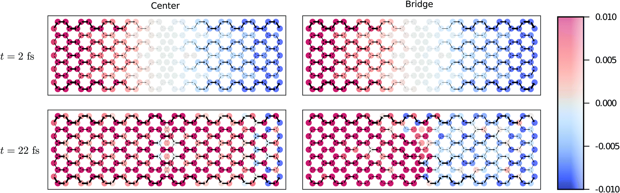 | ||
| Fig. 7 Same as Fig. 6 but with a large bias voltage, VSD/2 = 1.2γ. (Note the different scale on the color bar.). | ||
The full dynamics is better visualized by animations in the ESI.†87 From the animations we may also see how the overall current pathways through the ribbon are modified by the impurities in real time. We note in passing that we observe, similar to reference,5 that the top-bonded impurities are strong scatterers compared to other impurity configurations, and the local bond-current profiles significantly rearrange and focus due to the impurities.32,87 We can also identify specific symmetries in the simulated charge and current profiles. Clearly, the Center configuration respects two mirror symmetries, and we observe both charge density and bond currents obeying these at all times.87
Transient charge pumping
We have seen above how breaking the lattice symmetry of the unbiased graphene sample by introducing impurities leads to different signals both in the transient and stationary regimes. The symmetry of the transport setup can also be broken by the driving mechanism, and thus, we consider charge pumping through the graphene samples78,90–95 in the transient regime. In contrast to the previous sections, we now introduce a harmonic driving VL = −VR = V(t) with the voltage profile| V(t) = V0 + Acos(Ωt) | (5) |
In Fig. 8, we show for the N = 11 ribbons, the current responses to the two different drives described above, and also the corresponding Fourier spectra. For better frequency resolution, the Fourier transform is calculated from an extended temporal window up to 500 fs, and Blackman-window filtering is used. We see from Fig. 8(a) and (c) that even if the time-dependent signals are essentially on top of each other for all the impurity configurations (within this temporal window), the frequency content is still different. The pristine ribbon expectedly excludes the even harmonics, showing pronounced peaks at ω = (2n + 1)Ω with n being an integer number only, due to the odd-inversion-symmetric drive. However, introducing any impurities (even in the Center configuration) breaks the corresponding symmetry of the time-independent Hamiltonian, and peaks at even multiples (ω = 2nΩ) of the driving frequency also appear. In Fig. 8(b) the odd-inversion symmetry of the drive is already broken, so all the ribbons including the Pristine show pronounced peaks in the Fourier spectra also at the even multiples of the driving frequency. In addition, we see that in both cases peaks up to very high harmonic order are visible, indicating operation far beyond the linear-response regime.
 | ||
| Fig. 8 Time-dependent currents through the N = 11 ribbons driven by ac bias voltage. Current responses to (a) an odd-inversion-symmetric drive, and (b) a broken-inversion-symmetric drive. (c) The corresponding Fourier transforms for odd and even symmetries of the drive. | ||
4. Conclusions
We presented a time-resolved characterization of impurity invisibility in graphene nanoribbons. Our transport setup of graphene nanoribbons supplemented with impurities was described by a single-π-orbital tight-binding framework where the impurity atoms were modeled by modified tight-binding parameters compared to the pristine graphene nanoribbons. We accessed the transport properties both at stationary and transient regimes by the TD-LB formalism, allowing for a fast and accurate simulation based on the NEGF method.72,96Our stationary results showed that the center-bonded impurities in graphene are invisible to conduction electrons being unable to scatter them.5,6,85 We then compared the time-dependent build-up of a steady-state current after a sudden quench of the bias voltage for different impurity configurations, and we discovered that the dynamics for different configurations look significantly different. Further, our spatio-temporal-resolved results showed that the impurities induce rearrangement and focusing of the current pathways along the graphene nanoribbons. In addition to the stationary picture, we further argue that graphene nanoribbons could serve as excellent probes or chemical sensors via ultrafast transport measurements.18–22
Driving the graphene samples with strong ac bias voltage was shown to lead to highly nonlinear behavior. The resulting high-harmonic responses were shown to contain selective even–odd signals implying a generation of distinct on–off signals from an analog source which could be further realized as ac–dc conversion or rectification. This mechanism could be considered with photon-assisted tunneling of electrons only permitted to occur from sidebands lying at odd or even multiples of the basic driving frequency. The resulting transient times can be of the same order as the plasma oscillation period of charge profiles sloshing back and forth along the graphene nanoribbons. These findings further highlight the great potential sensing devices probing ultrafast modifications in the sample, the general design of efficient circuitries, and engineering of plasmonic and optical nanoscale devices.97–101
Conflicts of interest
There are no conflicts to declare.Acknowledgements
R. T. and M. A. S. acknowledge funding by the DFG (Grant No. SE 2558/2-1) through the Emmy Noether program. C. G. R. acknowledges WestGrid (http://www.westgrid.ca) and Compute Canada Calcul Canada (http://www.computecanada.ca) for computational resources.References
- K. S. Novoselov, A. K. Geim, S. V. Morozov, D. Jiang, M. I. Katsnelson, I. V. Grigorieva, S. V. Dubonos and A. A. Firsov, Nature, 2005, 438, 197 CrossRef CAS PubMed.
- S. Iijima, Nature, 1991, 354, 56 CrossRef CAS.
- G. Gruner, Anal. Bioanal. Chem., 2006, 384, 322 CrossRef CAS PubMed.
- D. Rodrigo, O. Limaj, D. Janner, D. Etezadi, F. J. García de Abajo, V. Pruneri and H. Altug, Science, 2015, 349, 165 CrossRef CAS PubMed.
- J. Duffy, J. Lawlor, C. Lewenkopf and M. S. Ferreira, Phys. Rev. B, 2016, 94, 045417 CrossRef.
- D. A. Ruiz-Tijerina and L. G. G. V. Dias da Silva, Phys. Rev. B, 2016, 94, 085425 CrossRef.
- B. R. Goldsmith, L. Locascio, Y. Gao, M. Lerner, A. Walker, J. Lerner, J. Kyaw, A. Shue, S. Afsahi, D. Pan, J. Nokes and F. Barron, Sci. Rep., 2019, 9, 434 CrossRef PubMed.
- K. Besteman, J.-O. Lee, F. G. M. Wiertz, H. A. Heering and C. Dekker, Nano Lett., 2003, 3, 727 CrossRef CAS.
- H.-M. So, K. Won, Y. H. Kim, B.-K. Kim, B. H. Ryu, P. S. Na, H. Kim and J.-O. Lee, J. Am. Chem. Soc., 2005, 127, 11906 CrossRef CAS PubMed.
- Y. Choi, T. J. Olsen, P. C. Sims, I. S. Moody, B. L. Corso, M. N. Dang, G. A. Weiss and P. G. Collins, Nano Lett., 2013, 13, 625 CrossRef CAS PubMed.
- B. N. Shivananju, W. Yu, Y. Liu, Y. Zhang, B. Lin, S. Li and Q. Bao, Adv. Funct. Mater., 2016, 27, 1603918 CrossRef.
- C. A. Merchant, K. Healy, M. Wanunu, V. Ray, N. Peterman, J. Bartel, M. D. Fischbein, K. Venta, Z. Luo, A. T. C. Johnson and M. Drndic, Nano Lett., 2010, 10, 2915 CrossRef CAS PubMed.
- S. M. Avdoshenko, D. Nozaki, C. G. Rocha, J. W. González, M. H. Lee, R. Gutierrez and G. Cuniberti, Nano Lett., 2013, 13, 1969–1976 CrossRef CAS PubMed.
- Y. Choi, I. S. Moody, P. C. Sims, S. R. Hunt, B. L. Corso, D. E. Seitz, L. C. Blaszczak, P. G. Collins and G. A. Weiss, J. Am. Chem. Soc., 2012, 134, 2032 CrossRef CAS PubMed.
- G. F. Schneider, S. W. Kowalczyk, V. E. Calado, G. Pandraud, H. W. Zandbergen, L. M. K. Vandersypen and C. Dekker, Nano Lett., 2010, 10, 3163–3167 CrossRef CAS PubMed.
- S. Garaj, W. Hubbard, A. Reina, J. Kong, D. Branton and J. A. Golovchenko, Nature, 2010, 467, 190 CrossRef CAS PubMed.
- F. Traversi, C. Raillon, S. M. Benameur, K. Liu, S. Khlybov, M. Tosun, D. Krasnozhon, A. Kis and A. Radenovic, Nat. Nanotechnol., 2013, 8, 939 CrossRef CAS PubMed.
- L. Prechtel, L. Song, D. Schuh, P. Ajayan, W. Wegscheider and A. W. Holleitner, Nat. Commun., 2012, 3, 646 CrossRef PubMed.
- N. Hunter, A. S. Mayorov, C. D. Wood, C. Russell, L. Li, E. H. Linfield, A. G. Davies and J. E. Cunningham, Nano Lett., 2015, 15, 1591 CrossRef CAS PubMed.
- M. Rashidi, J. A. J. Burgess, M. Taucer, R. Achal, J. L. Pitters, S. Loth and R. A. Wolkow, Nat. Commun., 2016, 7, 13258 CrossRef CAS PubMed.
- C. Karnetzky, P. Zimmermann, C. Trummer, C. Duque Sierra, M. Wörle, R. Kienberger and A. Holleitner, Nat. Commun., 2018, 9, 2471 CrossRef PubMed.
- J. W. McIver, B. Schulte, F. U. Stein, T. Matsuyama, G. Jotzu, G. Meier and A. Cavalleri, 2018, arXiv:1811.03522.
- F. Schmitt, P. S. Kirchmann, U. Bovensiepen, R. G. Moore, L. Rettig, M. Krenz, J.-H. Chu, N. Ru, L. Perfetti, D. H. Lu, M. Wolf, I. R. Fisher and Z.-X. Shen, Science, 2008, 321, 1649 CrossRef CAS PubMed.
- R. Matsunaga, Y. I. Hamada, K. Makise, Y. Uzawa, H. Terai, Z. Wang and R. Shimano, Phys. Rev. Lett., 2013, 111, 057002 CrossRef PubMed.
- A. F. Kemper, M. A. Sentef, B. Moritz, J. K. Freericks and T. P. Devereaux, Phys. Rev. B: Condens. Matter Mater. Phys., 2015, 92, 224517 CrossRef.
- M. A. Sentef, A. Tokuno, A. Georges and C. Kollath, Phys. Rev. Lett., 2017, 118, 087002 CrossRef CAS PubMed.
- D. Werdehausen, T. Takayama, M. Höppner, G. Albrecht, A. W. Rost, Y. Lu, D. Manske, H. Takagi and S. Kaiser, Sci. Adv., 2018, 4, eaap8652 CrossRef PubMed.
- E. Khosravi, G. Stefanucci, S. Kurth and E. Gross, Phys. Chem. Chem. Phys., 2009, 11, 4535 RSC.
- E. Perfetto, G. Stefanucci and M. Cini, Phys. Rev. B: Condens. Matter Mater. Phys., 2010, 82, 035446 CrossRef.
- D. Vieira, K. Capelle and C. A. Ullrich, Phys. Chem. Chem. Phys., 2009, 11, 4647 RSC.
- B. Wang, J. Li, F. Xu, Y. Wei, J. Wang and H. Guo, Nanoscale, 2015, 7, 10030 RSC.
- C. G. Rocha, R. Tuovinen, R. van Leeuwen and P. Koskinen, Nanoscale, 2015, 7, 8627 RSC.
- R. Tuovinen, E. Perfetto, R. van Leeuwen, G. Stefanucci and M. A. Sentef, 2019, arXiv:1902.05821.
- S. Kurth, G. Stefanucci, E. Khosravi, C. Verdozzi and E. K. U. Gross, Phys. Rev. Lett., 2010, 104, 236801 CrossRef CAS PubMed.
- F. Foieri and L. Arrachea, Phys. Rev. B: Condens. Matter Mater. Phys., 2010, 82, 125434 CrossRef.
- L. Arrachea, E. R. Mucciolo, C. Chamon and R. B. Capaz, Phys. Rev. B: Condens. Matter Mater. Phys., 2012, 86, 125424 CrossRef.
- H. Ness and L. K. Dash, Phys. Rev. B: Condens. Matter Mater. Phys., 2011, 84, 235428 CrossRef.
- R. Tuovinen, N. Säkkinen, D. Karlsson, G. Stefanucci and R. van Leeuwen, Phys. Rev. B, 2016, 93, 214301 CrossRef.
- F. Covito, F. G. Eich, R. Tuovinen, M. A. Sentef and A. Rubio, J. Chem. Theory Comput., 2018, 14, 2495 CrossRef CAS PubMed.
- H. O. Wijewardane and C. A. Ullrich, Phys. Rev. Lett., 2005, 95, 086401 CrossRef CAS PubMed.
- P. Myöhänen, A. Stan, G. Stefanucci and R. van Leeuwen, EPL, 2008, 84, 67001 CrossRef.
- A.-M. Uimonen, E. Khosravi, A. Stan, G. Stefanucci, S. Kurth, R. van Leeuwen and E. K. U. Gross, Phys. Rev. B: Condens. Matter Mater. Phys., 2011, 84, 115103 CrossRef.
- P. Myöhänen, R. Tuovinen, T. Korhonen, G. Stefanucci and R. van Leeuwen, Phys. Rev. B: Condens. Matter Mater. Phys., 2012, 85, 075105 CrossRef.
- S. Latini, E. Perfetto, A.-M. Uimonen, R. van Leeuwen and G. Stefanucci, Phys. Rev. B: Condens. Matter Mater. Phys., 2014, 89, 075306 CrossRef.
- C. Verdozzi, G. Stefanucci and C.-O. Almbladh, Phys. Rev. Lett., 2006, 97, 046603 CrossRef PubMed.
- R. Tuovinen, D. Golež, M. Schüler, P. Werner, M. Eckstein and M. A. Sentef, Phys. Status Solidi B, 2018 DOI:10.1002/pssb.201800469.
- M. Galperin, M. A. Ratner and A. Nitzan, J. Phys.: Condens. Matter, 2007, 19, 103201 CrossRef.
- D. W. Swenson, G. Cohen and E. Rabani, Mol. Phys., 2012, 110, 743–750 CrossRef CAS.
- R. Härtle, G. Cohen, D. R. Reichman and A. J. Millis, Phys. Rev. B: Condens. Matter Mater. Phys., 2013, 88, 235426 CrossRef.
- M. Ridley, E. Gull and G. Cohen, 2019, arXiv:1903.07361.
- F. Miao, S. Wijeratne, Y. Zhang, U. C. Coskun, W. Bao and C. N. Lau, Science, 2007, 317, 1530 CrossRef CAS PubMed.
- Y.-M. Lin, K. A. Jenkins, A. Valdes-Garcia, J. P. Small, D. B. Farmer and P. Avouris, Nano Lett., 2009, 9, 422–426 CrossRef CAS PubMed.
- M. Cini, Phys. Rev. B: Condens. Matter Mater. Phys., 1980, 22, 5887 CrossRef.
- G. Stefanucci and C.-O. Almbladh, Phys. Rev. B: Condens. Matter Mater. Phys., 2004, 69, 195318 CrossRef.
- M. Ridley and R. Tuovinen, J. Low Temp. Phys., 2018, 191, 380 CrossRef CAS.
- S. Reich, J. Maultzsch, C. Thomsen and P. Ordejón, Phys. Rev. B: Condens. Matter Mater. Phys., 2002, 66, 035412 CrossRef.
- A. H. Castro Neto, F. Guinea, N. M. R. Peres, K. S. Novoselov and A. K. Geim, Rev. Mod. Phys., 2009, 81, 109 CrossRef CAS.
- Y. Hancock, A. Uppstu, K. Saloriutta, A. Harju and M. J. Puska, Phys. Rev. B: Condens. Matter Mater. Phys., 2010, 81, 245402 CrossRef.
- R. Kundu, Mod. Phys. Lett. B, 2011, 25, 163–173 CrossRef CAS.
- V.-T. Tran, J. Saint-Martin, P. Dollfus and S. Volz, AIP Adv., 2017, 7, 075212 CrossRef.
- J.-P. Joost, N. Schlünzen and M. Bonitz, Phys. Status Solidi B, 2018 DOI:10.1002/pssb.201800498.
- J. P. Robinson, H. Schomerus, L. Oroszlány and V. I. Fal'ko, Phys. Rev. Lett., 2008, 101, 196803 CrossRef PubMed.
- T. O. Wehling, S. Yuan, A. I. Lichtenstein, A. K. Geim and M. I. Katsnelson, Phys. Rev. Lett., 2010, 105, 056802 CrossRef CAS PubMed.
- S. Ihnatsenka and G. Kirczenow, Phys. Rev. B: Condens. Matter Mater. Phys., 2011, 83, 245431 CrossRef.
- V. O. Shubnyi, Y. V. Skrypnyk, S. G. Sharapov and V. M. Loktev, 2019, arXiv:1903.10363.
- Y. Zhu, J. Maciejko, T. Ji, H. Guo and J. Wang, Phys. Rev. B: Condens. Matter Mater. Phys., 2005, 71, 075317 CrossRef.
- C. J. O. Verzijl, J. S. Seldenthuis and J. M. Thijssen, J. Chem. Phys., 2013, 138, 094102 CrossRef CAS PubMed.
- F. G. Eich, A. Principi, M. Di Ventra and G. Vignale, Phys. Rev. B: Condens. Matter Mater. Phys., 2014, 90, 115116 CrossRef.
- F. G. Eich, M. Di Ventra and G. Vignale, Phys. Rev. B, 2016, 93, 134309 CrossRef.
- R. Landauer, Philos. Mag., 1970, 21, 863 CrossRef CAS.
- M. Büttiker, Phys. Rev. Lett., 1986, 57, 1761 CrossRef PubMed.
- G. Stefanucci and R. van Leeuwen, Nonequilibrium Many-Body Theory of Quantum systems: A Modern Introduction, Cambridge University Press, 2013 Search PubMed.
- R. Tuovinen, E. Perfetto, G. Stefanucci and R. van Leeuwen, Phys. Rev. B: Condens. Matter Mater. Phys., 2014, 89, 085131 CrossRef.
- R. Tuovinen, R. van Leeuwen, E. Perfetto and G. Stefanucci, J. Phys.: Conf. Ser., 2016, 696, 012016 CrossRef.
- N. E. Dahlen and R. van Leeuwen, Phys. Rev. Lett., 2007, 98, 153004 CrossRef PubMed.
- A. Stan, N. E. Dahlen and R. van Leeuwen, J. Chem. Phys., 2009, 130, 224101 CrossRef PubMed.
- M. Ridley, A. MacKinnon and L. Kantorovich, Phys. Rev. B: Condens. Matter Mater. Phys., 2015, 91, 125433 CrossRef.
- M. Ridley and R. Tuovinen, Phys. Rev. B, 2017, 96, 195429 CrossRef.
- D. Prezzi, D. Varsano, A. Ruini, A. Marini and E. Molinari, Phys. Rev. B: Condens. Matter Mater. Phys., 2008, 77, 041404 CrossRef.
- A. Kimouche, M. M. Ervasti, R. Drost, S. Halonen, A. Harju, P. M. Joensuu, J. Sainio and P. Liljeroth, Nat. Commun., 2015, 6, 10177 CrossRef CAS PubMed.
- J. A. Fürst, J. G. Pedersen, C. Flindt, N. A. Mortensen, M. Brandbyge, T. G. Pedersen and A.-P. Jauho, New J. Phys., 2009, 11, 095020 CrossRef.
- M. M. Ervasti, Z. Fan, A. Uppstu, A. V. Krasheninnikov and A. Harju, Phys. Rev. B: Condens. Matter Mater. Phys., 2015, 92, 235412 CrossRef.
- S. J. Brun, V. M. Pereira and T. G. Pedersen, Phys. Rev. B, 2016, 93, 245420 CrossRef.
- J. H. García, B. Uchoa, L. Covaci and T. G. Rappoport, Phys. Rev. B: Condens. Matter Mater. Phys., 2014, 90, 085425 CrossRef.
- S. Irmer, D. Kochan, J. Lee and J. Fabian, Phys. Rev. B, 2018, 97, 075417 CrossRef CAS.
- M. Ridley, A. MacKinnon and L. Kantorovich, Phys. Rev. B, 2017, 95, 165440 CrossRef.
- See ESI† for the animations corresponding to the snapshots in Fig. 6 and 7.
- D. J. Rizzo, G. Veber, T. Cao, C. Bronner, T. Chen, F. Zhao, H. Rodriguez, S. G. Louie, M. F. Crommie and F. R. Fischer, Nature, 2018, 560, 204–208 CrossRef CAS PubMed.
- B. A. Barker, A. J. Bradley, M. M. Ugeda, S. Coh, A. Zettl, M. F. Crommie, S. G. Louie and M. L. Cohen, Phys. Rev. B, 2019, 99, 075431 CrossRef CAS.
- C. G. Rocha, L. E. F. Foa Torres and G. Cuniberti, Phys. Rev. B: Condens. Matter Mater. Phys., 2010, 81, 115435 CrossRef.
- L. E. F. Foa Torres, H. L. Calvo, C. G. Rocha and G. Cuniberti, Appl. Phys. Lett., 2011, 99, 092102 CrossRef.
- M. R. Connolly, K. L. Chiu, S. P. Giblin, M. Kataoka, J. D. Fletcher, C. Chua, J. P. Griffiths, G. A. C. Jones, V. I. Fal'ko, C. G. Smith and T. J. B. M. Janssen, Nat. Nanotechnol., 2013, 8, 417 CrossRef CAS PubMed.
- G. Jnawali, Y. Rao, H. Yan and T. F. Heinz, Nano Lett., 2013, 13, 524 CrossRef CAS PubMed.
- J. Zhang, J. Schmalian, T. Li and J. Wang, J. Phys.: Condens. Matter, 2013, 25, 314201 CrossRef PubMed.
- M. J. Wang, J. Wang and J. F. Liu, EPL, 2018, 121, 47002 CrossRef.
- R. Tuovinen, Ph.D. thesis, University of Jyväskylä, 2016 Search PubMed.
- R. Baer, T. Seideman, S. Ilani and D. Neuhauser, J. Chem. Phys., 2004, 120, 3387 CrossRef CAS PubMed.
- V. Ryzhii, T. Otsuji, M. Ryzhii and M. S. Shur, J. Phys. D: Appl. Phys., 2012, 45, 302001 CrossRef.
- W. Gao, J. Shu, K. Reichel, D. V. Nickel, X. He, G. Shi, R. Vajtai, P. M. Ajayan, J. Kono, D. M. Mittleman and Q. Xu, Nano Lett., 2014, 14, 1242–1248 CrossRef CAS PubMed.
- D. C. Marinica, M. Zapata, P. Nordlander, A. K. Kazansky, P. M. Echenique, J. Aizpurua and A. G. Borisov, Sci. Adv., 2015, 1, e1501095 CrossRef PubMed.
- L. Lin, M. Zapata, M. Xiong, Z. Liu, S. Wang, H. Xu, A. G. Borisov, H. Gu, P. Nordlander, J. Aizpurua and J. Ye, Nano Lett., 2015, 15, 6419 CrossRef CAS PubMed.
Footnote |
| † Electronic supplementary information (ESI) available: Animations corresponding to the snapshots in Fig. 6 and 7. See DOI: 10.1039/C9NR02738F |
| This journal is © The Royal Society of Chemistry 2019 |