
 Open Access Article
 This Open Access Article is licensed under a
 Creative Commons Attribution 3.0 Unported Licence
Single-walled carbon nanotube layers for millimeter-wave beam steering†
Serguei
Smirnov
 a,
Dmitri V.
Lioubtchenko
*ab and
Joachim
Oberhammer
a
a,
Dmitri V.
Lioubtchenko
*ab and
Joachim
Oberhammer
a
aDepartment of Micro and Nanosystems, KTH Royal Institute of Technology, Malvinas väg 10, SE-100 44 Stockholm, Sweden. E-mail: dml@kth.se
bCenter for Terahertz Research and Applications, Institute for High Pressure Physics, PAS, 29/37 Sokołowska Str, 01-142 Warsaw, Poland
First published on 12th July 2019
Abstract
The ability to efficiently transmit and manipulate high-frequency signals poses major challenges resulting in a lack of active and reconfigurable millimeter-wave and terahertz devices that are needed to enable beyond-5G broadband communication systems. Here, thin single-walled carbon nanotube (SWCNT) layers are introduced as a tunable impedance surface for millimeter-waves. Carbon nanotube layers are integrated with dielectric rod waveguides. Their surface impedance, tuned by light, is shown to modify the wave propagation inside the waveguide. A direct application of the effect is a phase shifter, demonstrated experimentally and by numerical simulations. Additionally, an antenna array of two dielectric waveguides, one covered in SWCNTs, is designed and fabricated. The proof-of-concept illustrates optically-controlled beam steering enabled by carbon nanotubes, and directions for further device optimizations are provided. These findings demonstrate thin SWCNT layers as an optically-reconfigurable element, suitable for broadband millimeter-wave communications.
Introduction
Mobile broadband networks experience a continuous increase in the number of mobile users, with an urge for faster internet access, advanced multimedia capabilities, and increasingly wireless devices.1,2 However, this growth poses several challenges to cellular operators, such as ensuring higher data rates, larger network capacity, higher mobility and coverage, higher spectral efficiency, and better energy efficiency.3,4 The envisioned technologies to accommodate the capacity increase of fifth-generation (5G) networks are: cellular architecture to separate indoor and outdoor networks, massive multiple-input and multiple-output systems with hundreds of antennas, spatial modulation of the data stream, cognitive radio networks to detect unused frequency bands in the licensed spectrum, mobile femtocell technology for moving receivers such as public transport buses and trains, and visible light communication.5,6Using the millimeter-wave frequency region (30 GHz to 300 GHz) is one potential solution to increase the available bandwidth.7 However, millimeter-waves are characterized by high free-space path loss, which increases with the operating frequency. To the free-space path loss, high atmospheric absorption by gasses is added, mainly due to oxygen and water vapor (see ESI, Fig. S1†). This limits the transmission distance, especially in outdoor scenarios. Nevertheless, some frequency bands can be exploited, such as the low-attenuation window in the W-band (between 75 GHz and 110 GHz).8 To counter the high attenuation in the millimeter-wave region, beamforming is a widely used technique.9 A high-gain directional antenna or antenna array is used to concentrate the radiated power in a narrow beam, enabling long-distance communication links. The main direction of the beam can then be dynamically steered in the three-dimensional space. For example, this allows one to track moving targets, to switch between several spatially-separated receiving units, or to minimize interference sources. Beam steering requires dynamically reconfigurable elements, such as digital signal processing units, mechanically moving parts in microelectromechanical phase shifters, or tunable dielectric properties in liquid crystal phase shifters. These elements at millimeter-wave frequencies are often the source of high losses and/or high complexity in a system.10,11
Recently, carbon nanotubes have generated a lot of interest for electronic and photonic applications.12,13 In particular, thin single-walled carbon nanotube (SWCNT) layers enable simple dry transfer onto a wide range of substrates, good fabrication control over their morphology, and thus control over the resulting optoelectronic properties.14 We recently showed that SWCNT layers are suitable as optically-tunable impedance surfaces for high frequency applications.15 By illuminating the SWCNTs, their dielectric function can be tuned dynamically. The illumination power and wavelength, the thickness of the layer, and the individual tube length and diameter can all be optimized to reduce the propagation loss and maximize the tuning range for a certain frequency band.16,17 The SWCNTs can be combined with dielectric rod waveguides (DRWs), a prospective platform for future millimeter-wave and terahertz electronics. DRWs are not affected by the problems of traditional hollow metallic waveguides, such as metal conduction loss or cut-off frequency.18 They are an open waveguide system and the propagation characteristics of the waveguide can be modified externally, for example by incorporating a tunable impedance surface, such as a SWCNT layer.19–22 DRWs can be fabricated with standard micromachining techniques in the form of photonic crystal waveguides or silicon-on-glass devices,23,24 and several passive and active devices have already been demonstrated, such as phase shifters, antennas, amplifiers, and power sensors.25–28
In this work, we show how thin SWCNT layers can be used as a reconfigurable impedance surface for beam-steerable antenna components in the millimeter-wave range. The impedance of SWCNTs is tuned by light illumination. The layers are integrated with DRWs as optically-controlled phase shifters and are used for beam steering in a dual-antenna array at 90 GHz. We demonstrate the simple concept, which can easily be scaled to other frequency bands and to antenna arrays with an increased number of elements.26,29 We believe that the proposed solution has the potential of meeting the requirements of large-bandwidth components for beyond-5G communications.
Results and discussion
SWCNT layers as a tuneable impedance surface
To study the wave propagation inside dielectric rod waveguides covered with SWCNTs, the model shown in Fig. 1a was simulated with CST Microwave Studio 2018. A sapphire rod with a 0.5 mm by 1 mm cross-section was covered with a thin SWCNT layer. The SWCNTs were modelled by a surface with varying impedance Z(ω) = R(ω) − jX(ω).30 The tuneable impedance affects the propagation in the waveguide due to a strong evanescent electric field at the dielectric–air interface (see Fig. 1b). The complex propagation constant inside the waveguide was simulated as γ = α + iβ, where α is the attenuation constant and β is the phase constant. The evolution of the propagation constant at 90 GHz is shown in Fig. 1c for varying surface resistance R and surface reactance X. Impedances ranging from 10 Ω sq−1 to 1 kΩ sq−1 were simulated to cover the typical measured values of thin SWCNT films.31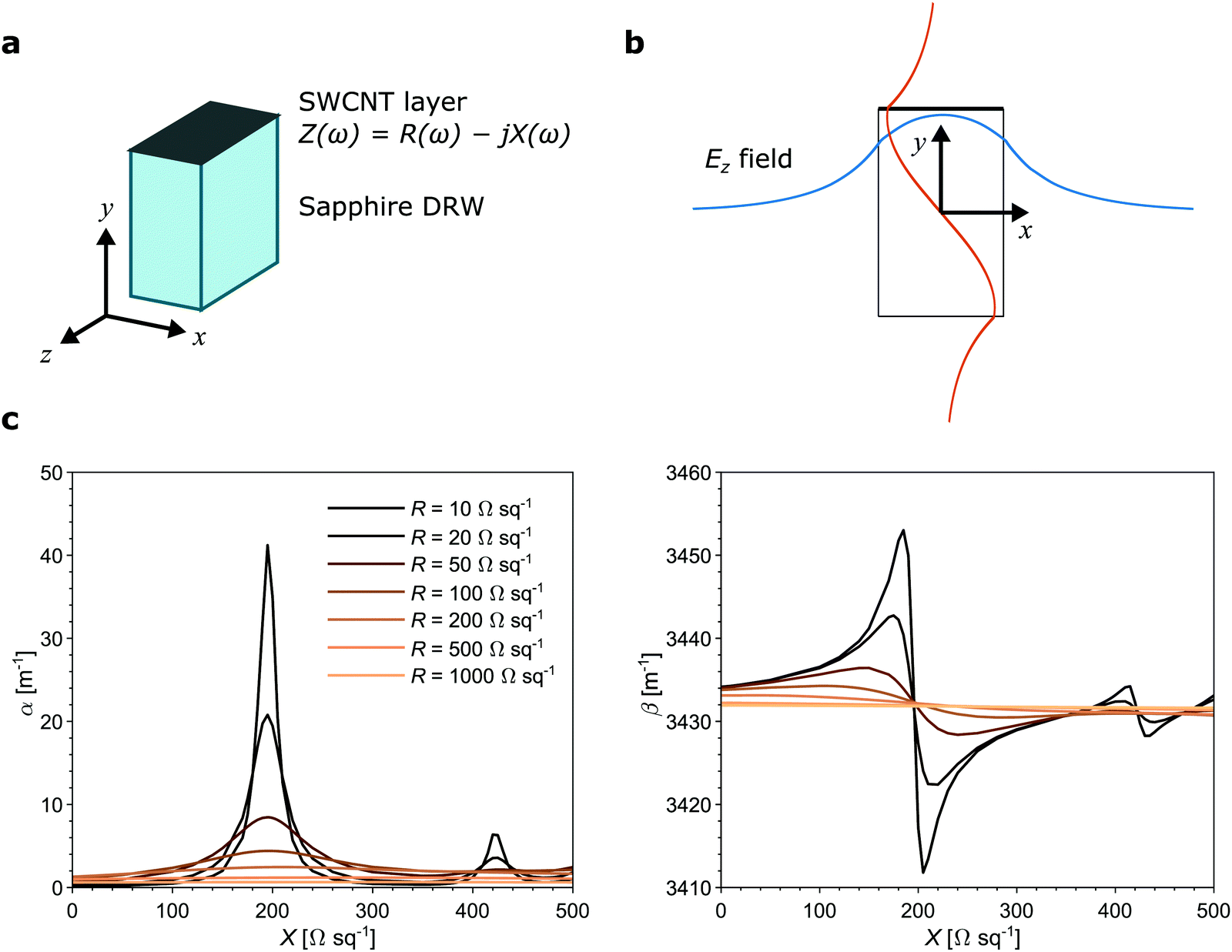 | ||
| Fig. 1 A single-walled carbon nanotube layer as a tunable impedance surface. (a) Schematic geometry of a sapphire dielectric rod waveguide (DRW), covered with a SWCNT layer that is modelled by a surface impedance Z(ω). (b) x and y amplitude distributions of the electric field Ez at 90 GHz in a DRW with a cross-section of 0.5 mm by 1 mm. The SWCNTs impact the propagation in the waveguide due to a strong evanescent field. (c) Simulated attenuation constant (α) and phase constant (β) of an electromagnetic wave propagating along the z axis at 90 GHz for varying surface impedance values. | ||
A resonance peak in the propagation constant is observed at X = 195 Ω sq−1. The amplitude and quality factor of the resonance are increasing for the decreasing values of R, while the resonance position is related to the cross-section geometry of the DRW. This is demonstrated by simulating a smaller rod with a 0.4 mm by 0.8 mm cross-section, where the resonance is shifted to X = 270 Ω sq−1 (see ESI, Fig. S2†). This geometry-dependent property signifies that different SWCNT layers can be adapted to a waveguide platform and scaled to other frequency bands. The resonance leads to high losses, represented by the peak in the attenuation constant, but it is also the source of an important variation in the phase constant. This can be used to create a phase shifting effect in the DRW by carefully selecting an impedance value in a zone of low attenuation combined with a steep slope in the phase constant.
Optically-controlled SWCNT-based phase shifters
Phase shifters were simulated and fabricated as single DRWs matched to standard metal waveguides by two tapering sections and covered on one side with SWCNT layers (see Fig. 2a and b). The layers were composed of randomly-oriented SWCNTs (see Fig. 2c) of mixed types, a mean nanotube diameter of 1.3 nm to 2 nm, and optical transparencies of 80% to 95%. Broadband simulations of the phase shifters were performed in the W-band for varying surface impedance values, which models the illumination of the SWCNTs. To quantify the phase shifter performance, we calculate the following figure of merit: FoM = phase shift/insertion loss. The simulated FoM at 90 GHz is given in Fig. S3† as a function of resistance and an optimized impedance value with respect to the FoM is chosen at R = 44 Ω sq−1. The resistance is then kept constant and the reactance is varied between X = 185 Ω sq−1 and X = 205 Ω sq−1 (corresponding to the largest β variation in Fig. 1c). The 10% increase in reactance is comparable to the measurements of a light-induced capacitance change in SWCNT layers.15 The simulation results are shown in Fig. 2d and Fig. S4.† The tuning of the surface impedance leads to a phase shift up to 1.5 deg mm−1, with an amplitude shift below 0.1 dB mm−1 in the whole frequency band. | ||
| Fig. 2 A SWCNT-based millimeter-wave phase shifter. (a) Schematic geometry of the phase shifter. The DRW is connected to two rectangular waveguide ports and is covered with a SWCNT layer that can be illuminated. (b) Image of the phase shifter measurement setup. (c) SEM image of the SWCNT network. (d) Simulated amplitude and phase shift with the SWCNTs modelled as an optically-tunable impedance surface with R = 44 Ω sq−1 and X varied between 185 Ω sq−1 and 205 Ω sq−1. (e) Measured amplitude and phase shift due to the illumination of SWCNT layers of different transparencies with varying light intensities. | ||
The corresponding fabricated phase shifters were measured in the W-band with a two-port measurement setup, while illuminating 2 cm-long SWCNT layers.17 The transmitted wave amplitude and phase shift, induced by the illumination, are shown in Fig. 2e for varying light intensities and SWCNT layer transparencies. By increasing the SWCNT layer's transparency up to 95% (corresponding to thinner layers), the transmission loss is improved with less than 0.2 dB amplitude variation in the measured frequency band. At the same time, a larger phase shift is observed with increasing illumination intensity, up to 15 degrees at 90 GHz and 23 mW cm−2. However, the dependence of the phase shift on the transparency seems marginal and layers with the lowest losses are therefore preferable in practice. The measured maximum phase shift corresponds to 0.75 deg mm−1, which is in relative agreement with the simulation results. The discrepancies are due to the manual application of the SWCNT samples, alignment of the DRWs to metal waveguides, and the supposition of constant impedance of the SWCNT layers with frequency, which exhibit resonant behavior in practice.30
Millimeter-wave beam steering
The SWCNT-based phase shifters were used as a reconfigurable element for optically-controlled millimeter-wave beam steering at 90 GHz. A DRW was covered with a thin SWCNT layer in a dual-rod antenna array, as shown in Fig. 3a. The nanotubes were modelled by a tunable impedance surface. The DRWs were fed by two hollow metal waveguides. The simulated radiation patterns of the antenna array without the SWCNT layer are given in Fig. 3b. The directivity of the array was improved with the increasing number of elements. Beam steering in the E-plane could be achieved by applying a phase shift ϕ between the adjacent excitation ports, as shown in Fig. 3c.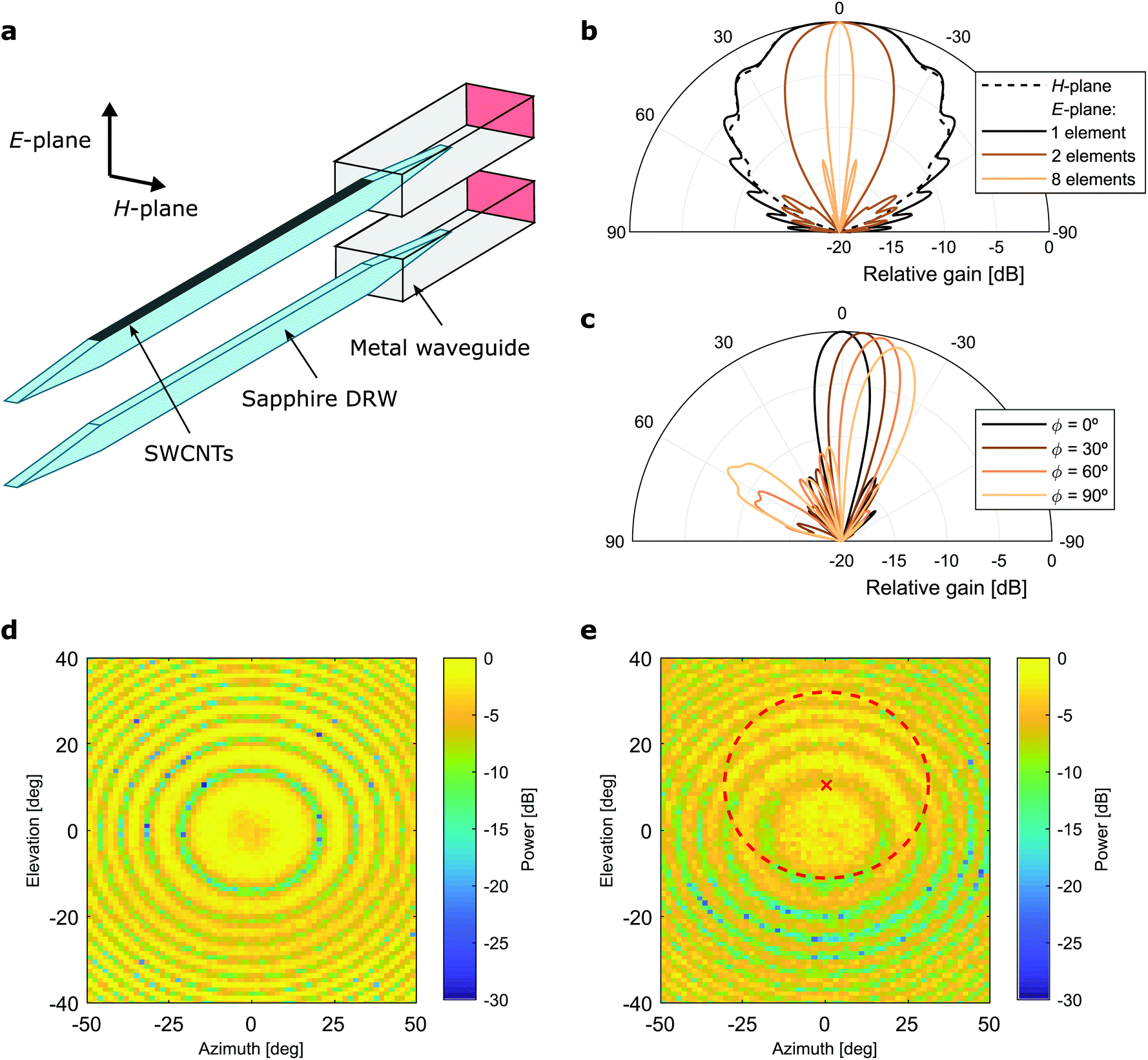 | ||
| Fig. 3 SWCNT-based beam steering at 90 GHz. (a) Schematic geometry of the two-antenna array. The DRWs are fed by rectangular waveguide ports. One of the rods is covered with a SWCNT layer, acting as a phase shifter under illumination. (b) Simulated radiation patterns in the E and H-planes for an increasing number of antenna elements. (c) Simulated beam steering in the E-plane for an increasing phase shift ϕ between adjacent elements. (d) A recorded radiation pattern of the two-antenna array in the initial state. (e) Measured beam steering due to the illumination of the SWCNTs. The red cross and the dashed circle are drawn as a guide to the eye to estimate the beam direction. | ||
The phase shift for beam steering could also be achieved by the optically-controlled SWCNT layer. An array of two DRW antennas corresponding to Fig. 3a was fabricated (see ESI, Fig. S5†). One of the antennas was covered with a thin SWCNT layer and illuminated. The radiation patterns were recorded without (Fig. 3d) and with illumination (Fig. 3e). A dominant interference pattern was seen due to a mismatch between the manually-aligned antenna elements during the measurement. Therefore, a red cross and a dashed circle were drawn as a guide to the eye to quantify the main beam direction. From the measurement results, a 10-degree spatial shift of the main beam was observed during illumination. The beam steering range and radiation pattern were comparable to that of the simulated one (see ESI, Fig. S6†).
Experimental
SWCNT sample characterization
The SWCNT layers used in this work were synthesized by aerosol chemical vapor deposition.14 The samples were characterized with a PerkinElmer UV-vis-NIR spectrophotometer at 550 nm. From the optical transmission measurements, the thickness of the SWCNT layers was estimated at 80 nm to 10 nm, corresponding to 60% to 95% transparencies.32 The optical absorbance spectrum of the SWCNTs is given in Fig. S7† with identified π-plasmon peak and peaks due to electronic transitions in metallic and semiconducting nanotubes. Scanning and transmission electron microscopy was performed with a high-resolution scanning electron microscope (SEM) JEOL JSM-7500FA at 2 kV and a spherical aberration corrected transmission electron microscope (TEM) JEOL JEM-2200FS at 80 kV. An average nanotube diameter of 1.3 nm to 2.0 nm was determined from S11 in the optical absorbance spectrum and TEM images. The SWCNTs were manually applied by direct dry transfer on the DRWs.Phase shifter measurement setup
The sapphire DRW was mechanically supported by a rigid Rohacell foam structure with a low dielectric constant and a low loss tangent. Sapphire was chosen as a pure dielectric, transparent in a wide range of visible and near-infrared light spectrum. The cross-section dimensions of 1.0 mm × 0.5 mm were chosen with 6 mm-long tapers, symmetrical in the E-plane.33 Two-port S-parameter measurements were performed with a Rohde & Schwarz ZVA-24 vector network analyzer with extension head modules in the W-band (75–110 GHz). The illumination inducing the phase shift was carried out with a tungsten halogen lamp with the main radiation spectrum at 550–680 nm with a light intensity of 23 mW cm−2, selected according to ref. 34 The incident optical power was determined with a “Sper Scientific 840011” laser power meter.Beam steering measurement setup
The array of the two DRW antennas was fabricated as shown in Fig. S5.† The antennas were fed by standard rectangular WR-10 waveguides through a power divider block.35 One of the antennas was covered with thin SWCNT layers and illuminated by the same tungsten halogen lamp as the phase shifter measurements. The radiation patterns were recorded at 90 GHz with a Rohde & Schwarz ZVA-24 vector network analyzer at a distance of 1 m.Conclusions
We demonstrate optically-controlled beam steering with an array of two dielectric rod antennas, one covered with a thin layer of SWCNTs. The nanotubes are used as a millimeter-wave tunable impedance surface under light illumination. The obtained steering range is approx. 10 degrees, limited by the generated phase shift due to the SWCNTs. Future investigations to enhance the effect are therefore considered, such as photo-sensibilization of SWCNTs by chemical functionalization36 and length-dependent resonance effects in individual nanotubes.16 This concept can be easily applied to antenna arrays with more elements to increase directivity.37 Moreover, the array can be expanded in the other plane for a full three-dimensional beam coverage, i.e. to achieve scanning in both E and H planes. Simplifying the feeding network by a dielectric one38 would reduce the complexity of the prototype, enabling a finer control over the spacing between the elements. Finally, fabricating the whole system as one, e.g. by micromachining,39 will among other things solve the mismatch problems. The design, with further proposed optimizations, has the potential to meet the large-bandwidth requirements of future millimeter-wave mobile communication components and opens a new direction for optically-controlled beam steering.Conflicts of interest
The authors declare no competing interest.Acknowledgements
This work was financially supported in part by the European Union's (EU) Horizon 2020 Innovative Training Network CELTA (grant no. 675683 of Call: H2020-MSCA-ITN-2015), by the European Research Council (ERC) under the European Union's (EU) Horizon 2020 research and innovation programme (grant no. 616846), and by the Foundation for Polish Science through grants TEAM/2016-3/25 and MAB/2018/9 under the Center for Terahertz Research and Applications (CENTERA) project, carried out within the ‘International Research Agendas’ programme co-financed by the European Union under the European Regional Development Fund.Notes and references
- Cisco, White Paper, 2017, 1454457600805266.
- D. Jiang and G. Liu, in 5G Mobile Communications, ed. W. Xiang, K. Zheng and X. Shen, Springer International Publishing, Cham, 2017, pp. 3–26, DOI:10.1007/978-3-319-34208-5_1.
- ITU-R_M.2370-0, IMT traffic estimates for the years 2020 to 2030, Geneva, 2015 Search PubMed.
- A. Fehske, G. Fettweis, J. Malmodin and G. Biczok, IEEE Commun. Mag., 2011, 49, 55–62 Search PubMed.
- C. X. Wang, F. Haider, X. Gao, X. H. You, Y. Yang, D. Yuan, H. M. Aggoune, H. Haas, S. Fletcher and E. Hepsaydir, IEEE Commun. Mag., 2014, 52, 122–130 Search PubMed.
- T. Do-Hong and P. Russer, IEEE Microw. Mag., 2004, 5, 57–67 CrossRef.
- T. S. Rappaport, S. Sun, R. Mayzus, H. Zhao, Y. Azar, K. Wang, G. N. Wong, J. K. Schulz, M. Samimi and F. Gutierrez Jr., IEEE Access, 2013, 1, 335–349 Search PubMed.
- M. Marcus and B. Pattan, IEEE Microw. Mag., 2005, 6, 54–62 Search PubMed.
- S. Kutty and D. Sen, IEEE Commun. Surv. Tut., 2016, 18, 949–973 Search PubMed.
- I. Uchendu and J. R. Kelly, Prog. Electromagn. Res., 2016, 68, 35–54 CrossRef.
- M. R. M. Hashemi, S.-H. Yang, T. Wang, N. Sepúlveda and M. Jarrahi, Sci. Rep., 2016, 6, 35439 CrossRef CAS PubMed.
- P. Avouris, M. Freitag and V. Perebeinos, Nat. Photonics, 2008, 2, 341–350 CrossRef CAS.
- D. Jariwala, V. K. Sangwan, L. J. Lauhon, T. J. Marks and M. C. Hersam, Chem. Soc. Rev., 2013, 42, 2824–2860 RSC.
- I. V. Anoshkin, A. G. Nasibulin, Y. Tian, B. Liu, H. Jiang and E. I. Kauppinen, Carbon, 2014, 78, 130–136 CrossRef CAS.
- S. Smirnov, I. V. Anoshkin, P. Demchenko, D. Gomon, D. V. Lioubtchenko, M. Khodzitsky and J. Oberhammer, Nanoscale, 2018, 10, 12291–12296 RSC.
- I. I. Nefedova, D. V. Lioubtchenko, I. S. Nefedov and A. V. Räisänen, IEEE Trans. Terahertz Sci. Technol., 2016, 6, 840–845 CAS.
- D. V. Lioubtchenko, I. V. Anoshkin, I. I. Nefedova, J. Oberhammer and A. V. Räisänen, 2017 IEEE MTT-S Int. Microwave Symp. (IMS), 4–9 Jun, 2017, pp. 1188–1191 Search PubMed.
- D. Lioubtchenko, S. Tretyakov and S. Dudorov, Millimeter-wave waveguides, Springer Science & Business Media, 2003 Search PubMed.
- C. Lee, P. Mak and A. DeFonzo, IEEE J. Quantum Electron., 1980, 16, 277–288 Search PubMed.
- D. Chicherin, S. Dudorov, D. Lioubtchenko, V. Ovchinnikov, S. Tretyakov and A. V. Räisänen, Microw. Opt. Technol. Lett., 2006, 48, 2570–2573 CrossRef.
- A. A. Generalov, I. V. Anoshkin, M. Erdmanis, D. V. Lioubtchenko, V. Ovchinnikov, A. G. Nasibulin and A. V. Räisänen, Nanotechnology, 2015, 26, 045201 CrossRef CAS PubMed.
- D. Wang, W. Zhao, H. Xie, J. Hu, L. Zhou, W. Chen, P. Gao, J. Ye, Y. Xu, H. Chen, E. Li and W. Yin, IEEE Trans. Nanotechnol., 2017, 16, 1132–1137 CAS.
- N. Ranjkesh, M. Basha, A. Taeb, A. Zandieh, S. Gigoyan and S. Safavi-Naeini, IEEE Trans. Terahertz Sci. Technol., 2015, 5, 268–279 CAS.
- K. Tsuruda, M. Fujita and T. Nagatsuma, Opt. Express, 2015, 23, 31977–31990 CrossRef CAS PubMed.
- D. Chicherin, M. Sterner, D. Lioubtchenko, J. Oberhammer and A. V. Räisänen, Int. J. Microw. Wirel. T., 2011, 3, 533–538 CrossRef.
- A. Rivera-Lavado, S. Preu, L. E. García-Muñoz, A. Generalov, J. M. de-Paz, G. Döhler, D. Lioubtchenko, M. Méndez-Aller, F. Sedlmeir, M. Schneidereit, H. G. L. Schwefel, S. Malzer, D. Segovia-Vargas and A. V. Räisänen, IEEE Trans. Antennas Propag., 2015, 63, 882–890 Search PubMed.
- P. Pousi, D. Lioubtchenko, S. Dudorov and A. V. Raisanen, 2008 38th European Microwave Conf., 27–31 Oct 2008, pp. 1082–1085 Search PubMed.
- A. A. Generalov, D. V. Lioubtchenko, J. A. Mallat, V. Ovchinnikov and A. V. Raisanen, IEEE Trans. Terahertz Sci. Technol., 2012, 2, 623–628 CAS.
- A. Rivera-Lavado, L.-E. García-Muñoz, A. Generalov, D. Lioubtchenko, K.-A. Abdalmalak, S. Llorente-Romano, A. García-Lampérez, D. Segovia-Vargas and A. V. Räisänen, J. Infrared, Millimeter, Terahertz Waves, 2017, 38, 33–46 CrossRef.
- S. Smirnov, I. V. Anoshkin, D. V. Lioubtchenko and J. Oberhammer, 2018 48th European Microwave Conf. (EuMC), 23–27 Sept., 2018, pp. 827–830 Search PubMed.
- J. Li, L. Hu, L. Wang, Y. Zhou, G. Grüner and T. J. Marks, Nano Lett., 2006, 6, 2472–2477 CrossRef CAS PubMed.
- I. V. Anoshkin, I. I. Nefedova, D. V. Lioubtchenko, I. S. Nefedov and A. V. Räisänen, Carbon, 2017, 116, 547–552 CrossRef CAS.
- D. V. Lioubtchenko, S. N. Dudorov and A. V. Raisanen, 2001 31st European Microwave Conf., 24-26 Sep., 2001, pp. 1–4 Search PubMed.
- S. Smirnov, I. V. Anoshkin, A. Generalov, D. V. Lioubtchenko and J. Oberhammer, RSC Adv., 2019, 9, 14677–14682 RSC.
- J. P. Pousi, D. V. Lioubtchenko, S. N. Dudorov and A. V. Raisanen, IEEE Trans. Antennas Propag., 2010, 58, 714–719 Search PubMed.
- I. V. Anoshkin, A. G. Nasibulin, P. R. Mudimela, J. Raula, V. Ermolov and E. I. Kauppinen, Carbon, 2012, 50, 4171–4174 CrossRef CAS.
- W. Withayachumnankul, R. Yamada, M. Fujita and T. Nagatsuma, APL Photonics, 2018, 3, 051707–051707 CrossRef.
- R. Reese, H. Tesmer, M. Jost, E. Polat, M. Nickel, R. Jakoby and H. Maune, J. Infrared, Millimeter, Terahertz Waves, 2018, 39, 1185–1202 CrossRef.
- S. Smirnov, A. Morales, C. Okonkwo, I. T. Monroy, D. V. Lioubtchenko and J. Oberhammer, 44th Int. Conf. on Infrared, Millimeter, and Terahertz Waves (IRMMW-THz), Paris, France, 1–6 Sept 2019, (accepted) Search PubMed.
Footnote |
| † Electronic supplementary information (ESI) available: Average atmospheric absorption of millimeter-waves (Fig. S1); a simulated propagation constant at 90 GHz for a sapphire DRW with a cross-section of 0.4 mm by 0.8 mm (Fig. S2); simulated figure of merit of the phase shifter at 90 GHz (Fig. S3); simulated S-parameters of a 10 mm long phase shifter (Fig. S4); beam steering measurement setup (Fig. S5); simulated radiation pattern of the two-antenna array with a layer of SWCNTs at 90 GHz (Fig. S6), and the optical absorbance spectrum of the SWCNT layer (Fig. S7). See DOI: 10.1039/c9nr02705j |
| This journal is © The Royal Society of Chemistry 2019 |