
 Open Access Article
 This Open Access Article is licensed under a Creative Commons Attribution-Non Commercial 3.0 Unported Licence
Fermi-level pinning in methylammonium lead iodide perovskites†
Thibaut
Gallet
 a,
David
Grabowski
b,
Thomas
Kirchartz
bc and
Alex
Redinger
*a
a,
David
Grabowski
b,
Thomas
Kirchartz
bc and
Alex
Redinger
*a
aScanning Probe Microscopy Laboratory, Physics and Materials Science Research Unit, University of Luxembourg, Luxembourg. E-mail: alex.redinger@uni.lu; Tel: +3524666446358
bInstitut für Energie- und Klimaforschung, Forschungszentrum Jülich GmbH, 52425 Jülich, Germany
cFaculty of Engineering and CENIDE, University of Duisburg-Essen, Carl-Benz-Str. 199, 47057 Duisburg, Germany
First published on 2nd September 2019
Abstract
Hybrid organic inorganic perovskites are ideal candidates for absorber layers in next generation thin film photovoltaics. The polycrystalline nature of these layers imposes substantial complications for the design of high efficiency devices since the optoelectronic properties can vary on the nanometre scale. Here we show via scanning tunnelling microscopy and spectroscopy that different grains and grain facets exhibit variations in the local density of states. Modeling of the tunneling spectroscopy curves allows us to quantify the density and fluctuations of surface states and estimate the variations in workfunction on the nanometre scale. The simulations corroborate that the high number of surface states leads to Fermi-level pinning of the methylammonium lead iodide surfaces. We do not observe a variation of the local density of states at the grain boundaries compared to the grain interior. These results are in contrast to other reported SPM measurements in literature. Our results show that most of the fluctuations of the electrical properties in these polycrystalline materials arise due to grain to grain variations and not due to distinct electronic properties of the grain boundaries. The measured workfunction changes at the different grains result in local variations of the band alignment with the carrier selective top contact and the varying number of surface states influence the recombination activity in the devices.
1. Introduction
The emergence of the hybrid organic–inorganic perovskites (HOIP) as absorber layers in thin film photovoltaics (PV) has led to an unprecedented boom of research in the community. While traditional thin film PV absorber materials had to be developed over several decades in order to reach power conversion efficiencies above 20%, the HOIPs have reached this milestone in only a couple of years.1 The material has ideal optoelectronic properties, such as a high absorption coefficient, a long minority carrier lifetime and a long minority carrier diffusion length combined with a tunable direct bandgap.1 Arguably the most remarkable property of lead–halide based solar cells is the high luminescence yield of films2 and photovoltaic devices3,4 and consequently the high open-circuit voltages reached relative to the thermodynamic limit.4 This ability to combine solution processing with low amounts of non-radiative recombination has not only allowed excellent open-circuit voltages but has also led to the situation that the efficiency of halide-perovskites has exceeded that of other polycrystalline thin-film solar cells such as CdTe and Cu(In,Ga)Se2. Recently efficiencies of 23% have been reported in ref. 5 with unpublished but certified results of 24.2% reported in the NREL efficiency table (compared to 23.35% for Cu(In,Ga)Se2![[thin space (1/6-em)]](https://www.rsc.org/images/entities/char_2009.gif) 6 and 22.1% for CdTe7).
6 and 22.1% for CdTe7).
For most semiconductors, different surface orientations with varying surface terminations, surface reconstructions and grain boundaries are potential regions of high non-radiative recombination, which reduces the maximum achievable open circuit voltage of the devices. Despite the exceptionally high power conversion efficiencies of the hybrid perovskites there is still a gap to the currently best performing single junction solar cells, which are all made from epitaxially grown GaAs.8 An important question is therefore if all of these polycrystalline technologies are suffering from the polycrystalline nature of the absorbers and/or of the grain boundaries.
In order to answer this question, it is important to investigate the electronic surface- and grain boundary-properties and to quantify the lateral variations in defect densities, workfunctions, bandgaps etc. In a subsequent step the origin of these fluctuations needs to be determined and the impact on device performance needs to be addressed. As typical grain sizes are in the sub-micrometer range, scanning probe microscopy (SPM) techniques are necessary to investigate the sample with nanometre resolution. Consequently, quite a number of reports have been published in the last years, where different SPM techniques have been used to study the perovskite surfaces (for a recent review see Ono et al.9). One of the major conclusions, drawn by most of the studies is that there are indeed variations of the optoelectronic properties on the nanometre scale. As discussed by Ono et al., it is necessary to establish a relationship between surface properties and bulk properties in order to fully understand how perovskites absorbers work in solar cells. Especially defects and surface states are of high importance for working devices, which will be discussed in the present work. Kelvin Probe Force Microscopy (KPFM) measurements show different workfunctions and surface photovoltages,10 conductive atomic force microscopy (AFM) measurements have shown inhomogeneous current collection within grains11 and at the grain boundaries12 and scanning tunnelling microscopy (STM) investigations suggest preferential segregation of PbI2 at the grain boundaries.13 Leblebici et al.14 observed facet-dependent variations of the photovoltaic efficiency. They speculated that the variations are due to locally varying trap state concentrations among crystal facets.
It also needs to be mentioned that, depending on the measurement conditions, ion migration due to strong tip sample interactions may be present15 and even deteriorate the sample surface while scanning. Finally, degradation is a central problem in all measurements, especially when the analysis is performed in ambient conditions.
Another interesting observation is that recombination rates and carrier lifetimes are changing from grain to grain as revealed from photoluminescence (PL) measurements.15–17 As PL measurements give direct access to the quasi-Fermi level splitting of the absorbers, these results corroborate that the variations on the micrometre scale are of central importance for high quality devices. The proposed origins of the fluctuations are chemical inhomogeneities,16 differences in trap densities15 and ion migration.17 The impact of grain boundaries is still under debate.
In this contribution we use scanning tunneling microscopy and spectroscopy (STS) to analyze the local fluctuations of the electronic properties on methylammonium lead iodide films. In contrast to all STM studies on perovskites in literature we combine our measurements with modeling of the spectra in order to quantify the number of surface states and the workfunction variations. We show that variations in the local dI/dV spectra cannot be directly linked to changes in the bandgap but an in-depth analysis, taking into account all the physical quantities that influence the tunneling current are mandatory for a correct interpretation of the experimental results.
2. Experimental details
In this study we analyse methylammonium lead iodide films grown by a standard solution based method with scanning tunnelling microscopy and spectroscopy in ultra-high vacuum. Details of the preparation method and of the experimental setup can be found in the ESI.† We focus on STM since this method gives direct access to the local density of states (LDOS) of the perovskite surface. Since the quality and homogeneity of the absorber surface is crucial for a good match between the perovskite and the extraction layers a direct measurement of the lateral variations of the LDOS is highly desirable and may unravel the magnitude of the lateral fluctuations in this material class. The extreme surface sensitivity and high spatial resolution of the STM enable us to study surface properties with nanometre precision. In order get reliable measurements all samples have been measured without air exposure prior to the STM analysis. We used an inert gas transfer from the glovebox to the SPM chamber in order to keep the surface contamination to a minimum and we probe the surface at room temperature where the material exhibits a tetragonal crystal structure. No bias light was used during the measurements in order to prevent light induced degradation in vacuum.18 An image of the investigated sample mounted on the sample holder plate is shown in Fig. 1 of the ESI.† The hybrid perovskites measured here exhibited a lifetime exceeding 100 ns at an injection level of approximately 3 × 10¹⁵ photons per cm3. These measurements have been done after the SPM measurements to corroborate that the absorber was still intact and the material did not deteriorate (see Fig. 2 in the ESI†). We do see a small shift in the PL peak position after storage of the sample in UHV for several months as discussed in more detail in the ESI (Fig. 3 ESI†). The XRD measurements do not show any indication of a secondary phase as shown in Fig. 4 of the ESI.†Before we proceed to the experimental results, a short introduction to scanning tunneling microscopy is necessary (for more details see for example ref. 19). A sharp metallic tip with a density of states ρt is brought in close vicinity d (d < 1nm) to the semiconducting surface with a density of states ρs. A tunneling junction forms and electrons tunnel from the sample to the tip or vice versa if a bias voltage V is applied. The tunneling current can be expressed as:20
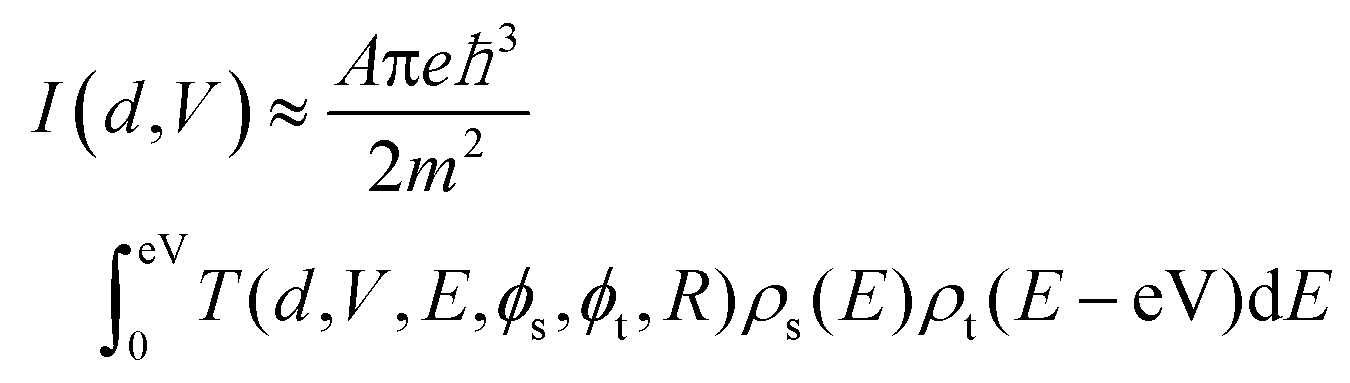 | (1) |
The transmission coefficient function T depends on the distance d, the applied voltage V, the radius R of the tip apex and the work functions φs,t of the tip and of the sample. Calculation of the derivative of the current with respect to voltage leads to a complicated term, which is usually simplified by assuming that the tip density of states ρt and the transmission coefficient T are constant. Under these conditions the tunnelling conductance can be approximated by
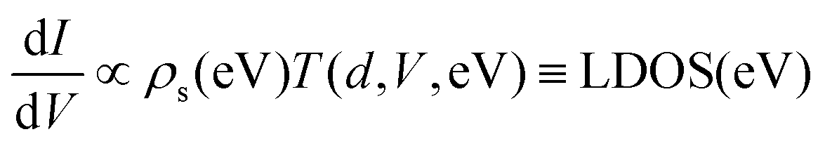 | (2) |
Due to the exponential voltage dependence of T the plotted dI/dV curve cannot be used to extract the bandgap. Therefore, the sample LDOS is often extracted via a normalization procedure, where in a first step the tunneling conductance dI/dV is normalized by I/V,21 which works well for metals. For semiconductors, where the dI/dV and the I/V functions vanish inside the semiconductor, the I/V needs to be broadened to prevent divergences at the band edges, denoted as  . This method has proven to be an effective way to determine the surface LDOS of semiconductors from which the surface bandgap in the absence of tip induced band bending can be extracted. However, care needs to be taken when analyzing polycrystalline materials since workfunction changes and bandgap variations may be confused. It is therefore intuitive to model the dI/dV curves in order to check the impact of all the different parameters on the resulting curve.
3. Results and discussion
In Fig. 1(a) a large area STM topography of the MAPI surface is presented. The surface consists of small grains with an average dimension of approximately 600 nm (as deduced from the standard deviation of the height-height correlation of the image, computed via the open source data analysis software Gwyddion). The surface is rather flat with an average RMS roughness of 15 nm for an average film thickness of 200 nm.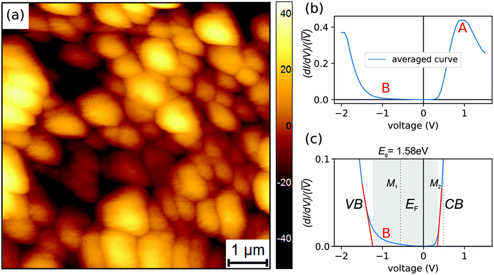 | ||
Fig. 1 (a) STM topography of the MAPI surface. Tunnelling parameters: I = 200 pA, V = −2 V, the colour bar indicates the height variations in nm. (b) Averaged  curve. The labels A, B denote the features that will be discussed further in the text. (c) zoom-in of (b) The band onsets are determined via extrapolation. The energetic positions M1 = −0.8 eV and M2 = +0.36 eV will be discussed later in the manuscript. VB and CB are the valence band and conduction band onsets. curve. The labels A, B denote the features that will be discussed further in the text. (c) zoom-in of (b) The band onsets are determined via extrapolation. The energetic positions M1 = −0.8 eV and M2 = +0.36 eV will be discussed later in the manuscript. VB and CB are the valence band and conduction band onsets. | ||
The average local density of states of the MAPI surface has then been extracted via current imaging tunnelling spectroscopy maps (CITS). In the present case a grid of 100 × 100 points is defined on the area of interest (in this case a 4 × 4 μm2 area (see Fig. 3(a)) which is a zoom in of Fig. 1(a)) and an I(V)-curve (−2 V to +1.5 V) has been measured for all the points of the grid at a set-point current of 200 pA. The average of the 10000 curves is presented in Fig. 1(b) and (c). In (b) the total normalized conductance is presented whereas in Fig. 1(c) only a zoom in of (b) is presented. We do observe several interesting features. First of all, we observe a well defined semiconducting gap and clear valence band (VB) and conduction band (CB) onsets. The Fermi-level position EF, given by the zero voltage position, suggests that the surface is n-type, which is in accordance with some of the photo-emission results presented in other reports.22,23 This interpretation is however only valid if we do not consider band bending, which alters the Fermi-level position at the surface compared to the one in the bulk. We will clarify the conductivity type at a later stage of the manuscript when the modelled dI/dV curves are discussed.
The results are not in agreement with scanning tunneling spectroscopy (STS) measurements by Azulay et al.24 where EF is closer to the valence band. Since the position of the Fermi-level depends on the ratio of the methylammonium halide to lead iodine composition,25,26 a possible explanation could be a different surface composition. Moreover, it has been shown that the workfunction and band bending at the surface of the perovskites are influenced by the underlying substrate.27 In the present case the perovskite absorbers were synthesized on ITO substrates in contrast to Azulay et al., where Au coated microscope slides were used.
In any case, we assert that the Fermi-level position measured with STM, on nominally the same material (CH3NH3PbI3) is not always the same, which corroborates that care needs to be taken when comparing measurements from different synthesis routes.
Extrapolation of the valence band and conduction band edges leads to a bandgap value of approximately 1.58 eV. This is in close agreement with the PL measurements, performed after the SPM measurements where a value of 1.6 eV has been deduced (see ESI†). However, we stress that the fitting range of the onsets is always subject to some ambiguity although the normalization procedure applied here helps to limit the error. We will perform a more elaborate evaluation later in this manuscript. As we will show, fitting of the dI/dV curves is especially important when laterally resolved data is analyzed in order to pinpoint the correct physical reasons to the variations in the onset of the conduction and valence bands. We observe a peak in the dI/dV curve at positive voltages, denoted as A in Fig. 1(b), which we attribute to the band structure of the MAPI. DFT calculations have shown a similar feature in the conduction band edge.28 Especially the vacant terminations of the (001) and (110) surfaces exhibit distinct peaks in the CB, which are attributed mostly to the projected density of states (PDOS) of the Pb-6p orbitals.28
A second feature is clearly visible in the negative voltage region denoted as B in Fig. 1(b and c). There is a much larger conductance in the tail region of the valence band compared to the conduction band. As we will show later in this manuscript, this feature is unevenly distributed over the surface of the perovskite and linked to different surface state densities.
In order to interpret the features visible in the STM, modelling of the dI/dV spectra is indispensable since the number of parameters that determine the conductance is large (cf.eqn (1)). Here, we use the formalism developed by Feenstra et al. for the case of III–V semiconductors. The method is described in detail in ref. 29 and references therein. In short, the theory consists of a 3D treatment of tip-induced band bending (TIBB) in the semiconductor combined with a planar configuration to model the tunnelling current based on the Bardeen approach.30 Especially the influence of surface states and their effect on TIBB can be modelled with this fitting routine. The method was very successful in explaining the impact of surface states on the tunnelling dI/dV spectra on GaAs(001). Here, we use the same fitting routine, which is freely available.31
In Fig. 2(a) the band diagrams of a n-type semiconductor and a metallic tip are sketched. Two situations are depicted. With no applied bias, the Fermi-levels are flat up to the surface in the absence of surface states. If a positive bias is applied to the tip (negative bias to the sample), an accumulation of electrons at the surface occurs due to TIBB. As described in detail by Feenstra et al., on a clean surface without intrinsic surface states TIBB at negative sample biases leads to a large amount of filled localized surface states, which dominate the conductance in the bandgap at low negative voltages in the dI/dV curves.
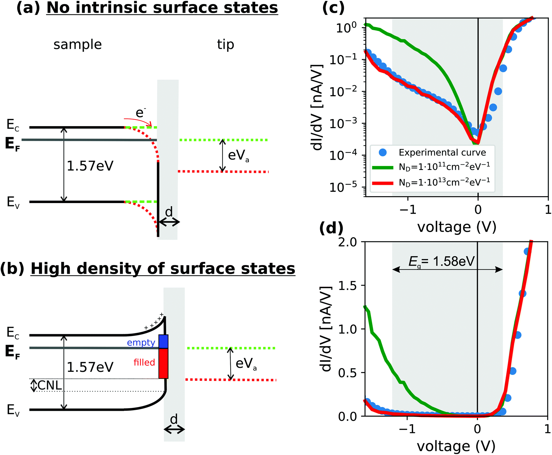 | ||
| Fig. 2 (a, b) Sketches of the tunnelling junction between the surface and the tip. The conduction and valence bands are denoted as EC and EV and the applied voltage is labelled as Va (green: no applied voltage; red: positive tip bias). (a) No intrinsic surface states, electron accumulation under applied voltage, illustrated by a downward band bending of EC, EV (from green to red). (b) High density of surface states with charge neutrality level (CNL) lower than the EF. Formation of acceptor type surface states and upward band bending. In case (b) there is no change of band bending due to applied voltage between the sample and the tip. (c), (d) Resulting simulated dI/dV curve on a logarithmic (c) and linear scale (d) for the two cases represented in (a), (b). ND denotes the defect densities used in the calculation. The shaded areas in (c), (d) correspond to the surface bandgap deduced in Fig. 1. The voltage on the x-axis in (c, d) corresponds to the voltage applied to the sample. | ||
In Fig. 2(b) a situation with a high density of surface states is sketched. The charge neutrality level in the present case is lower than the Fermi-level, which leads to negatively charged surface states. Since charge neutrality needs to be conserved in the semiconductor, upward band bending occurs, which is the usual situation for an n-type semiconductor. In this situation, the Fermi-level at the surface is pinned and no tip induced band bending occurs under an applied voltage.
The simulated dI/dV curves for the two situations are depicted in Fig. 2(c and d) on a logarithmic and on a linear scale. The curve with a low defect density (green line), the curve with the high defect density (red line) and the experimental curve (dotted curve) are shown.
Independent of the density of surface states, the calculated spectrum at positive sample voltages can be described in a satisfactory manner via an optimization of the contact potential difference between the tip and the sample, a realistic tip sample distance and the doping level in the bulk. In contrast, the fit at negative sample biases is poor and does not reproduce the experimental curve for a surface with low density of surface states. The conductance is too large in this case and the bandgap cannot be resolved. This is expected since on unpinned surfaces, the bandgap of a semiconductor can normally not be resolved due to TIBB.32
In contrast, a high surface defect density leads to strong Fermi-level pinning, which produces a lower tunneling conductance at small negative voltages. Only when the applied negative voltage is large enough, tunneling from the extended states of the valence band steps in. As shown in Fig. 2(c and d) the fit to the experimental data is much better.
In the present case we used a defect concentration ND = 1 × 10¹³ (cm2 eV)−1 located at 1.4 eV relative to the charge neutrality level (0.1 eV above the VB) and we used a Gaussian distribution of 135 meV. The most important parameters are presented in Table 1. Since the number of parameters necessary to calculate the conductance is large, we would like to discuss the results only on a qualitative level and do not imply that the used energy levels are accurately described down to a millivolt. We stress that the dip in the dI/dV-curves at small negative biases is only possible if we assume a small n-type bulk doping. For p-type doping the dip would show up at positive bias voltages. We use reasonable donor and acceptor binding energies and somewhat higher dielectric constant compared to conventional semiconductors. The results of the simulations are not very sensitive to these parameters. However, we stress that we need a high value of the surface states ND, which pins the Fermi-level, to have a good fit to the data. Before we discuss the origin of these surface states further we would like to investigate the lateral distribution of these surface defect densities in more detail since until now we only investigated the averaged dI/dV curve.
| Parameter | Value | Unit |
|---|---|---|
| Tip sample separation | 0.48 | nm |
| Tip radius | 16.5 | nm |
| Contact potential difference | −0.55 | V |
| Donor concentration | 1 × 10¹² | cm−3 |
| Bandgap | 1.57 | eV |
| Donor binding energy | 6 | meV |
| Acceptor binding energy | 28 | meV |
| Dielectric constant | 26 | |
| Temperature | 300 | K |
| Density of surface states ND | 1.3 × 10¹³ | cm−2 eV−1 |
| Charge neutrality level | 0.1 | eV |
| FWHM Gaussian distribution | 135 | meV |
| Centroid energies for the distribution | 1.5 | eV |
| Electron affinity of the sample | 4.07 | eV |
| FERMI energy of the tip | 5.0 | eV |
In Fig. 3 the laterally resolved dI/dV images are presented. Each image has been optimized to give the best possible contrast. We used a 3 × 3 averaging algorithm in order to remove some of the noise in the data. However, all the relevant features are already present in the raw data. In Fig. 3(a) the topography is depicted (a zoom-in of Fig. 1(a)) and the grain boundaries are marked with a black line in order to allow a better identification in the spectroscopic images. The lines mark the grain boundaries that are clearly visible and especially high symmetry grain boundaries may not show a topographic feature and consequently cannot be highlighted.33
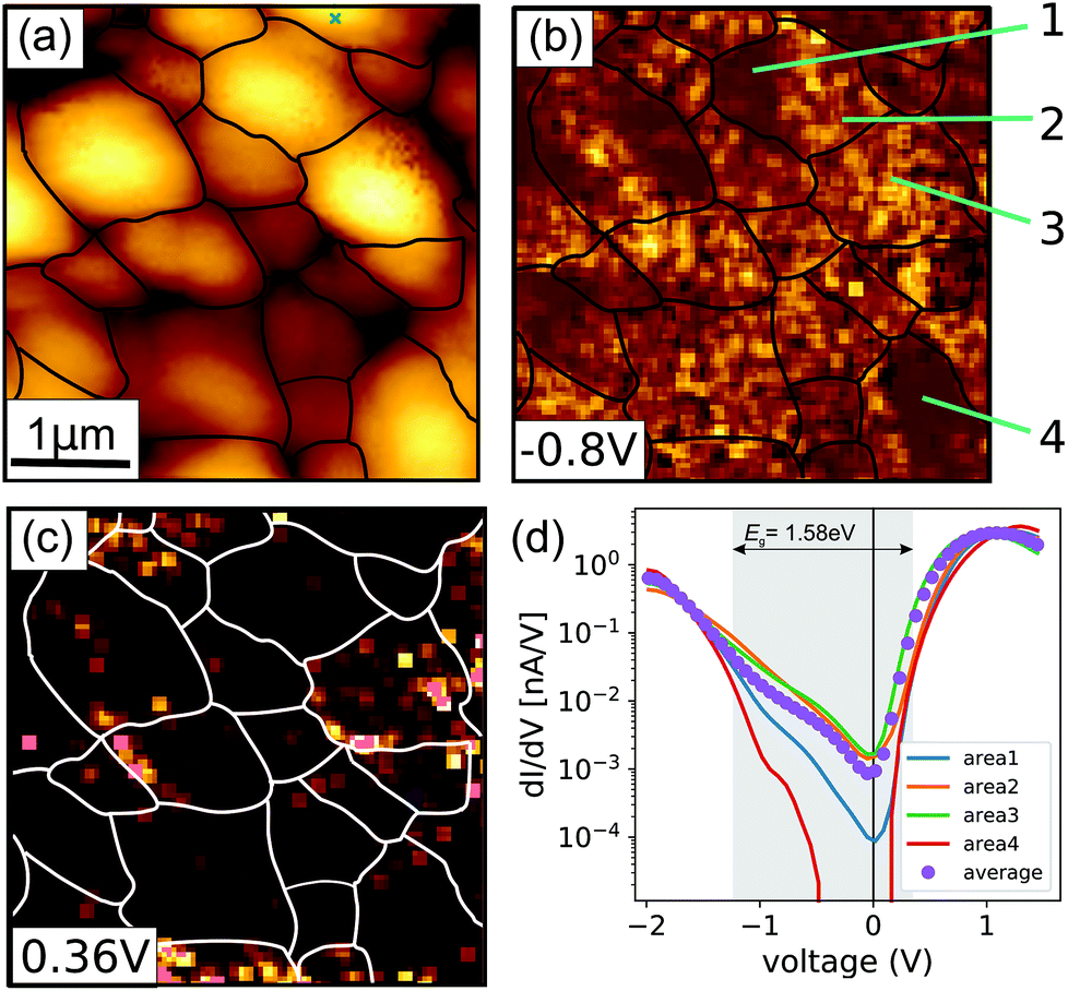 | ||
| Fig. 3 (a) STM topography acquired during the STS maps (this is an zoom in of Fig. 1(a). The black lines highlight the grain boundaries visible in the image. (b) Conductance map at −0.8 eV, (c) conductance map at +0.36 V. (d) Extracted dI/dV spectra for the grain regions highlighted in (b). | ||
In Fig. 3(b) a map at V = −0.8 V is shown, and in (c) a map at V = 0.36 V. These values have been chosen such that they match with the interesting features on Fig. 1(c) (labelled M1, M2). From Fig. 3(b) we can nicely see that the regions of high conductance are not at grain boundaries but within grains and that some of them exhibit substantial inhomogeneities, whereas some others are more homogeneous. To illustrate this we highlighted one grain with two different regions denoted as 1 and 2. These two regions, which exhibit clear differences in slope in the topographic image are different facets of the grain and they are distinct at a voltage of −0.8 eV. However, we also observe grains, which are homogeneous as for example grain 3. At positive voltages we do observe another interesting feature. The different contrasts in the regions 1,2 are not visible anymore. However, region 3 now has a much larger conductance than the regions 1,2, which was not the case at negative voltages. Region 4 is similar to region 1,2 where several facets are visible in the negative region, which disappear at positive voltages. The laterally resolved data shows that most of the changes in the tunnelling conductance are linked to different facets, which are certainly linked to different surface terminations. The different facets can be observed in line profiles along the grains, where the inclination angle changes. However, EBSD measurements need to be carried out on such samples in order to link the facets to a well defined crystallographic plane, which is very challenging due electron beam induced damage.
Theoretical calculations suggest that distinct surface terminations, with varying concentrations of surface states exhibit different magnitudes of charge carrier trapping, which determine non-radiative recombination rates.34 Our results corroborate these theoretical calculations that different surface terminations exhibit different amounts of surface states.
The dI/dV curves of the individual areas are summarized in Fig. 3(d), together with the average curve. Since the number of individual I(V) scans was much lower than in the averaged case, the dI/dV curves are smoothed. In agreement with the images we observe that there are substantial differences at the positive and negative regions of the dI/dV curves.
In the following we discuss how these changes can be understood. In Fig. 4 we present two sets of simulations. The starting parameters of the simulations are identical to the ones presented in Fig. 2 and Table 1. In Fig. 4 we vary (a) the contact potential difference (CPD) and (b) the defect density at the surface ND. In (a) the variation in the CPD illustrates a change of the workfunction of the sample, which is not induced by the surface states. The CPD is defined as the workfunction of the metallic tip minus that of the semiconducting sample divided by the elementary charge. As we can see, a variation of the CPD by 300 mV (from −0.65V to −0.35V) shifts the dI/dV curve at positive voltages to higher values and at negative voltages to more negative values. Moreover, the dI/dV curves are shifted to lower values (y-axis). We can conclude from this set of simulations that the CPD changes the onsets at both negative and positive sides however, the changes in both regions are similar in magnitude (in the bandgap region). If we compare these simulations with the experimental result we do see that at positive voltages the shift is small compared to the changes at negative voltages, where the dip in the dI/dV curve changes significantly. It can be concluded that a change in CPD alone cannot explain the observed experimental data. Therefore a second set of simulations has been performed where the defect density has been varied. As depicted in Fig. 4(b), we observe that the dip at negative voltages is changed but the region at positive voltages is not altered by the defect density. This makes sense since in the simulations the CPD and the defect densities are completely decoupled (two independent parameters). In experiment, however, a change in the defect density will also change the CPD via a change in the surface dipole. Another interesting observation in experiment is that at large negative voltages <−1.5 V there is a cross over between the curves. The ones with a stronger dip at −0.8 eV have a larger conductance at −1.5 eV. This behaviour is also visible in the simulations shown in Fig. 4(b) where the curves with a very high surface state density exhibit a larger conductance at far negative bias.
 | ||
| Fig. 4 Simulated dI/dV curves for (a) variations in CPD from −0.35 V to −0.65 V. In the region of the bandgap, the CPD changes the dI/dV curves symmetrically. (b) Variation in the defect density between 0 and 1 × 1014 cm−2 eV−1 for a constant CPD of −0.55 V. dI/dV curves are only affected at negative samples biases. | ||
From this set of simulations we do conclude that the observed changes in the dI/dV spectra are a direct consequence of a different amount of surface states, which in turn also influence the CPD value. The result clearly shows how important it is to do these high resolution measurements since most of the inhomogeneities are hidden within one grain or between different grains.
We have shown so far that the HOIP surface exhibits variations in the surface defect density. In the following we will first discuss, if these variations are due to a decomposed surface followed by a discussion of the grain boundary properties and possible origins of the observed facet dependent dI/dV contrast.
From our analysis we have deduced an average density of surface states, which is quite large and which induces Fermi-level pinning (see Fig. 2). If we use this average value of 1 × 1013 cm−2 eV−1 and use the Pb density on the (110) surface (3.7 × 1014 cm−2) we see that approximately 2.7% of these Pb atoms have to contribute to this surface defect density.
It has been shown that a high number of Pb0 at the surface leads to Fermi-level pinning18,35 and n-type doping. This high number of Pb0 surface states has only been observed with XPS on samples that were illuminated with light in UHV for a prolonged time. In our case we did not expose the sample to intense illumination and all our measurements have been performed in the dark. However, we had to expose the sample to a low intensity light illumination in order to be able to move the sample to the SPM and approach the tip to the sample. Consequently, we cannot completely rule out that there is an effect of light exposure.
The high density of Pb0 at the surface is attributed18,35,36 to metallic Pb, which is a direct consequence of a decomposition of the HOIP surface. In our case we cannot observe a massive change in the surface bandgap, which is a prerequisite for a large amount of PbI2 on the surface. Moreover, a large amount of metallic Pb is also inconsistent with our observations since the metallic lead should introduce a large amount of states in the bandgap (metallic behavior is expected). From this discussion we conclude that the origin of the facet dependent contrast is not likely to be due to a decomposed surface.
An additional effect to consider is that the samples were transferred from an inert gas glovebox to the SPM. Consequently the surface terminations may have been altered compared to single crystals cleaved in UHV.37 However, we stress that these nitrogen exposed surfaces are most relevant for solar cells, since most samples are prepared in inert gas gloveboxes. We therefore attribute the observed features to an intrinsic property of the HOIP surface, which is a direct consequence of different surface terminations, possibly modified by an exposure to N2.
So far we have only discussed the different facets of the polycrystalline grains. It is important to note that we do not see a distinct grain boundary contrast. In Fig. 5(a) a high resolution image of several grain boundaries is shown together with a dI/dV map at −0.6 V (Fig. 5(b)) and at +2 V (Fig. 5(c)). Interestingly, we do not observe variations in the grain boundary properties compared to the grain interior, which points towards an excellent passivation in these polycrystalline samples. This observation is not in accordance with most KPFM measurements performed in air or nitrogen filled gloveboxes (see for example ref. 9 and 11) where a distinct grain boundary contrast is visible, which can be altered by applied voltages or light. Currently, we can only speculate about the reason for this. As discussed extensively in this manuscript, STS is able to probe changes in workfunction. Since we do not see a contrast difference at the grain boundaries compared to the grains at high positive sample voltages, band bending can be ruled out. As our measurements have been performed under UHV conditions, where the moisture and oxygen levels are orders of magnitude lower than in a glovebox we attribute most of the contrast at the grain boundaries in the studies mentioned before to a residual moisture level which triggers decomposition and ionic mobility.
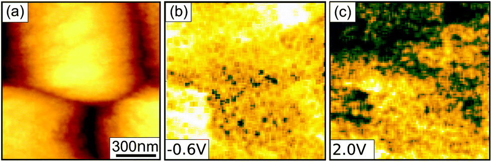 | ||
| Fig. 5 (a) High resolution STM topography. Tunnelling parameters: I = 200 pA, V = −2 V. (b) dI/dV conductance map at −0.6 V, (c), dI/dV conductance map at +2 V, no distinct grain boundary contrast visible. | ||
How do our results compare to other STM reports in literature? Our STS results extend the measurements by Azulay et al.24 who have only discussed the average density of states of the perovskites surfaces. Here, we show that electrical properties vary on the nanometre scale, which needs to be taken into account when discussing the recombination activity of the perovskite absorbers. Moreover, the discrepancy between the surface Fermi-level positions on nominally the same material shows that more fundamental studies are absolutely mandatory in order to better understand this material class. Another important aspect, which needs to be addressed is the contamination level of the absorbers. In the reports by Azulay et al.24 and Shih et al.13 it has not been specified if these samples were air exposed or not, which renders a direct comparison very challenging. Shih et al. have used the normalized dI/dV curves to extract variations in the bandgap. From our measurements and analysis it follows that such a simple evaluation cannot be done since the density of surface states and the workfunction alter the conduction and valence band onsets. We do not see any signatures of a phase segregation and we do not see a distinct grain boundary contrast in contrast to the work by Shih et al.
Finally, we discuss the most probable origin of the facet dependent contrast. Our results corroborate the speculations by Leblebici et al.14 and deQuilettes et al.16 that local variations of the surface defects are responsible for the observed intra grain variations. They found a correlation of the PL lifetime with local variations in the Cl/(Cl + I) concentration in the films. Our precursors also include chlorine and iodine and consequently this correlation could also be responsible for the observed changes in our study. Moreover, halide ions are known to selectively bind to crystal facets and induce changes in the electronic structure of semiconductors.38 We therefore assume that halide ions will play a key role in the observed variations of the surface state density and of the workfunctions. From our measurements we cannot directly observe changes in the halide concentration due to a lack of chemical sensitivity of the STM. We can rule out strong variations in the Cl/(Cl + I) ratio since this would lead to a change in the bandgap, which we would identify in the dI/dV map and via photoluminesence. Small variations (in the range of a few at%) cannot be resolved due to the finite energy resolution of the STM measurements (carried out at room temperature) combined with the variations in the workfunctions and surface state density, which alter the band edge onsets. In order to unambiguously corroborate that the changes in the facet contrast are due to distinct halide distributions, correlative STM and high resolution compositional measurements are necessary. Segregation in mixed halide perovskites have already been reported.16 However, it still needs to be clarified if individual facets have distinct concentrations of a single halide element (for example in pure iodine based perovskites) and if these variations are responsible for the variations in the dI/dV maps acquired in this study. The new insights with respect to the results by deQuilettes et al.16 are that we have quantified the number of surface states and the variations in workfunction, which may explain their findings, namely changes of the PL lifetime within individual grains.
The fluctuations on the nanometre scale impose another degree of complexity to the fabrication of the devices since (a) a suitable extraction layer needs to be used to passivate these states and the band alignment needs to be chosen such that enough selectivity is present despite the workfunction variations in the films.
Future experiments should focus on (a) determining the surface orientations with the lowest numbers of surface defects and (b) adapting growth conditions in a way to promote highly oriented growth where one type of facet dominates. Moreover, suitable extraction layers need to be developed, which reduce the number of surface states.
4. Conclusions
In conclusion, we have shown via scanning tunneling microscopy and spectroscopy that different surface terminations exhibit different amount of surface states, which leads to changes in Fermi-level pinning. The average surface bandgap is in good agreement with photoluminescence measurements, which is a direct consequence of Fermi-level pinning and the absence of tip induced band bending. Based on STS modeling we can furthermore identify significant variations in workfunction. Our results highlight that a simple extrapolation of the valence and conduction band onsets from the STS data to quantify bandgap variations is not correct if the number of surface states and the workfunction change on the nanometre scale. We do not see a distinct grain boundary contrast in the STS data, which rules out band bending between grain boundaries and grain interior in contrast to most KPFM measurements in air and in a nitrogen filled glovebox. Further comparative measurements with different SPM techniques are necessary to finally clarify the role of grain boundaries in these polycrystalline films. The lateral variations on the nanometre scale impose substantial difficulties for working solar cell devices since the band alignment also changes on the sub-micrometre scale. This needs to be taken into account when suitable selective contacts are deposited on top of the perovskite absorber material.Conflicts of interest
There are no conflicts to declare.Acknowledgements
TG & AR acknowledge financial support from the Fonds national de la recherche (“Sunspot”, Nr. 11244141). TK acknowledges support from the Impuls- und Vernetzungsfonds der Helmholtz Gemeinschaft via the project PEROSEED. TK and DG thank the Bavarian Ministry of Economic Affairs and Media, Energy and Technology for the joint projects in the framework of the Helmholtz Institute Erlangen-Nürnberg.References
- J. Berry, T. Buonassisi, D. A. Egger, G. Hodes, L. Kronik, Y. L. Loo, I. Lubomirsky, S. R. Marder, Y. Mastai, J. S. Miller, D. B. Mitzi, Y. Paz, A. M. Rappe, I. Riess, B. Rybtchinski, O. Stafsudd, V. Stevanovic, M. F. Toney, D. Zitoun, A. Kahn, D. Ginley and D. Cahen, Adv. Mater., 2015, 27, 5102–5112 CrossRef CAS PubMed.
- I. L. Braly, D. W. deQuilettes, L. M. Pazos-Outon, S. Burke, M. E. Ziffer, D. S. Ginger and H. W. Hillhouse, Nat. Photonics, 2018, 12, 472–476 CrossRef.
- M. Saliba, T. Matsui, K. Domanski, J. Y. Seo, A. Ummadisingu, S. M. Zakeeruddin, J. P. Correa-Baena, W. R. Tress, A. Abate, A. Hagfeldt and M. Grätzel, Science, 2016, 354, 472–476 CrossRef PubMed.
- Z. Liu, L. Krückemeier, B. Krogmeier, B. Klingebiel, J. A. Márquez, S. Levcenko, S. Öz, S. Mathur, U. Rau, T. Unold and T. Kirchartz, ACS Energy Lett., 2019, 4, 110–117 CrossRef CAS.
- Q. Jiang, Y. Zhao, X. Zhang, X. Yang, Y. Chen, Z. Chu, Q. Ye, X. Li, Z. Yin and Y. Jingbi, Nat. Photonics, 2019, 13, 460–466 CrossRef CAS.
- Solar frontier, Press release, January 21, 2019.
- M. A. Green, Y. Hishikawa, E. D. Dunlop, D. H. Levi, J. Hohl-Ebinger and A. W. Ho-Baillie, Prog. Photovolt., Res. Appl., 2019, 27, 3–12 CrossRef.
- B. M. Kayes, H. Nie, R. Twist, S. G. Spruytte, F. Reinhardt, I. C. Kizilyalli and G. S. Higashi, Proceedings of 37th Photovoltaic Specialists Conference, 2011, pp. 4–8.
- L. K. Ono and Y. Qi, J. Phys. Chem. Lett., 2016, 7, 4764–4794 CrossRef CAS PubMed.
- J. L. Garrett, E. M. Tennyson, M. Hu, J. Huang, J. N. Munday and M. S. Leite, Nano Lett., 2017, 17, 2554–2560 CrossRef CAS PubMed.
- J.-J. Li, J.-Y. Ma, Q.-Q. Ge, J.-S. Hu, D. Wang and L.-J. Wan, ACS Appl. Mater. Interfaces, 2015, 7, 28518–28523 CrossRef CAS PubMed.
- J. S. Yun, A. Ho-Baillie, S. Huang, S. H. Woo, Y. Heo, J. Seidel, F. Huang, Y. B. Cheng and M. A. Green, J. Phys. Chem. Lett., 2015, 6, 875–880 CrossRef CAS PubMed.
- M.-C. Shih, S.-S. Li, C.-H. Hsieh, Y.-C. Wang, H.-D. Yang, Y.-P. Chiu, C.-S. Chang and C.-W. Chen, Nano Lett., 2017, 17(2), 1154–1160 CrossRef CAS PubMed.
- S. Y. Leblebici, L. Leppert, Y. Li, S. E. Reyes-lillo, S. Wickenburg, E. Wong, J. Lee, M. Melli, D. Ziegler, D. K. Angell, D. F. Ogletree, P. D. Ashby, F. M. Toma, J. B. Neaton, I. D. Sharp and A. Weber-Bargioni, Nat. Energy, 2016, 1, 16093 CrossRef CAS.
- M. Yang, Y. Zeng, Z. Li, D. H. Kim, C.-S. Jiang, J. van de Lagemaat and K. Zhu, Phys. Chem. Chem. Phys., 2017, 19, 5043–5050 RSC.
- D. W. deQuilettes, S. M. Vorpahl, S. D. Stranks, H. Nagaoka, G. E. Eperon, S. H. J. Ziffer, E. Mark and D. S. Ginger, Science, 2015, 348, 683–686 CrossRef CAS PubMed.
- D. W. deQuilettes, W. Zhang, V. M. Burlakov, D. J. Graham, T. Leijtens, A. Osherov, H. J. Snaith, D. S. Ginger and S. D. Stranks, Nat. Commun., 2016, 7, 11683 CrossRef CAS PubMed.
- F. Zu, P. Amsalem, M. Ralaiarisoa, T. Schultz, R. Schlesinger and N. Koch, ACS Appl. Mater. Interfaces, 2017, 9, 41546–41552 CrossRef CAS PubMed.
- C. J. Chen, Introduction to Scanning Tunneling Microscopy, Oxford University Press, 2007 Search PubMed.
- C. Wagner, R. Franke and T. Fritz, Phys. Rev. B: Condens. Matter Mater. Phys., 2007, 75, 1–13 CrossRef.
- J. A. Stroscio, R. M. Feenstra and A. P. Fein, Phys. Rev. Lett., 1986, 57, 2579–2582 CrossRef CAS PubMed.
- J. Endres, D. A. Egger, M. Kulbak, R. A. Kerner, L. Zhao, S. H. Silver, G. Hodes, B. P. Rand, D. Cahen, L. Kronik and A. Kahn, J. Phys. Chem. Lett., 2016, 7, 2722–2729 CrossRef CAS PubMed.
- P. Schulz, E. Edri, S. Kirmayer, G. Hodes, D. Cahen and A. Kahn, Energy Environ. Sci., 2014, 7, 1377–1381 RSC.
- D. Azulay, I. Levine, S. Gupta, E. Barak-Kulbak, A. Bera, G. San, S. Simha, D. Cahen, O. Millo, G. Hodes and I. Balberg, Phys. Chem. Chem. Phys., 2018, 20, 24444–24452 RSC.
- Q. Wang, Y. Shao, H. Xie, L. Lyu, X. Liu, Y. Gao and J. Huang, Appl. Phys. Lett., 2014, 105, 163508 CrossRef.
- A. Zohar, I. Levine, S. Gupta, O. Davidson, D. Azulay, O. Millo, I. Balberg, G. Hodes and D. Cahen, ACS Energy Lett., 2017, 2, 2408–2414 CrossRef CAS.
- S. Olthof and K. Meerholz, Sci. Rep., 2017, 7, 1–10 CrossRef PubMed.
- J. Haruyama, K. Sodeyama, L. Han and Y. Tateyama, J. Phys. Chem. Lett., 2014, 5, 2903–2909 CrossRef CAS PubMed.
- N. Ishida, K. Sueoka and R. M. Feenstra, Phys. Rev. B: Condens. Matter Mater. Phys., 2009, 80, 1–8 Search PubMed.
- J. Bardeen, Phys. Rev. Lett., 1961, 6, 57–59 CrossRef CAS.
- R. M. Feenstra, SEMITIP, http://www.andrew.cmu.edu/user/feenstra/semitip_v6/.
- P. H. Weidlich, R. E. Dunin-Borkowski and P. Ebert, Phys. Rev. B: Condens. Matter Mater. Phys., 2011, 84, 1–8 CrossRef.
- R. Baier, C. Leendertz, D. Abou-Ras, M. C. Lux-Steiner and S. Sadewasser, Sol. Energy Mater. Sol. Cells, 2014, 130, 124–131 CrossRef CAS.
- H. Uratani and K. Yamashita, J. Phys. Chem. Lett., 2017, 8, 742–746 CrossRef CAS PubMed.
- Y. Li, X. Xu, C. Wang, B. Ecker, J. Yang, J. Huang and Y. Gao, J. Phys. Chem. C, 2017, 121, 3904–3910 CrossRef CAS.
- L. Wang, H. Zhou, J. Hu, B. Huang, M. Sun, B. Dong, G. Zheng, Y. Huang, Y. Chen, L. Li, Z. Xu, N. Li, Z. Liu, Q. Chen, L. D. Sun and C. H. Yan, Science, 2019, 363, 265–270 CrossRef CAS PubMed.
- R. Ohmann, L. K. Ono, H. S. Kim, H. Lin, M. V. Lee, Y. Li, N. G. Park and Y. Qi, J. Am. Chem. Soc., 2015, 137, 16049–16054 CrossRef CAS PubMed.
- S. Ghosh and L. Manna, Chem. Rev., 2018, 118, 7804–7864 CrossRef CAS PubMed.
Footnote |
| † Electronic supplementary information (ESI) available. See DOI: 10.1039/C9NR02643F |
| This journal is © The Royal Society of Chemistry 2019 |