
 Open Access Article
 This Open Access Article is licensed under a Creative Commons Attribution-Non Commercial 3.0 Unported Licence
Electrical and geometrical tuning of MoS2 field effect transistors via direct nanopatterning†
Fernando J.
Urbanos
 a,
A.
Black
b,
Ramón
Bernardo-Gavito
c,
A. L.
Vázquez de Parga
ad,
Rodolfo
Miranda
ad and
D.
Granados
*a
a,
A.
Black
b,
Ramón
Bernardo-Gavito
c,
A. L.
Vázquez de Parga
ad,
Rodolfo
Miranda
ad and
D.
Granados
*a
aIMDEA Nanociencia, C/Faraday, 9, 28049, Madrid, Spain. E-mail: daniel.granados@imdea.org
bInstitute for Physical Chemistry, University of Hamburg, Grindelallee, 117, 20146, Hamburg, Germany
cPhysics Department, Lancaster University, LA14YB, Lancaster, UK
dDep. Física de la Materia Condensada and IFIMAC, Universidad Autónoma de Madrid, Cantoblanco, 28049, Madid, Spain
First published on 30th May 2019
Abstract
Mechanically exfoliated van der Waals materials can be used to prepare proof-of-concept electronic devices. Their optoelectronic properties strongly depend on the geometry and number of layers present in the exfoliated flake. Once the device fabrication steps have been completed, tuning the device response is complex, since the geometry and number of layers cannot be easily modified. In this work, we employ Pulsed Focused Electron Beam Induced Etching (PFEBIE) to tailor the geometry and electronic properties of field effect transistors based on mechanically exfoliated Molybdenum Disulfide (MoS2) flakes. First, MoS2 field effect transistors are fabricated via optical lithography and conventional methods. Then, the geometry of the MoS2 source–drain conduction channel is modified employing a Xenon difluoride (XeF2) gas injection nozzle combined with a pulsed electron beam pattern-generation system. Electrical characterization of devices carried out before and after the nanopatterning step via PFEBIE reveals a shift in the doping from N-type towards P-type. We attribute this change to sulfur vacancies induced during the direct nanopatterning step. This is confirmed by micro-Raman and micro-Photoluminescence spectroscopy experiments. The direct nanopatterning method allows us to fine-tune the geometry and thus the electronic properties of the devices, once the conventional fabrication steps have been completed. The success rate of our tailoring method exceeds 85% when tuning the geometry of the flake into a 250 nm wide and straight conduction channel between source and drain.
Introduction
Transition metal dichalcogenides (TMDCs) such as molybdenum disulfide (MoS2), tungsten diselenide (WSe2) or tungsten disulfide (WS2) are considered ideal candidates for next-generation optoelectronic technologies.1–5 They consist of discrete two-dimensional (2D) layers bound together by weak Van der Waals forces. Atomically thin flakes can be easily exfoliated by the micromechanical exfoliation.6 These flakes exhibit distinctive thickness-dependent variations in their physical properties.7–10 The band structure of MoS2 varies with flake thickness, going from a 1.8 eV direct bandgap in a single layer (SL) to a 1.2 eV indirect bandgap in bulk.11,12 The SL semiconductor device exhibits unique optical properties, including strong photoluminescence (PL),13 valley polarization14,15 and strongly charged excitons.16Atomically thin MoS2 based transistors have been used to demonstrate new technologies, such as the fabrication of integrated circuits,17 RF electronics18 and flexible circuits.19 Nonetheless, the fabrication of optoelectronic devices from mechanically exfoliated MoS2 is an intricated process. In all cases, the geometry of the device is limited by the shape of the exfoliated flake, even when a deterministic stamping method is employed.20 The problem is also present when using CVD techniques. In this case, the material will grow in islands with reduced sizes and different orientations, hindering the device fabrication.21 For this reason, developing techniques to tailor the device geometry after the micro and nanofabrication steps have been completed is of interest. In the past, interacting electron and ion beams have been used combined with reactive gas mixtures to nano-pattern different substrates. Reactions of Si, SiO2 and Si3N4 substrates with XeF2, F2 and Cl2 gases under focused electron beams were experimentally studied.22 A similar approach was used with MoS2, placing it in a XeF2 atmosphere at high pressure and selectively patterning the material's geometry through a stencil mask prepared employing conventional lithography methods.23
In this work, we propose a variation of the Focused Electron Beam Induced Etching. We pulse the electron beam with a duty cycle while XeF2 is flowing towards the surface of the sample via a gas injection microneedle. The beam is scanned into a designed geometry employing a pattern generator. The proposed method allows us to modify the geometry of the conduction channel between source and drain of several field effect transistors fabricated out of exfoliated MoS2 flakes. Our method presents several advantages compared to those that use several fabrication steps, one being that it combines patterning and etching into a single step instead of having a two-step process as in previous studies.23 The second one is that it allows electronic and optical characterization before and after the tailoring step in a simple scheme.
Recent studies have shown the possibility of tuning the electrical properties of TMDC devices using helium ion beams.24–26 In these works, helium ion beams are utilized to tune the electrical properties of TMDCs by creating defects (i.e. vacancies, etc.) or changing their structural composition. Helium ion beam etching has also shown the viability of creating new geometries.27,28 For example, high-quality MoS2 ribbons down to 10 nm were fabricated to induce a change in the semiconducting phase of the material.27
One of the advantages of pulsed-focused electron beam induced etching (PFEBIE) compared with other studies is that the energy of the electron beam is much lower. In our case, the ebeam energy is 2.5 kV. Lower beam energies could reduce the damage in the sample and prevents from distortion of the MoS2 lattice. In addition, ion beam techniques are based on a physical method, similar to sputtering. Our technique is a chemical method, reducing the chances of damaging the samples, inducing amorphisation or electrically shortcutting into the device back gate.
In the same direction that in previous studies, the effect of this modification method on the electronic and optical properties of the FET devices has been studied employing room temperature current–voltage characterization, Atomic Force Microscopy, micro-Raman and micro-Photoluminescence. A clear heavily N-type doping towards intrinsic or lightly P-type doping shift is observed on the electronic I–V characteristic. This change is attributed to sulfur vacancies created when the etching was done. Spontaneous dissociation of fluorine causes the partial etching of the first sulfur layer in the TMDC structure. Optical properties are also altered due to the doping mechanism.
Results and discussion
Fig. 1a and b show an example of the patterning in a MoS2 FET. The initial width of the conduction channel between the source and the drain was 2.5 μm. After PFEBIE, the conduction channel was reduced into a 250 nm wide and straight wire. To simplify the behaviour and the data analysis, we only focus on wire-type geometries, but a variety of shapes can be achieved as shown in the ESI (Fig. S1†).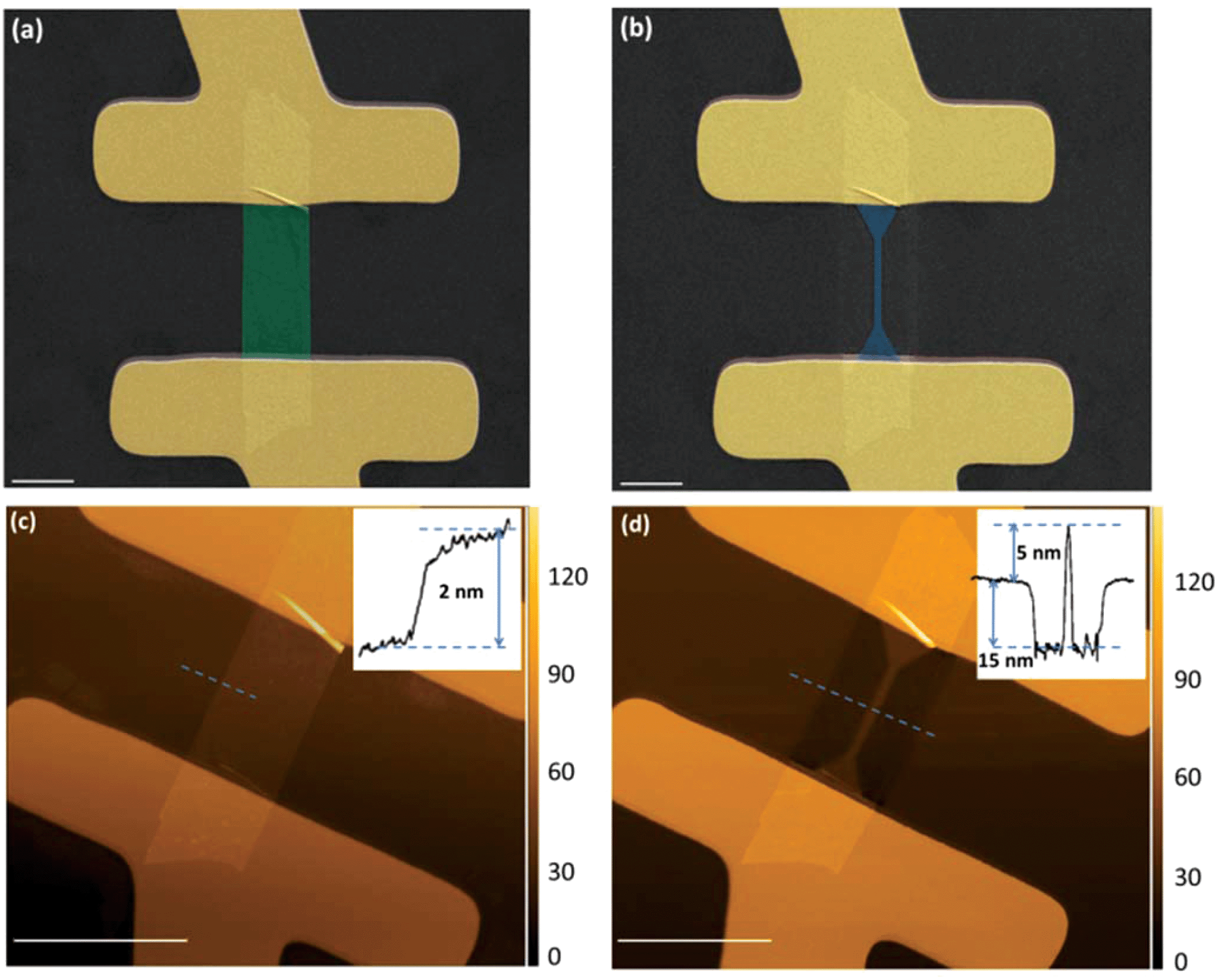 | ||
| Fig. 1 False-colour SEM images of a MoS2 FET device before and after the pulsed-FEBIE nano-patterning. (a) Original device showing a channel width of 2.5 μm. (b) Same device after reducing the conduction channel width by a factor of 10. Scale bars are 2 μm. (c) and (d) AFM images of the same device before and after the tailoring. The two insets show the profile at the same position before and after PFBEIE. Scale bars are 4 μm. | ||
Fig. 1c and d show AFM characterization of devices shown in Fig. 1a and b respectively. The insets represent the height profiles of the sample. Before PFEBIE the device thickness is 2 nm. Taking into account that the MoS2 monolayer is known to be around 0.7 nm thick,29 the device corresponds with a 2–3-layer initial flake. After the patterning, the thickness of the remaining MoS2 has increased to 5 nm. The profile shown in Fig. 1d also indicates that on the area exposed to the PFEBIE treatment, the SiO2 substrate is etched approximately 15 nm under these exposure conditions.
To study the origin of this increase in height we performed energy-dispersive X-ray spectroscopy (EDX) analysis before and after patterning as shown in Fig. S2.† M transition of gold is too near to Lα Mo transition. For this reason, Fig. S2† shows an exfoliated flake without gold electrodes to avoid overlap in the EDX signals of interest. The observable elements are the same between before and after steps, without any fluorinated signal. It indicates that there is no signature of deposition of any by-product material or fluorinated compounds. It seems that this height increase can be attributed to redeposited Mo or S species. In case the material would be redeposited, it has a similar grain structure than the previous one and is not possible to observe any clear change by EDX or AFM. Additional backscattered electron (BSE) imaging was performed before and after the patterning in another device as shown in Fig. S3.† BSE detector also gives information about the composition of the material. Fig. S3† shows that the contrast remains equal between before and after steps, showing that the composition of the device did not change within the resolution limit of our BSE detector. The origin of this height increase remains unclear and further studies will be carried out to clarify this point in future studies.
Fig. 2a displays the electric response under gate sweeping before and after PFEBIE in the MoS2 device shown in Fig. 1. The red curve corresponds to the initial device, where a strong N-type behaviour is observed, with the threshold voltage at −90 V, calculated with the extrapolation in the linear region method as reported in reference.33 N-Type doping is mostly reported in literature for FET devices fabricated out of mechanically exfoliated bulk MoS2 minerals.34 The field effect transistor works after the nano-patterning step. It is also important to mention that despite the oxide etching, the device does not show gate leaks, as shown in Fig. 2. After PFEBIE the threshold voltage value of 2 V indicates that the devices’ N-doping has been reduced, becoming more intrinsic. This change in doping is present in the non-exposed regions of the remaining MoS2 material. This suggests that a XeF2 fraction spontaneously dissociates when free radicals interact with the surface, causing sulfur etching on the unexposed areas. In a spontaneous etch process, the chemical reactions proceed partially without the need for activation by ebeam bombardment.35,36
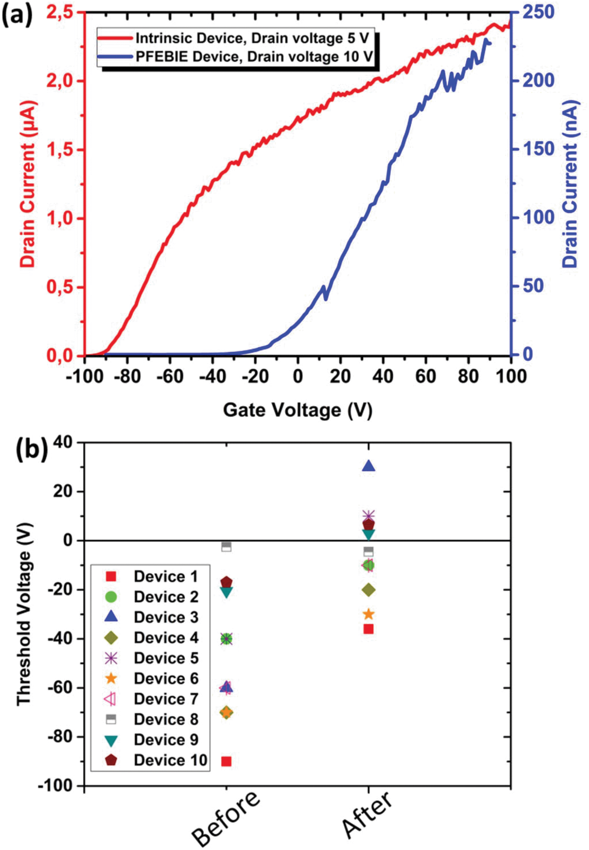 | ||
| Fig. 2 (a) Room temperature transfer characteristics of the FET device shown in Fig. 1 before (red) and after (blue) the nano-patterning. The threshold voltage variation indicates a shift from N-type doping to intrinsic doping after PFEBIE. In this case the threshold voltage varies from −90 V to 2 V. (b) Shift in the threshold voltage of ten different devices before and after the channel width tailoring. | ||
In the initial device, the OFF, ON and saturation states of the transistor can be clearly identified. However, after PFEBIE, due to the change in the doping, the saturation state is not clearly observed because it is beyond the safe gate voltage measuring range, since higher gate bias would induce the dielectric rupture of the SiOx insulating layer. It also is important to mention that there is a large decrease in the current after the patterning. The initial device is in the μA regime while the patterned device is in the nA range. This is a consequence of a decrease in the channel width after PFEBIE, which should reduce the current to approximately 10% its initial value. For a given Vds the initial device is nearly in the ON state at Vg = 0 V, while the after device is nearly in the off state for the same Vds and Vg set-points. This makes comparison hard between before and after devices (see ESI†). Additional electrical characterization is shown for a different device in Fig. S5.†
The original device has a mobility of 1.96 cm2 V−1 s−1, within the standard values of these type of devices.6,17 After PFEBIE, the mobility was reduced to 0.39 cm2 V−1 s−1. The change in the mobility is caused by changes/defects in the final channel. The ON/OFF ratio of the original device was 105. After the nano-patterning this ratio was not possible to be calculated because the saturation region is not observable. Calculations and more details about mobility and ON/OFF ratio are discussed in the ESI.†
To study the doping mechanism, electrical measurements were performed in 10 different devices, before and after the PFEBIE patterning. Fig. 2b shows the value of the threshold voltage in all samples before and after PFEBIE. We observe that 90% of them show a change from N-doped towards intrinsic or even lightly P-doped manifesting a general tendency in the electrical behaviour. The mechanism is not totally clear, but a possible hypothesis to that tendency is that sulfur vacancies are created in the unexposed regions when XeF2 etches the desired zones.37–39 It is well known that sulfur vacancies are a strong p-dopant due to a charge transfer mechanism in sulfur deficient MoS2,40,41 making this vacancy process a plausible scenario. Some groups have studied the interaction of TMDCs with helium ion beams, observing the creation of vacancies,25,28 what supports our hypothesis.
Different studies have reported a phase change from semiconductor (2H phase) to metallic (1 T phase) in MoS2 devices under plasma treatment.30 Due to the metallic character of the 1T MoS2 phase,31,32 it would not show any gate response in the electrical characterization. In our case, under gate sweeping, the device is still clearly showing a field effect response after PFEBIE, showing the characteristic behavior of the semiconducting 2H phase.
As Fig. 2b shows, a larger dispersion in the threshold voltage of the studied devices is observed before the patterning. The mean value of the threshold voltage before the patterning is Vth = 47 ± 30 V. After the patterning it is Vth = −7 ± 20 V. The dispersion in the Vth of the original devices is mostly attributed to the differences in the shape, number of contacted layers or total area covered by the metallic contacts. All of them are parameters impossible to control with high accuracy with the method employed to fabricate the devices. For that reason, it is complex to determine a standard conduction channel in the fabrication procedure. The power of PFEBIE resides on controlling the channel width and its geometry. After the patterning, the channel can be standardized and in this work all the channels in the after-devices are 250 nm wide, as Fig. S4† shows. This clearly reduces the dispersion of the threshold voltage after the patterning procedure. Nonetheless, some of the geometrical factors mentioned above remain unaffected after the PFEBIE patterning process, i.e. the area under the source–drain contact electrodes. These factors affect the device performance and thus the FET results after the patterning still exhibit some dispersion.
In order to validate our sulfur vacancy hypothesis we have performed optical characterisation of the devices before and after the tailoring step. The Optical properties of MoS2 flakes, such as Raman and PL, are also strongly dependent on the doping level and sulfur vacancies.42–44 Micro-PL on MoS2 flakes has two characteristic features, the A and B excitons, that appear as a consequence of the band splitting due to spin–orbit coupling.13Fig. 3 shows PL maps before and after the etching process of the device shown in Fig. S4i.† The darker horizontal bars correspond with the Cr/Au electrodes. Although it does not affect optical measurements, the metallic character of the electrodes produces a higher Rayleigh scattering of the laser in those zones, increasing the background signal in those regions with respect to the substrate. This creates a ghost image of the electrodes arising from a background difference rather than from a true Raman Signal at the given energy of the map. Fig. 3a and b correspond respectively to the intensity maps of the MoS2 A and B excitonic transitions before PFEBIE. The inset of Fig. 3a shows that the A transition occurs at 675 nm and the B transition at 625 nm. Fig. 3c and d displays the same features after PFEBIE, where the narrowed MoS2 channel is clearly seen. The channel was patterned in a cross-bar shape to avoid electrical conductivity out of the 250 nm wire (see ESI†). A blue-shift of approximately 10 nm (average taken from different points present in the map) is observed for both excitons, as seen in the inset of Fig. 3c.
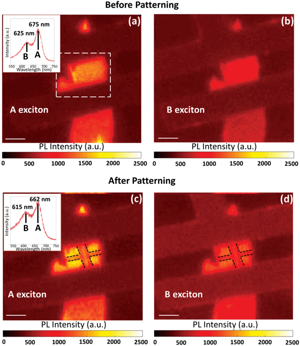 | ||
| Fig. 3 Photoluminescence maps before and after the patterning process. (a), (b) A and B exciton maps of the device before the patterning. The inset shows the photoluminescence spectrum before PFEBIE where A and B excitons can be identified. (c), (d) A and B exciton maps after the patterning, where the 250 nm narrowing can be clearly observed. The inset represents the PL spectrum after PFEBIE. A blue-shift of 10 nm is observed for both exciton peaks. Scale bars are 2 μm. | ||
The relative intensity of the excitonic transitions also changes after the patterning. The initial device shows an IA/IB ratio of 1.40, where IA and IB are the intensity of the A and B transitions respectively. After PFEBIE the intensity ratio is 1.25. This change in the exciton intensity ratio is attributed to the doping changes observed, in good agreement with previous studies,41,45 where chemical doping over MoS2 devices result in a more intense IB because of the p-doping effect.
In addition to PL characterization, Raman spectroscopy was performed. MoS2 has two characteristic Raman modes. The A1g mode corresponds with an out of plane vibration of sulfur atoms. The other mode, which is called E12g, corresponds with an in-plane shear mode of both, Mo and S atoms. Intensity maps shown in Fig. S7† reveal that after PFEBIE Raman peaks are still present. It indicates that the device has not been chemically altered substantially.
Fig. 4 shows Raman maps corresponding to the zoom of the dashed zone displayed in Fig. 3a. Fig. 4a and b correspond to the peak position difference (PPD) between the E12g and the A1g peaks before and after PFEBIE respectively. An increase of almost 2 cm−1 (average taken from different points of the flake) is identified.
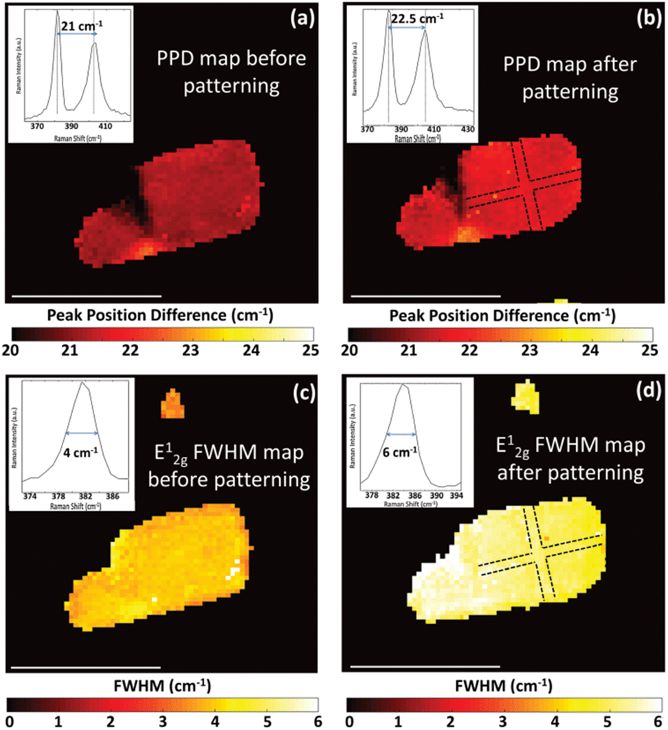 | ||
| Fig. 4 Zoom taken from the dashed square zone in Fig. 3a. Dashed lines in (b) and (d) show the new channel after the patterning. The channel is not visible due to fitting parameters. (a) PPD mapping before PFEBIE. Inset corresponds with a Raman spectrum indicating the average of the PPD (taken from different points of the flake). (b) PPD mapping after PFEBIE. The inset represents a Raman spectrum with the PPD average. An increase of 2 cm−1 can be identified. (c) E12g full width at half maximum (FHWM) mapping before PFEBIE. (d) E12g FWHM mapping after PFEBIE. An increase of 2 cm−1 is observed after the patterning. Scale bars are 2 μm. | ||
Fig. 4c and d represent the evolution of the E12g full width at half maximum (FWHM) before and after PFEBIE, showing an increase from 4 cm−1 to 6 cm−1 on average. Dashed marks indicate where the narrowing was done. Due to fitting parameters the narrowing cannot be clearly observed. By changing the scale, the patterning can be seen, but information about the surrounding environment will be missed. It is important to mention that the same behaviour is observed after A1g FWHM analysis as Fig. S6† reveals. Spontaneous dissociation of XeF2 may change the sulfur content and therefore doping of the unexposed regions. These phenomena may change the Raman signal, showing a similar transition as previously reported.44
Conclusions
The experiments here reported have shown that PFEBIE is a tool that allows tailoring device geometries after lithographical fabrication processes without the need of a stencil mask, saving fabrication steps and possible contaminants.The AFM characterization shows a change in the height profile of the device, indicating that there might be some intercalated etchant, or material deposition on the device surface.
Transport characterization has revealed a transition from N-type doping to intrinsic or even P-type doping after PFEBIE. This is attributed to sulfur vacancy creation after the etching process. A study of 10 devices has been carried out, showing that there is a clear tendency in the doping change. Thereby this technique could show the viability of tailor the electric behaviour once a device has been electrically characterized.
The sulfur vacancy hypothesis is supported by micro-Raman and micro-PL spectroscopy. Regarding PL spectroscopy, we have observed a change in the relative IA/IB ratio due to the doping mechanism It is also possible to observe a blue-shift in the excitonic transitions of 10 nm. It is important to mention that the Raman intensity mapping evidences that, despite these changes in doping and electric behaviour, both peaks are still present, so we can conclude that the device has not been substantially chemically altered.
Experimental section
MoS2 flakes were exfoliated onto a degenerate p-doped silicon wafer capped with a 285 nm SiO2 layer. Electrodes were patterned using direct write laser optical lithography, followed by thermal evaporation of chromium (10 nm) and gold (70 nm), resulting in a back-gated field effect transistor geometry. After photoresist liftoff, an annealing was performed in an argon/hydrogen atmosphere at 300 °C to remove resist residues and decrease contact resistance. Back-gate electrical transport characterization was done using a Keithley 4200 Probe Station.Scanning Raman and PL mappings were carried out at room temperature using a 488 nm Argon laser as excitation source, a dichroic and razor edge filters and a 40× 0.65 NA objective in a 0.5 m spectrometer with a 1200 lines per mm diffraction grating. The optical setup is coupled to a piezo-electric scanner that allows the acquisition of spectroscopic mappings. 100 × 100 pixel mappings were obtained with an acquisition time of 1 s per pixel.
Following the initial characterization of the devices, PFEBIE nano-patterning was used to alter device geometries. This method consists of the combination of a pulsed electron beam and a micro gas injection system, carried out within a Scanning Electron Microscope chamber. The gas (XeF2) enters the chamber through a small nozzle and adsorbs on the device surface. The electron beam is then pulsed and scanned over the device surface. The focused electron beam plays an important role, dissociating the gas mixture into fluorine and creating the desired geometries. The beam energy and current were 2.5 kV and 0.24 nA respectively. The aperture size was 30 μm. The nozzle is placed 250 μm above the desired area. It has a size of 500 μm width and 500 μm height. The base vacuum is 10−7 mbar and raises to 10−4 mbar when the gas is flowing. The reservoir temperature is set at 10 °C. A 16 bit per channel pattern generator, 400 MHz Raith multibeam is employed to define the new geometries, with 250 loops and a dwell time of 500 ns. With these parameters, the fabrication time per tailored device is around 2 minutes. After PFEBIE nano-patterning, the devices were characterized again by electrical measurements, AFM microscopy, and spectroscopic techniques such as Raman and PL.
EDX measurements were taken into a High definition SEM (EVO-HD from Carl-Zeiss) equipped with a Peltier cooled EDS detector (Xflash 430 from Bruker), with 30 mm2 detector area, 133 eV resolution and a working temperature of 40 K.
Conflicts of interest
There are no conflicts to declare.Acknowledgements
This work is partially supported by the Spanish Ministry of Economy, Industry and Competitiveness through Grant DETECTA ESP2017-86582-C4-3-R and the Comunidad de Madrid through Grant S2018/NMT-4291 TEC2SPACE-CM. D. G. acknowledges Grant RYC-2012-09864. A. L. V. P. acknowledges the Ministerio de Economía y Competitividad (MINECO) project FIS2015-67367-C2-1-P. A. B. acknowledges Graphene Core Grant H2020-FETFLAG-2014. IFIMAC acknowledges support from the “María de Maeztu” Programme for Units of Excellence in R&D (MDM-2014-0377). IMDEA Nanociencia acknowledges support from the ‘Severo Ochoa’ Programme for Centres of Excellence in R&D (MINECO, Grant SEV-2016-0686). The authors also want to acknowledge Dr Jorge Trasobares and Victor Marzoa for fruitful scientific discussions.Notes and references
- B. Liu, A. Abbas and C. Zhou, Adv. Electron. Mater., 2017, 3, 1700045 CrossRef.
- C. Gong, Y. Zhang, W. Chen, J. Chu, T. Lei, J. Pu, L. Dai, C. Wu, Y. Cheng, T. Zhai, L. Li and J. Xiong, Adv. Sci., 2017, 4, 1700231 CrossRef PubMed.
- H. Tian, M. L. Chin, S. Najmaei, Q. Guo, F. Xia, H. Wang and M. Dubey, Nano Res., 2016, 9, 1543–1560 CrossRef CAS.
- Q. Zeng and Z. Liu, Adv. Electron. Mater., 2018, 4, 1700335 CrossRef.
- K. F. Mak and J. Shan, Nat. Photonics, 2016, 10, 216 CrossRef CAS.
- K. S. Novoselov, D. Jiang, F. Schedin, T. J. Booth, V. V. Khotkevich, S. V. Morozov and A. K. Geim, Proc. Natl. Acad. Sci. U. S. A., 2005, 102, 10451 CrossRef CAS PubMed.
- J. Choi, H. Zhang and J. H. Choi, ACS Nano, 2016, 10, 1671–1680 CrossRef CAS PubMed.
- X. Huang, Z. Zeng and H. Zhang, Chem. Soc. Rev., 2013, 42, 1934–1946 RSC.
- D. Kufer and G. Konstantatos, Nano Lett., 2015, 15, 7307–7313 CrossRef CAS PubMed.
- S. Najmaei, M. Amani, M. L. Chin, Z. Liu, A. G. Birdwell, T. P. O'Regan, P. M. Ajayan, M. Dubey and J. Lou, ACS Nano, 2014, 8, 7930–7937 CrossRef CAS PubMed.
- K. K. Kam and B. A. Parkinson, J. Phys. Chem., 1982, 86, 463–467 CrossRef CAS.
- K. F. Mak, C. Lee, J. Hone, J. Shan and T. F. Heinz, Phys. Rev. Lett., 2010, 105, 136805 CrossRef PubMed.
- A. Splendiani, L. Sun, Y. Zhang, T. Li, J. Kim, C.-Y. Chim, G. Galli and F. Wang, Nano Lett., 2010, 10, 1271–1275 CrossRef CAS PubMed.
- K. F. Mak, K. He, J. Shan and T. F. Heinz, Nat. Nanotechnol., 2012, 7, 494 CrossRef CAS PubMed.
- H. Zeng, J. Dai, W. Yao, D. Xiao and X. Cui, Nat. Nanotechnol., 2012, 7, 490 CrossRef CAS PubMed.
- J. S. Ross, S. Wu, H. Yu, N. J. Ghimire, A. M. Jones, G. Aivazian, J. Yan, D. G. Mandrus, D. Xiao, W. Yao and X. Xu, Nat. Commun., 2013, 4, 1474 CrossRef PubMed.
- H. Wang, L. Yu, Y.-H. Lee, Y. Shi, A. Hsu, M. L. Chin, L.-J. Li, M. Dubey, J. Kong and T. Palacios, Nano Lett., 2012, 12, 4674–4680 CrossRef CAS PubMed.
- D. Krasnozhon, D. Lembke, C. Nyffeler, Y. Leblebici and A. Kis, Nano Lett., 2014, 14, 5905–5911 CrossRef CAS PubMed.
- J. Pu, Y. Yomogida, K.-K. Liu, L.-J. Li, Y. Iwasa and T. Takenobu, Nano Lett., 2012, 12, 4013–4017 CrossRef CAS PubMed.
- A. Castellanos-Gomez, M. Buscema, R. Molenaar, V. Singh, L. Janssen, H. S. J. van der Zant and G. A. Steele, 2D Mater., 2014, 1, 011002 CrossRef.
- A. Zobel, A. Boson, P. M. Wilson, D. S. Muratov, D. V. Kuznetsov and A. Sinitskii, J. Mater. Chem. C, 2016, 4, 11081–11087 RSC.
- J. W. Coburn and H. F. Winters, J. Appl. Phys., 1979, 50, 3189–3196 CrossRef CAS.
- Y. Huang, J. Wu, X. Xu, Y. Ho, G. Ni, Q. Zou, G. K. W. Koon, W. Zhao, A. H. Castro Neto, G. Eda, C. Shen and B. Özyilmaz, Nano Res., 2013, 6, 200–207 CrossRef CAS.
- M. G. Stanford, P. R. Pudasaini, A. Belianinov, N. Cross, J. H. Noh, M. R. Koehler, D. G. Mandrus, G. Duscher, A. J. Rondinone, I. N. Ivanov, T. Z. Ward and P. D. Rack, Sci. Rep., 2016, 6, 27276 CrossRef CAS PubMed.
- M. G. Stanford, P. R. Pudasaini, E. T. Gallmeier, N. Cross, L. Liang, A. Oyedele, G. Duscher, M. Mahjouri-Samani, K. Wang, K. Xiao, D. B. Geohegan, A. Belianinov, B. G. Sumpter and P. D. Rack, Adv. Funct. Mater., 2017, 27, 1702829 CrossRef.
- M. Ghorbani-Asl, S. Kretschmer, D. E. Spearot and A. V. Krasheninnikov, 2D Mater., 2017, 4, 025078 CrossRef.
- D. S. Fox, Y. Zhou, P. Maguire, A. O'Neill, C. Ó'Coileáin, R. Gatensby, A. M. Glushenkov, T. Tao, G. S. Duesberg, I. V. Shvets, M. Abid, M. Abid, H.-C. Wu, Y. Chen, J. N. Coleman, J. F. Donegan and H. Zhang, Nano Lett., 2015, 15, 5307–5313 CrossRef CAS PubMed.
- M. G. Stanford, P. R. Pudasaini, N. Cross, K. Mahady, A. N. Hoffman, D. G. Mandrus, G. Duscher, M. F. Chisholm and P. D. Rack, Small Methods, 2017, 1, 1600060 CrossRef.
- C. Lee, H. Yan, L. E. Brus, T. F. Heinz, J. Hone and S. Ryu, ACS Nano, 2010, 4, 2695–2700 CrossRef CAS PubMed.
- C. H. Sharma, A. P. Surendran, A. Varghese and M. Thalakulam, Sci. Rep., 2018, 8, 12463 CrossRef PubMed.
- X. Guo, G. Yang, J. Zhang and X. Xu, AIP Adv., 2015, 5, 097174 CrossRef.
- M. Acerce, D. Voiry and M. Chhowalla, Nat. Nanotechnol., 2015, 10, 313 CrossRef CAS PubMed.
- A. Ortiz-Conde, F. J. García Sánchez, J. J. Liou, A. Cerdeira, M. Estrada and Y. Yue, Microelectron. Reliab., 2002, 42, 583–596 CrossRef.
- H.-P. Komsa and A. V. Krasheninnikov, Phys. Rev. B: Condens. Matter Mater. Phys., 2015, 91, 125304 CrossRef.
- K. Köhler, J. W. Coburn, D. E. Horne, E. Kay and J. H. Keller, J. Appl. Phys., 1985, 57, 59–66 CrossRef.
- C. J. Mogab, A. C. Adams and D. L. Flamm, J. Appl. Phys., 1978, 49, 3796–3803 CrossRef CAS.
- C.-S. Kim, S.-H. Ahn and D.-Y. Jang, Vacuum, 2012, 86, 1014–1035 CrossRef CAS.
- D. Xia, J. Notte, L. Stern and B. Goetze, J. Vac. Sci. Technol., B: Nanotechnol. Microelectron.: Mater., Process., Meas., Phenom., 2015, 33, 06F501 Search PubMed.
- M. S. Alias, Y. Yang, T. K. Ng, I. Dursun, D. Shi, M. I. Saidaminov, D. Priante, O. M. Bakr and B. S. Ooi, J. Phys. Chem. Lett., 2016, 7, 137–142 CrossRef CAS PubMed.
- A. Nipane, D. Karmakar, N. Kaushik, S. Karande and S. Lodha, ACS Nano, 2016, 10, 2128–2137 CrossRef CAS PubMed.
- D. M. Sim, M. Kim, S. Yim, M.-J. Choi, J. Choi, S. Yoo and Y. S. Jung, ACS Nano, 2015, 9, 12115–12123 CrossRef CAS PubMed.
- B. Chakraborty, A. Bera, D. V. S. Muthu, S. Bhowmick, U. V. Waghmare and A. K. Sood, Phys. Rev. B: Condens. Matter Mater. Phys., 2012, 85, 161403 CrossRef.
- M. R. Laskar, D. N. Nath, L. Ma, E. W. Lee, C. H. Lee, T. Kent, Z. Yang, R. Mishra, M. A. Roldan, J.-C. Idrobo, S. T. Pantelides, S. J. Pennycook, R. C. Myers, Y. Wu and S. Rajan, Appl. Phys. Lett., 2014, 104, 092104 CrossRef.
- W. M. Parkin, A. Balan, L. Liang, P. M. Das, M. Lamparski, C. H. Naylor, J. A. Rodríguez-Manzo, A. T. C. Johnson, V. Meunier and M. Drndić, ACS Nano, 2016, 10, 4134–4142 CrossRef CAS PubMed.
- S. Mouri, Y. Miyauchi and K. Matsuda, Nano Lett., 2013, 13, 5944–5948 CrossRef CAS PubMed.
Footnote |
| † Electronic supplementary information (ESI) available. See DOI: 10.1039/c9nr02464f |
| This journal is © The Royal Society of Chemistry 2019 |