
 Open Access Article
 This Open Access Article is licensed under a
 Creative Commons Attribution 3.0 Unported Licence
Colloidal PbS nanoplatelets synthesized via cation exchange for electronic applications†
Luisa
Sonntag
a,
Volodymyr
Shamraienko
a,
Xuelin
Fan
a,
Mahdi
Samadi Khoshkhoo
a,
David
Kneppe
b,
Andreas
Koitzsch
 c,
Thomas
Gemming
c,
Karl
Hiekel
a,
Karl
Leo
b,
Vladimir
Lesnyak
*a and
Alexander
Eychmüller
a
c,
Thomas
Gemming
c,
Karl
Hiekel
a,
Karl
Leo
b,
Vladimir
Lesnyak
*a and
Alexander
Eychmüller
a
aPhysical Chemistry, TU Dresden, Bergstr. 66b, 01062 Dresden, Germany. E-mail: vladimir.lesnyak@chemie.tu-dresden.de
bDresden Integrated Center for Applied Physics and Photonic Materials (IAPP), TU Dresden, Nöthnitzer Str. 61, 01187 Dresden, Germany
cLeibniz Institute for Solid State and Materials Research, IFW-Dresden, Helmholtzstr. 20, 01069 Dresden, Germany
First published on 5th June 2019
Abstract
In this work, we present a new synthetic approach to colloidal PbS nanoplatelets (NPLs) utilizing a cation exchange (CE) strategy starting from CuS NPLs synthesized via the hot-injection method. Whereas the thickness of the resulting CuS NPLs was fixed at approx. 5 nm, the lateral size could be tuned by varying the reaction conditions, such as time from 6 to 16 h, the reaction temperature (120 °C, 140 °C), and the amount of copper precursor. In a second step, Cu+ cations were replaced with Pb2+ ions within the crystal lattice via CE. While the shape and the size of parental CuS platelets were preserved, the crystal structure was rearranged from hexagonal covellite to PbS galena, accompanied by the fragmentation of the monocrystalline phase into polycrystalline one. Afterwards a halide mediated ligand exchange (LE) was carried out in order to remove insulating oleic acid residues from the PbS NPL surface and to form stable dispersions in polar organic solvents enabling thin-film fabrication. Both CE and LE processes were monitored by several characterization techniques. Furthermore, we measured the electrical conductivity of the resulting PbS NPL-based films before and after LE and compared the processing in ambient to inert atmosphere. Finally, we fabricated field-effect transistors with an on/off ratio of up to 60 and linear charge carrier mobility for holes of 0.02 cm2 V−1 s−1.
Introduction
Colloidal semiconductor nanocrystals (NCs) possess unique photophysical properties owing to the quantum confinement effect and thus represent attractive building blocks for the fabrication of electronic and optoelectronic devices.1,2 Structural control, such as variation of the morphology, composition, as well as the crystal lattice type, allows fine-tuning of electronic and optical characteristics of these materials.3–9 Among the plethora of various NCs synthesized and studied to date, anisotropic PbS nanoplatelets (NPLs) and larger nanosheets draw much attention as a highly promising near infrared (NIR) active material for application in photodetectors,10,11 field-effect-transistors (FETs),6,12,13 infrared photonics,14,15 and solar cells.16,17 In the latter, the outstanding ability of PbS NCs for carrier-multiplication is particularly interesting.18,19 The confinement within the thickness of the NPLs or nanosheets enables tuning of the effective band gap from 0.41 eV up to 1 eV, while maintaining a high charge carrier mobility in the plane direction.12,13,19,20 There are a few methods of the colloidal synthesis of anisotropic PbS nanomaterials mainly describing the fabrication of PbS nanosheets based on the oriented attachment of small PbS NCs6,12,15,21–24 or nanowires25 into lateral expanded structures and single crystal honeycomb structures.26 However, this field is not fully explored yet and there is plenty of potential for electronic and optical investigations arising from the 2D morphology. In addition to conventional methods of direct colloidal synthesis and controlled assembly, the broad field of cation exchange (CE) reactions, introduced for the first time in the 1990s,27,28 has received a boost after significant developments.29–34 CE is a powerful method to obtain nanomaterials that are not directly achievable from traditional synthetic routes, such as hot-injection synthesis,35,36 and thus expands the library of available materials. It involves, in a nutshell, the exchange of cations in a NC, while the anion sublattice remains intact and serves as template for a novel nanomaterial.An appropriate host template one may choose from a wide range of already well-developed and characterized NCs. For example, the preparation of 2D copper chalcogenides is extensively explored due to their remarkable absorption properties in the NIR range, which makes them attractive absorber materials for solar-cell applications as well as photoelectric devices.37–41 Since they are well studied in CE reactions, they qualify for serving their anion sublattice as a template and can either be the initial material or an intermediate product of a sequential CE process. The latter applies, if the two cations to be exchanged possess a similar hardness and therefore limited exchange efficacy such as the replacement of Cd2+ in CdS(Se/Te) with Pb2+ or Zn2+.42–45 Exchanging copper cations in the copper chalcogenide matrix can be achieved completely or partially. The latter results in heterostructures, e.g. segmented,46–49 doped,50 or alloyed NCs.51–55 CE reactions are dependent on several factors, including the relative stability of the initial and final crystals, the valency, ionic radii and the solvation energies of the incoming and outgoing cations.32 Heterovalent replacement of Cu+-to-Pb2+ can be experimentally directed by taking advantage of the unequal stabilization by the use of ligands, which preferably solvate either monovalent or divalent transition metal cations and can be qualitatively understood in terms of the hard–soft acid–base theory.42,56 The monovalent Cu+ cation is softer (low charge/radius-ratio) than the divalent Pb2+ cation and thus can be solvated by soft bases, e.g. phosphines such as tri-n-butylphosphine (TBP) and tri-n-octylphosphine (TOP). Using this strategy, we produced solution processable, conductive PbS NPLs, which possess optical features in the NIR range, where CuS NPLs served as the template. In our approach, the exchange is thermodynamically driven by the preferential solvation of exiting Cu+ ions by TOP in octadecene (ODE), where the soft base TOP binds strongly to the soft acid Cu+. Several other examples of Cu-exchange in CuxS(Se/Te) NCs with comparatively hard metal ions like Pb2+, Cd2+ or Zn2+ using TOP44,47,51–55,57–61 or TBP42,43,62 demonstrate the general applicability of this procedure. In our case, the Cu+-to-Pb2+ CE in CuS NPLs was completed within 20 min under a twofold excess of Pb-precursor relative to copper. In this transformation, the initial CuS shape was preserved, but its structure underwent reorganization.
Typically, the implementation of semiconductor NCs into optoelectronic devices requires additional post-synthetic treatment, such as ligand exchange (LE), in order to remove the organic capping agents remaining on the NC surface after the synthesis. Replacement of these ligands with small inorganic species reduces the interparticle distance and lowers energy barriers resulting in enhanced electronic coupling between single particles and an efficient charge transport in a NC-based solid.63–66 Furthermore, LE can improve the stability of nanoparticle dispersions, which is necessary for easy solution processing, e.g. drop-casting or spin-coating. Since above a certain size, nanoparticles are susceptible to sedimentation, we observed a complete precipitation of large CuS and PbS NPLs stored in toluene within several hours. In our work, in addition to the preservation of the morphology of the NCs during CE, the challenge was to carry out a LE procedure on PbS NPLs while preserving their integrity, at the same time producing solution-processable dispersions. To date and to our best knowledge, there are no LE procedures optimized for large nanostructures. Thus, herein, we also present a two-phase LE in order to replace oleic acid (OlAc) involving LiI in dimethylformamide (DMF), which resulted in all-inorganic PbS NPLs forming stable dispersions in 2,6-difluoropyridine (DFP). Through electrostatic stabilization the resulting dispersions with concentrations up to 20 mg mL−1 are stable for months providing colloidal stability and preservation of the NPL morphology. Using thus produced NC-inks we fabricated PbS NPL-based thin films before and after LE and thoroughly characterized them by means of X-ray photoelectron spectroscopy (XPS) and electrical conductivity measurements. The latter revealed a significant rise in conductivity values after exchanging the long-chain organics with iodide ions. Within this series of experiments, we also investigated the air-stability of the resulting PbS NPL films, which should considerably simplify the processing of this material and further device implementation. Finally, we fabricated a bottom-gate bottom-contact FET via spin-coating of PbS NPL dispersions and characterized its basic properties.
Experimental part
Materials
Ammonium iodide (NH4I, 99%), copper iodide (CuI, 99.5%), formamide (FA, ≥99.5%), 2,6-difluoropyridine (DFP, 99%), dimethylformamide (DMF, 99.8%), lithium bromide (LiBr, 99%), lithium iodide (LiI, 99%), N-methylformamide (MFA, 99%), 1-octadecene (ODE, technical grade, 90%), oleic acid (OlAc, 90%), oleylamine (OlAm, 70%), lead iodide (PbI2, 99%), lead oxide (PbO, 99%), sulfur powder (S, 99.99%), tetrachloroethylene (TCE, 99%), and toluene (≥99.7%) were purchased from Sigma-Aldrich. Tri-n-octylphosphine (TOP, 97%) was purchased from ABCR and hexane (anhydrous, >99%) was purchased from Alfa Aesar. All chemicals were used without any further purification. All chemicals for cation and ligand exchanges were stored and handled inside a nitrogen-filled glovebox. DFP and DMF were degassed in vacuum.Synthesis of CuS nanoplatelets
CuS NPLs were synthesized according to a previously reported method.67 In a typical synthesis a mixture of 152.4 mg of CuI (0.8 mmol) in 20 mL of OlAm in a 100 mL three necked round flask was heated to 80 °C under vacuum for 1 h to remove water and oxygen. Afterwards, the mixture was purged with nitrogen, heated to 120 °C, and a S dispersion (2 mmol of S in 4 mL of OlAm) was quickly injected. The mixture was kept at 120 °C for 6 h under constant stirring and afterwards allowed to cool down to room temperature. The CuS NPLs were collected by centrifugation at 5000 rpm for 1 min and washed three times with toluene. Finally, the resulting CuS NPLs were redispersed in toluene. The method of choice for further work on PbS NPLs was a five-fold batch of CuS NPLs (8 mmol of CuI) synthesized at 120 °C for 16 h. This route offers a large amount of CuS NPLs from one batch.Cation exchange
Generally, the cation and ligand exchange procedures can be carried out under air or in an oxygen-free atmosphere. The latter is crucial for the preparation of samples for solid films with high electronic performance. For CE, first, lead oleate was prepared by heating up a mixture of 223.2 mg (1 mmol) of PbO with 1.27 mL (4 mmol) of OlAc in 5 mL of ODE to 50 °C and subsequently degassing under reduced pressure for 1 h. Afterwards, the mixture was heated to 150 °C under nitrogen to form lead oleate. When the solution turned clear, the mixture was cooled down to 100 °C. Meanwhile, CuS NPLs precipitated from 1.535 mL of a 0.1 mM stock dispersion in toluene by centrifugation were redispersed in 5 mL of TOP in a nitrogen filled glovebox by the aid of ultrasonication. The thus formed dispersion was added to the Pb-precursor at 100 °C and kept at this temperature for 20 min upon vigorous stirring. Thereafter the reaction mixture was allowed to cool down, the product was collected by centrifugation, and washed with toluene three times. PbS NPLs were finally redispersed in toluene or hexane.Ligand exchange
Three biphasic systems were used: hexane/DMF, hexane/MFA or toluene/FA either with NH4I (0.1, 0.25, 0.5, 0.75, 1 M), PbI2 (0.25 M), LiBr (1 M), or LiI (1 M). A typical LE was carried out as follows: 500 μL of LiI in DMF (1 M) were mixed with 500 μL of PbS NPLs in hexane (6 mg mL−1) and vortexted for 2 h. After the PbS NPLs were transferred to the DMF phase, the hexane phase was removed with a pipette and the PbS NPLs were collected by centrifugation (5000 rpm, 1 min). Afterwards, the product was redispersed in DMF once, followed by another centrifugation step and finally redispersed in 100 μL of DFP forming 20 mg mL−1 concentrated ink.Characterization
UV-vis-NIR absorption spectra of the NPL dispersions and of the PbS NPL thin films were acquired using a Cary 5000 spectrophotometer (Varian). The absorption spectra of the films were obtained by measuring the transmittance using an integrating sphere.Inductively coupled plasma-optical emission spectroscopy (ICP-OES) measurements were carried out on a PerkinElmer Optima 7000DV spectrometer with matrix matched calibration standard solutions. Typically, aqua regia (150 μL) was utilized for NPL decomposition and deionized water was used to prepare 5 mL of diluted solutions. The data were averaged from three sample preparations and one blind sample was prepared for comparison.
Powder X-ray diffraction (XRD) analysis was performed with a Bruker AXS D2 Phaser in Bragg–Brentano geometry with a LYNXEYE/SSD160 detector. The samples were deposited on a silicon single crystal wafer. Cu Kα1 (λ = 1.54056 Å) radiation, a current of 10 mA, and an operation voltage of 30 kV were used.
Attenuated total reflectance (ATR)-Fourier-transform infrared spectroscopy (FTIR) was performed in the transmission mode using a Thermo Scientific Nicolet iS5 FTIR spectrometer.
Transmission electron microscopy (TEM) was performed on a JEOL JEM-1400Plus microscope operated at 120 kV and high resolution transmission electron microscopy (HRTEM) was performed using a FEI Tecnai F30 microscope (300 kV). Energy dispersive X-ray spectroscopy (EDX) measurements were performed with an EDX accessory (Octane T Optima, EDAX Company) in an STEM mode at 20 degree specimen tilt using 300 kV electrons.
X-ray photoelectron spectroscopy (XPS) measurements were carried out using a spectrometer equipped with a monochromatized X-ray source (Al Kα, 1486.61 eV) and a Scienta 200 analyzer. The pressure in the analyzer chamber was maintained below 5 × 10⁻¹⁰ mbar during the measurements. All survey spectra, scans of 1100 eV, were taken at an analyzer pass energy of 200 eV. High-resolution scans were performed at the pass energy of 50 eV and steps of 0.05 eV. The binding energies were corrected for electrical charge effects by referencing to C 1s sp3 peak, which was assumed to have a binding energy of 284.8 eV. The photoelectrons were detected at a takeoff angle of Φ = 0° with respect to the surface normal. Acquisition and storage of data were accomplished using SES software version 1.2.6. Data fitting was performed using Gauss–Lorentz profiles. The background was calculated and subtracted using the Shirley method.
Electrical measurements were carried out using a Keithley 2634B dual source-meter unit. The PbS NPLs were spin-coated on commercially available bottom-gate, bottom-contact transistor substrates (Fraunhofer Institute for Photonic Microsystems, Dresden, Germany) with interdigitated Au electrodes of 10 mm width and 2.5, 5, 10, and 20 μm channel length (distance between Au electrodes). Substrates were contacted using a miniprober enclosed in a nitrogen filled glovebox. The sheet resistance was calculated as Rs = Rw/l, where R is the measured resistance and l and w are the length and the width of the channel between two gold electrodes, respectively.
FET fabrication
Highly doped silicon substrates coated with a 230 nm thick thermally grown SiO2 gate and pre-patterned with 10 nm indium tin oxide (ITO, as an adhesion layer) and 30 nm Au source (drain) electrodes (Fraunhofer Institute for Photonic Microsystems, Dresden, Germany) were used for bottom gate – bottom contact FET measurements. The channel length and width were 50 μm and 1000 μm, respectively. The substrates were cleaned with acetone twice, ethanol and isopropanol for 5 min in each solvent with the aid of ultrasound. LiI stabilized PbS NPLs in DFP (50 μL, 1 mg mL−1) were spin coated (Sawatec, Switzerland) onto the cleaned substrate at 2000 rpm in a nitrogen filled glovebox. FET characterization was performed using two source-measurement units, a Keithley SMU 2400 and 2600, respectively. The linear mobility corresponds to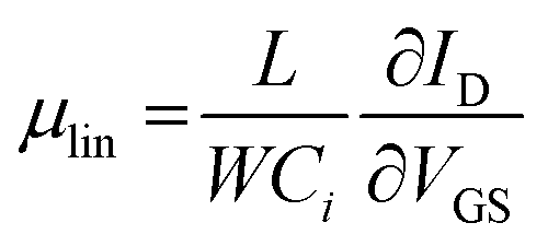 and saturation mobility to
 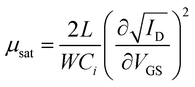 , each derived from the linear and saturation FET equation. For the calculation a capacitance of 15 nF cm−2 was used.
Results and discussion
Synthesis of CuS nanoplatelets
CuS NPLs were produced following a modified hot-injection procedure by Wu et al.67 and used as a template for a subsequent chemical transformation into PbS NPLs, as schematized in Fig. 1. XRD analysis revealed that CuS NPLs possess a covellite crystal structure with pronounced reflexes of the {006} plane resulting from their preferential orientation on a wafer (Fig. 2a). TEM images of the product showed NPLs with hexagonal shape with lateral dimensions of 40 ± 2 nm and a thickness of about 5 nm corresponding to three unit cells with regard to a lattice constant along the c axis of 1.63 nm (Fig. 2b and c).68 With the aim of increasing the lateral dimensions of the NPLs, we modified the synthetic procedure and found a size-dependence of the resulting nanodisks and -sheets on the concentration of the copper precursor (CuI), the reaction time, and the reaction temperature. When the synthesis was carried out as following the original recipe, disk-shaped CuS NPLs with a diameter of 40 ± 2 nm and a thickness of about 5 nm were formed already within 30 min after the injection of the S-precursor. The NPLs retained their morphology up to 8 h of the reaction time. However, extending the reaction time to 16 h resulted in a mixture consisting of rounded/triangular platelets and larger nanosheets with hexagonal shape with lateral sizes of up to 500 nm (Fig. 2d). Increasing the reaction temperature to 140 °C yielded disks and larger hexagons already after 30 min. After 8 h of the reaction, we obtained CuS in the form of 18–40 nm nanodisks and 85–155 nm hexagons with a small fraction of larger 900 nm nanosheets (Fig. 2e).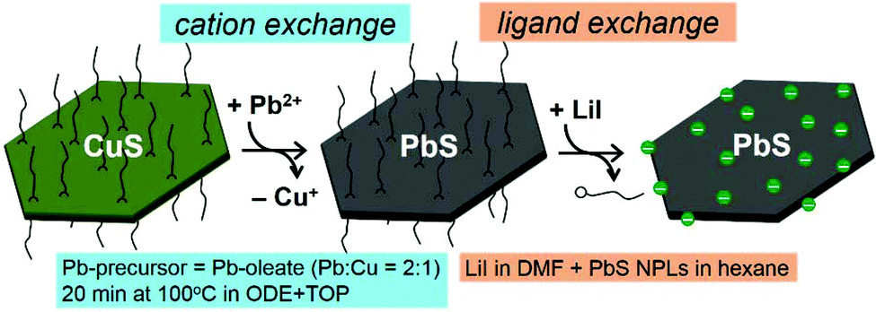 | ||
| Fig. 1 A scheme of the chemical transformations of the NPLs starting from parental CuS NPLs undergoing Cu+-to-Pb2+ cation exchange resulting in PbS NPLs, which then were subjected to ligand exchange in order to replace the insulating organic ligands with smaller I− inorganic ions. | ||
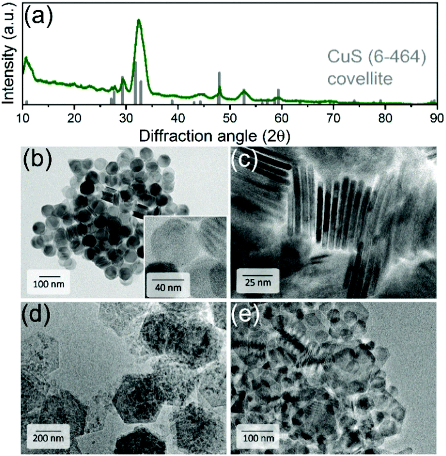 | ||
| Fig. 2 (a) XRD pattern of CuS NPLs matching to hexagonal covellite CuS structure (C6-464). TEM images show (a) an overview of CuS NPLs after 6 h of the synthesis at 120 °C with enlarged view in the inset in (b) and their thickness (c), larger CuS NPLs obtained after 16 h at 120 °C (d) and after 8 h at 140 °C (e). | ||
Furthermore, by decreasing the amount of the copper precursor, CuI, to 0.25 mmol (i.e. the Cu![[thin space (1/6-em)]](https://www.rsc.org/images/entities/char_2009.gif) :S ratio from 1:2.5 to 1:8) we did not observe a significant difference in comparison to the original procedure within the first 6 h after the injection of the S-precursor. However, after 8 hours the resulting mixture consisted of 2D NCs with a broad size distribution: rounded 20–50 nm nanodisks, triangles with a lateral size of up to 250 nm as well as hexagons with lateral dimensions from 75 to 1100 nm (Fig. SI1a and b in the ESI†). Moreover, we obtained a mixture of CuS nanodisks and hexagons with lateral sizes of up to 500 nm after 6 h by further decreasing the Cu:S ratio to 1:16 (0.12 mmol of CuI), respectively (Fig. SI1c and d†). Generally, we found that the growth of larger nanosheets was associated with increased size dispersion, suggesting that larger nanostructures grew at the expense of smaller ones via Ostwald ripening. The least polydispersity was achieved by increasing the reaction time to 16 h. The growth of larger nanosheets was also detectable using optical absorption measurements showing a much broader localized surface plasmon resonance (LSPR) in the NIR in comparison to 40 nm CuS nanodisks with a narrower absorption band (see Fig. 3b).
:S ratio from 1:2.5 to 1:8) we did not observe a significant difference in comparison to the original procedure within the first 6 h after the injection of the S-precursor. However, after 8 hours the resulting mixture consisted of 2D NCs with a broad size distribution: rounded 20–50 nm nanodisks, triangles with a lateral size of up to 250 nm as well as hexagons with lateral dimensions from 75 to 1100 nm (Fig. SI1a and b in the ESI†). Moreover, we obtained a mixture of CuS nanodisks and hexagons with lateral sizes of up to 500 nm after 6 h by further decreasing the Cu:S ratio to 1:16 (0.12 mmol of CuI), respectively (Fig. SI1c and d†). Generally, we found that the growth of larger nanosheets was associated with increased size dispersion, suggesting that larger nanostructures grew at the expense of smaller ones via Ostwald ripening. The least polydispersity was achieved by increasing the reaction time to 16 h. The growth of larger nanosheets was also detectable using optical absorption measurements showing a much broader localized surface plasmon resonance (LSPR) in the NIR in comparison to 40 nm CuS nanodisks with a narrower absorption band (see Fig. 3b).
 | ||
| Fig. 3 (a) XRD pattern of PbS NPLs matching the PbS galena crystal phase (C5-592). (b) Absorption spectra of CuS NPLs obtained after 6 h or 16 h at 120 °C and PbS NPLs after the exchange. TEM (c) and HRTEM (d) images of PbS NPLs. | ||
Cation exchange Cu+-to-Pb2+ in CuS nanoplatelets
To transform CuS into PbS, a modified procedure based on previously described methods was utilized, in which the CE reaction was completed within 20 min.44,59,61,69 The key aspects for the successful CE reaction from CuS to PbS maintaining the original shape and size are (1) moderate excess of Pb-precursor relative to copper (Pb:Cu ratio = 2:1); (2) moderate reaction temperature (100 °C); (3) the use of TOP that favors the extraction of Cu+ from the NPLs, since TOP as a soft base binds stronger to the softer acid Cu+, than to harder Pb2+, by donating its lone electron pair forming a Cu–P(C8H17)3 complex;70 and (4) the additional role of TOP as a reducing agent, which enables breaking the covalent S–S bonds within the CuS covellite structure.
After CE, the NPLs were characterized by means of XRD analysis, absorption spectroscopy and TEM imaging. XRD revealed the cubic galena structure of PbS NPLs with more pronounced reflexes of the {111} facet (Fig. 3a). In absorption spectra, the strong LSPR of the parental CuS NPLs vanished and we observed a broad absorption characteristic related to PbS nanostructures with a pronounced shoulder at approx. 1500 nm (Fig. 3b). In fact, the plasmon band disappeared already after 2 min of the reaction that in combination with XRD results, showing a pure galena pattern, suggest fast CE (Fig. SI2†). We used a longer reaction time in order to decrease the content of residual copper atoms in the structure. ICP-OES analysis determined the Pb:Cu ratio being 1:0.08, indicating a remarkable residue of remaining copper atoms in the structure. Fig. 3c and d displays TEM images of the product, which mainly consisted of small hexagonal NPLs and larger nanosheets preserving their shape and lateral dimensions. The thickness is assumed to be maintained as well, although its direct measurements during the TEM imaging was impossible since all nanostructures laid flat on the grids and did not form stacks most probably due to their rough (not atomically flat) surface. Unlike the parent monocrystalline CuS NPLs, PbS NPLs were built of smaller crystallites, as follows from the HRTEM imaging (Fig. 3d). Summarized, our approach provides an efficient chemical conversion from CuS covellite (hexagonal) to PbS galena (cubic) NPLs, while preserving their anisotropic 2D shape and the size. The examination of the exchange mechanism giving a detailed insight into the structural changes is part of our future research. Here we would like to point attention of the reader to several recent works reporting detailed studies of partial CE Cu+-to-Cd2+, -Hg2+,71,72 -Au3+,73,74 -Ag+,74 -Zn2+, -Pb2+, -In3+, -Fe3+, -Ga3+, -Sn4+, and -Ge4+ (ref. 72) on covellite CuS NCs, which provide valuable insights into the mechanism of the exchange.
Ligand exchange
Based on previously reported methods, we examined different halides to replace the long-chain OlAc residues from the surface of PbS NPLs in order to enhance interparticle coupling as well as to improve the colloidal stability, since the as-synthesized PbS NPLs agglomerated rapidly being dispersed in non-polar organic solvents, such as toluene or hexane. In LE reactions we used biphasic solvent systems: either hexane/DMF, hexane/MFA, or toluene/FA. As precursors for the LE we tested NH4I, PbI2, LiBr, and LiI. With the exception of FA as a solvent, we found a complete transfer of PbS NPLs from the non-polar phase into the polar solvent indicating a successful ligand replacement for all systems. After washing, PbS NPLs could also be well dispersed in a corresponding polar solvent used in the exchange. However, upon employing NH4I solutions in FA, MFA, and DMF (concentrations varied from 0.1 to 1 M), TEM imaging revealed broken NPLs and nanostructures of undefined shape (Fig. SI3a and b†). In the case of MFA, the initial morphology was no longer recognizable (Fig. SI3a†). In addition, when working with NH4I, the CuS NPL dispersion turned slightly blue. The broken NPL structure may result from the complexation of Cu residues, which is consistent with our observations, as copper forms blue colored, stable complexes with ammonia. Nevertheless, we successfully stabilized PbS NPLs using 1 M LiI or 0.25 M PbI2 solutions in DMF (Fig. SI3c and d†). A prompt processing as soon as the LE is completed, keeping washings steps at a low number, and storage in DFP instead of DMF are crucial for the preservation of the NPL morphology, as can be seen in Fig. SI4.† According to this optimized procedure, which we used in all further experiments, as soon as all NPLs were transferred to the bottom phase with lithium or lead iodide, the hexane phase was discarded and the PbS NPLs were collected by centrifugation and once more redispersed in DMF in order to remove excess amount of ligands. The NPLs were again centrifuged and finally redispersed in DFP. TEM characterization of the phase transferred material in DFP showed the integrity of the hexagonal NPLs and larger nanosheets (Fig. SI3c and d†), whereas XRD analysis confirmed the preservation of PbS galena crystal structure (not shown). The overall integrity of the resulting PbS NPLs is apparent by comparing TEM images of CuS and PbS NPLs before and after LE acquired at different magnifications (Fig. SI5†). Both the larger hexagons and the smaller disks retained their size and shape and the samples show a comparable composition after all procedures. The pronounced agglomeration of the organic-capped CuS and PbS NPLs is notable in the images. In attempt to separate the NPLs of different sizes, we applied size selective precipitation via gradient centrifugation (5000 rpm, 15 s). Even though it was possible to reduce the quantity of small nanodisks in a sample by precipitating large NPLs, we could not achieve a complete separation due to a partial aggregation of small and large species, i.e. smaller disks tended to deposit onto the surface of larger NPLs (Fig. SI6†).
Fig. 4a compares absorption spectra of PbS NPLs with organic ligands dispersed in TCE with those capped with LiI deposited on a glass substrate in the form of thin films. The absorption spectra of the NPLs remained almost unchanged after LE, further confirming the preservation of their integrity. ICP-OES after ligand exchange determined less Cu leading to a Pb:Cu ratio of 1:0.04 (Table SI1†). We assume that the lower copper content can be attributed to the removal of copper species on the NPL surface during LE. Furthermore, the use of PbI2 slightly increased the Pb:S ratio indicating that the typical etching of Pb2+ ions from the surface is prevented and that the surrounding of the PbS NPL consisted of I− and Pb2+ and [PbI3]− ions.75 The latter is in good agreement with the detected amount of 8% Li after LE, where the Li+ cations are the positive counter ions to the I− anions on the PbS NPL surface. EDX analysis of the copper content in individual NPLs of different sizes and shapes as well as NPL ensembles, results of which are presented in Fig. SI7,† revealed a random distribution of copper atoms all over the particles with a certain deviation, as one would expect. Overall, the stabilization by LiI proved to be more efficient in comparison to PbI2. With the latter, the PbS NPLs sedimented within 24 h, while PbS platelets capped with LiI were stable for months and only a little etching was observable after 75 days (Fig. 4b–e). The complete removal of OlAc was further substantiated by means of FTIR and XPS spectroscopies. Thus, in the FTIR spectra of the dried LiI-capped PbS NPLs no presence of organic species was detected, and especially the characteristic C–H stretching modes (2700–3000 cm−1) from OlAc completely disappeared after the LE (Fig. 4b).
 | ||
| Fig. 4 (a) Absorption and FTIR (b) spectra of PbS NPLs before and after the LE with LiI with corresponding photographs as the inset in (a). Inset in (b) shows a photograph of samples of PbS NPLs capped with either OlAc, LiI (concentrated ink and diluted dispersion), or PbI2 and dispersed in toluene or DFP after storage for one or 30 days. TEM images of PbS NPLs after LE stored in DFP over 1 day (c), 20 (d) and 75 (e) days. | ||
A more detailed picture of the LE was provided by the XPS analysis (Fig. 5). One can detect lead, sulfur, and iodide as expected, while the data for carbon and oxygen are not presented here. Fig. 5a–d shows the individual core level regions of Pb 4f, S 2p, I 3d, and Li 1s. The Pb:S ratio is calculated to be 1.36:1.0 and 1.43:1.0 before and after the LE, respectively. This ratio was calculated by taking the sensitivity factors of 10.05, 12.83, 0.567, and 1.11 (ref. 76) for Pb 4f5/2, Pb 4f7/2, S 2p1/2, and S 2p3/2, respectively; using the ratio of the Pb 4f to S 2p peak area. In the 4f5/2 and 4f7/2 spin–orbit coupled doublet of Pb, the spectra can be fitted by three Pb species before and two Pb species after the LE (see Fig. 5a). The main strong signals at 142.7 eV and 137.8 eV for Pb 4f5/2 and Pb 4f7/2, respectively, are attributed to Pb2+ ions in the bulk of the NPLs.77–79 The two weaker components at higher binding energies are assigned to the surface Pb2+ ions bound to OlAc/oleate (143.7 eV and 138.8 eV for Pb 4f5/2 and Pb 4f7/2) and to the surface Pb2+ ions bound to the amino group of the OlAm residues (144.6 eV and 139.7 eV for Pb 4f5/2 and Pb 4f7/2, respectively).77,79 After the LE, the contributions from the previous two surface components disappeared and a new component at a new biding energy (143.1 eV and 138.2 eV for Pb 4f5/2 and Pb 4f7/2, respectively) was present, which we assign to the surface Pb2+ ions bound to iodide.80 In accordance, after the LE an iodide signal appeared in the I 3d and I 4d spectral regions, as can be seen in Fig. 5c and d. The new emerging iodide features suggest that the iodide ions successfully replaced the pristine organic ligands. The lack of any Li 1s signal, expected around 54–55 eV could be explained by its low content. Supposedly, most Li+ cations left the film, probably bound to oleate, during the LE. In the case of the S 2p signal, an analysis of the XPS spectra indicates that the doublet cannot be satisfactorily fitted by a single sulfur species before LE and at least two types of sulfur are present in the NPLs (see Fig. 5b). The main signals at 162.3 eV and 161.1 eV for S 2p1/2 and S 2p3/2, respectively, we attribute to S2− ions in the bulk of the NPLs bound to Pb.78,79,81 We assign the second component at 163.0 eV and 161.8 eV to the bulk S2− ions bound to the Cu atoms,82 which remained in the NPLs after the CE process consistent with the ICP-OES results. After the LE, only the main sulfur component, Pb–S, was preserved and the signal related to Cu–S completely vanished, which is in accordance with our ICP-OES results as the removal of Cu+ bound to the surface is expected during the exchange (see Fig. 5b).
 | ||
| Fig. 5 Core level XPS spectra of Pb 4f (a), S 2p (b), I 3d (c), and Li 1s (d) region of PbS NPLs before and after the LE. | ||
Electrical conductivity and FET properties of PbS NPL thin-films
To investigate the influence of the LE on the electronic properties, we fabricated thin films of PbS NPLs by spin-coating before and after the exchange with LiI or PbI2. The films were fabricated with comparable concentrations and amounts of PbS NPL dispersions. We determined the sheet resistance RS of the initial layers processed at room temperature as well as after gradual annealing at 200 °C and 350 °C for 1 h each (Fig. 6). Based on the RS = 2.72 × 10¹³ Ω sq−1 of OlAc-capped PbS NPLs, the resistance was reduced by 4 and 5 orders of magnitude after heating to 200 °C and 350 °C, respectively. Surface modification by LE led to an additional reduction of the resistance to 2.7 × 10⁵ Ω sq−1 and 2.14 × 10⁷ Ω sq−1 for LiI- and PbI2-capped PbS NPLs, respectively. This highlights the positive effect of shorter ligands with regard to the electron mobility within the PbS thin film. In a typical procedure, CE and LE were performed in a nitrogen filled glovebox. Ambient processed PbS NPLs possess a higher sheet resistance of 3.79 × 10⁶ Ω sq−1 after LE with LiI and after annealing at 350 °C. These results underline the oxygen sensitivity of PbS, but the relatively low resistance could be assigned to the above mentioned improvement of the ambient stability by halide ligands. | ||
| Fig. 6 Sheet resistance of initial PbS OlAc-capped NPLs and after the LE as well as after the heat treatment with corresponding values obtained by handling the samples in an ambient atmosphere. | ||
Thin PbS NPL-based films could be produced via spin-coating at room temperature and used as active semiconductor layer in an FET. Therefore, we fabricated and characterized a device with a structure depicted in Fig. 7a. The LiI-capped PbS NPLs showed a p-type gate effect with a current modulation of Ion/Ioff ∼60, and a threshold voltage of Vth = −3.8 V. We measured the linear and the saturation mobilities as μlin = 0.02 cm2 (V s)−1 (VSD = −1 V) and μsat = 0.012 cm2 (V s)−1 (VSD = −20 V), respectively. The corresponding measurements are summarized in Fig. 7b and c. The low p-channel Ion/Ioff ratio presumably results from the high intrinsic conductivity of PbS NPLs doped with a remarkably high amount of residual copper. Therefore, a relatively high VDS was required in order to turn the device off. Both transfer and output characteristics show a slight hysteresis with a lower back sweep current, which can be explained by traps in the PbS NPLs or traps at the semiconductor–dielectric interface. Fast trap filling but slow releasing results then in current differences for forward and backward measurement directions. Balazs et al. also reported this behavior for their FETs using PbS colloidal quantum dot superlattices.83 Despite the fact that a subthreshold swing could not be estimated for the PbS NPL-based FETs, the charge carrier mobility as well as the on/off ratio are comparable to those of Balazs et al. (μ = 0.05 cm2 V−1 s−1, on/off ratio = 106). We suggest that by a further optimization of the material preparation, e.g. by removal of copper impurities reducing the doping of PbS NPLs, as well as of the device structure, it will be possible to significantly improve its performance.
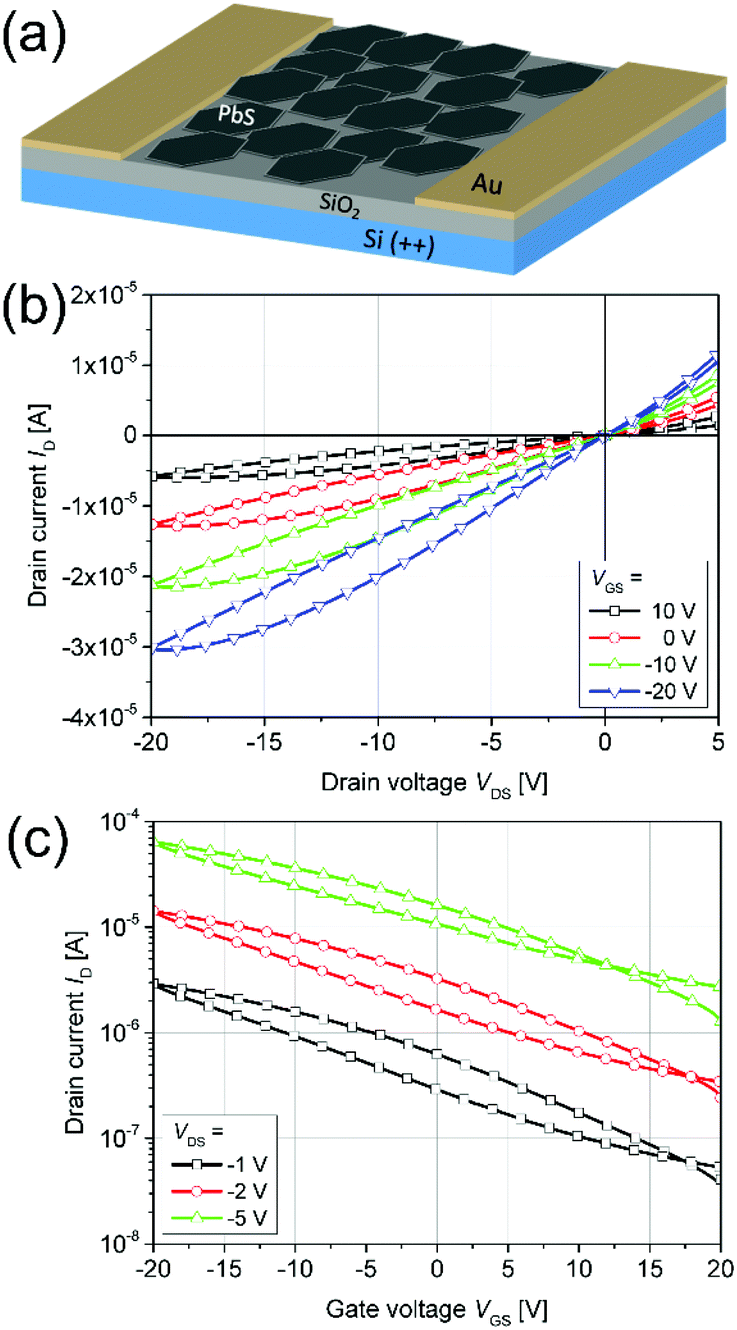 | ||
| Fig. 7 An illustration of a FET based on Li-capped PbS NPLs (a). Representative output (b) and transfer (c) characteristics. | ||
Conclusions
In this work, we synthesized CuS 2D nanostructures and increased their lateral size from 40 nm through 300 nm up to 1 μm by varying the reaction time, reaction temperature, and concentration of the copper precursor. However, an increased lateral size was accompanied by broadening of their size distribution. Afterwards, we produced PbS NPLs and larger nanosheets utilizing a cation exchange process, in which Cu+ was replaced with Pb2+ ions, while preserving the parental CuS NPL morphology. Further processing involved the ligand exchange of the initial long, insulating, organic capping molecules by inorganic iodides, which resulted in all-inorganic PbS 2D structures with an improved colloidal stability and improved electronic features. In particular, we produced colloidal dispersions of NPLs with lateral sizes of approx. 300 nm stable for a few months, which were further processed into thin films via spin-coating. The resulting films were characterized by electrical measurements, revealing benefits of the ligand exchange technique. Finally, a working FET was fabricated out of LiI-capped PbS NPLs dispersed in DFP showing a linear charge carrier mobility for holes of 0.02 cm2 V−1 s−1 with an on/off ratio of 60. These findings pave the way to a further exploitation of colloidal 2D semiconductor nanostructures in solution processed optoelectronic devices.Conflicts of interest
There are no conflicts to declare.Acknowledgements
V. L. and A. E. acknowledge the support by the DAAD projects 57447520 and 57334961. L. S. acknowledges the support by the DFG project GA 1289/3-1.References
- P. V. Kamat, J. Phys. Chem. Lett., 2013, 4, 908–918 CrossRef CAS PubMed.
- M. V. Kovalenko, L. Manna, A. Cabot, Z. Hens, D. V. Talapin, C. R. Kagan, V. I. Klimov, A. L. Rogach, P. Reiss, D. J. Milliron, P. Guyot-Sionnnest, G. Konstantatos, W. J. Parak, T. Hyeon, B. A. Korgel, C. B. Murray and W. Heiss, ACS Nano, 2015, 9, 1012–1057 CrossRef CAS PubMed.
- C. B. Murray, D. J. Norris and M. G. Bawendi, J. Am. Chem. Soc., 1993, 115, 8706–8715 CrossRef CAS.
- X. Peng, L. Manna, W. Yang, J. Wickham, E. Scher, A. Kadavanich and A. P. Alivisatos, Nature, 2000, 404, 59–61 CrossRef CAS PubMed.
- C. Bouet, B. Mahler, B. Nadal, B. Abecassis, M. D. Tessier, S. Ithurria, X. Xu and B. Dubertret, Chem. Mater., 2013, 25, 639–645 CrossRef CAS.
- T. Bielewicz, M. M. Ramin Moayed, V. Lebedeva, C. Strelow, A. Rieckmann and C. Klinke, Chem. Mater., 2015, 27, 8248–8254 CrossRef CAS.
- H. Goesmann and C. Feldmann, Angew. Chem., Int. Ed., 2010, 49, 1362–1395 CrossRef CAS PubMed.
- N. Gaponik, S. G. Hickey, D. Dorfs, A. L. Rogach and A. Eychmüller, Small, 2010, 6, 1364–1378 CrossRef CAS PubMed.
- Semiconductor Nanocrystal Quantum Dots, ed. A. L. Rogach, Springer Vienna, Vienna, 2008 Search PubMed.
- S. Dogan, T. Bielewicz, Y. Cai and C. Klinke, Appl. Phys. Lett., 2012, 101, 073102 CrossRef.
- W.-Y. Wu, S. Chakrabortty, A. Guchhait, G. Y. Z. Wong, G. K. Dalapati, M. Lin and Y. Chan, Chem. Mater., 2016, 28, 9132–9138 CrossRef CAS.
- T. Bielewicz, S. Dogan and C. Klinke, Small, 2015, 11, 826–833 CrossRef CAS PubMed.
- M. M. Ramin Moayed, T. Bielewicz, H. Noei, A. Stierle and C. Klinke, Adv. Funct. Mater., 2018, 28, 1706815 CrossRef.
- A. H. Khan, R. Brescia, A. Polovitsyn, I. Angeloni, B. Martín-García and I. Moreels, Chem. Mater., 2017, 29, 2883–2889 CrossRef CAS.
- A. D. Antu, Z. Jiang, S. M. Premathilka, Y. Tang, J. Hu, A. Roy and L. Sun, Chem. Mater., 2018, 30, 3697–3703 CrossRef CAS.
- H. Li, D. Zhitomirsky and J. C. Grossman, Chem. Mater., 2016, 28, 1888–1896 CrossRef CAS.
- G. H. Carey, A. L. Abdelhady, Z. Ning, S. M. Thon, O. M. Bakr and E. H. Sargent, Chem. Rev., 2015, 115, 12732–12763 CrossRef CAS PubMed.
- J. T. Stewart, L. A. Padilha, M. M. Qazilbash, J. M. Pietryga, A. G. Midgett, J. M. Luther, M. C. Beard, A. J. Nozik and V. I. Klimov, Nano Lett., 2012, 12, 622–628 CrossRef CAS PubMed.
- M. Aerts, T. Bielewicz, C. Klinke, F. C. Grozema, A. J. Houtepen, J. M. Schins and L. D. A. Siebbeles, Nat. Commun., 2014, 5, 3789 CrossRef PubMed.
- Y. Zhou, H. Itoh, T. Uemura, K. Naka and Y. Chujo, Langmuir, 2002, 18, 5287–5292 CrossRef CAS.
- C. Schliehe, B. H. Juarez, M. Pelletier, S. Jander, D. Greshnykh, M. Nagel, A. Meyer, S. Foerster, A. Kornowski, C. Klinke and H. Weller, Science, 2010, 329, 550–553 CrossRef CAS PubMed.
- G. B. Bhandari, K. Subedi, Y. He, Z. Jiang, M. Leopold, N. Reilly, H. P. Lu, A. T. Zayak and L. Sun, Chem. Mater., 2014, 26, 5433–5436 CrossRef CAS.
- H. Zhang, B. H. Savitzky, J. Yang, J. T. Newman, K. A. Perez, B.-R. Hyun, L. F. Kourkoutis, T. Hanrath and F. W. Wise, Chem. Mater., 2016, 28, 127–134 CrossRef CAS.
- S. M. Premathilaka, Z. Jiang, A. Antu, J. Leffler, J. Hu, A. Roy and L. Sun, Phys. Status Solidi RRL, 2016, 10, 838–842 CrossRef CAS.
- S. Acharya, B. Das, U. Thupakula, K. Ariga, D. D. Sarma, J. Israelachvili and Y. Golan, Nano Lett., 2013, 13, 409–415 CrossRef CAS PubMed.
- M. P. Boneschanscher, W. H. Evers, J. J. Geuchies, T. Altantzis, B. Goris, F. T. Rabouw, S. A. P. van Rossum, H. S. J. van der Zant, L. D. A. Siebbeles, G. Van Tendeloo, I. Swart, J. Hilhorst, A. V. Petukhov, S. Bals and D. Vanmaekelbergh, Science, 2014, 344, 1377–1380 CrossRef CAS PubMed.
- A. Mews, A. Eychmüller, M. Giersig, D. Schooss and H. Weller, J. Phys. Chem., 1994, 98, 934–941 CrossRef CAS.
- H. S. Zhou, H. Sasahara, I. Honma, H. Komiyama and J. W. Haus, Chem. Mater., 1994, 6, 1534–1541 CrossRef CAS.
- J. B. Rivest and P. K. Jain, Chem. Soc. Rev., 2013, 89–96 RSC.
- S. Gupta, S. V. Kershaw and A. L. Rogach, Adv. Mater., 2013, 25, 6923–6944 CrossRef CAS PubMed.
- B. J. Beberwyck, Y. Surendranath and A. P. Alivisatos, J. Phys. Chem. C, 2013, 117, 19759–19770 CrossRef CAS.
- L. De Trizio and L. Manna, Chem. Rev., 2016, 116, 10852–10887 CrossRef CAS PubMed.
- G. D. Moon, S. Ko, Y. Min, J. Zeng, Y. Xia and U. Jeong, Nano Today, 2011, 6, 186–203 CrossRef CAS.
- D. H. Son, S. M. Hughes, Y. Yin and A. P. Alivisatos, Science, 2004, 306, 1009–1012 CrossRef CAS PubMed.
- S. G. Kwon and T. Hyeon, Small, 2011, 7, 2685–2702 CrossRef CAS PubMed.
- V. Lesnyak, N. Gaponik and A. Eychmüller, Chem. Soc. Rev., 2013, 42, 2905–2929 RSC.
- W. Du, X. Qian, X. Ma, Q. Gong, H. Cao and J. Yin, Chem. – Eur. J., 2007, 13, 3241–3247 CrossRef CAS PubMed.
- Y. Du, Z. Yin, J. Zhu, X. Huang, X.-J. Wu, Z. Zeng, Q. Yan and H. Zhang, Nat. Commun., 2012, 3, 1177 CrossRef PubMed.
- Y. Xie, L. Carbone, C. Nobile, V. Grillo, S. D'Agostino, F. Della Sala, C. Giannini, D. Altamura, C. Oelsner, X. C. Kryschi and P. D. Cozzoli, ACS Nano, 2013, 7, 7352–7369 CrossRef CAS PubMed.
- M. Saranya, C. Santhosh, R. Ramachandran and A. Nirmala Grace, J. Nanotechnol., 2014, 2014, 321571 Search PubMed.
- X. Liu, X. Wang, B. Zhou, W.-C. Law, A. N. Cartwright and M. T. Swihart, Adv. Funct. Mater., 2013, 23, 1256–1264 CrossRef CAS.
- J. M. Luther, H. Zheng, B. Sadtler and A. P. Alivisatos, J. Am. Chem. Soc., 2009, 131, 16851–16857 CrossRef CAS PubMed.
- P. K. Jain, L. Amirav, S. Aloni and A. P. Alivisatos, J. Am. Chem. Soc., 2010, 132, 9997–9999 CrossRef CAS PubMed.
- H. Li, M. Zanella, A. Genovese, M. Povia, A. Falqui, C. Giannini and L. Manna, Nano Lett., 2011, 11, 4964–4970 CrossRef CAS PubMed.
- H. Li, R. Brescia, R. Krahne, G. Bertoni, M. J. P. Alcocer, C. D'Andrea, F. Scotognella, F. Tassone, M. Zanella, M. De Giorgi and L. Manna, ACS Nano, 2012, 6, 1637–1647 CrossRef CAS PubMed.
- B. Sadtler, D. O. Demchenko, H. Zheng, S. M. Hughes, M. G. Merkle, U. Dahmen, L.-W. Wang and A. P. Alivisatos, J. Am. Chem. Soc., 2009, 131, 5285–5293 CrossRef CAS PubMed.
- V. Lesnyak, R. Brescia, G. C. Messina and L. Manna, J. Am. Chem. Soc., 2015, 137, 9315–9323 CrossRef CAS PubMed.
- G. Gariano, V. Lesnyak, R. Brescia, G. Bertoni, Z. Dang, R. Gaspari, L. De Trizio and L. Manna, J. Am. Chem. Soc., 2017, 139, 9583–9590 CrossRef CAS PubMed.
- L. De Trizio, H. Li, A. Casu, A. Genovese, A. Sathya, G. C. Messina and L. Manna, J. Am. Chem. Soc., 2014, 136, 16277–16284 CrossRef CAS PubMed.
- S. Acharya and N. Pradhan, J. Phys. Chem. C, 2011, 115, 19513–19519 CrossRef CAS.
- Q. A. Akkerman, A. Genovese, C. George, M. Prato, I. Moreels, A. Casu, S. Marras, A. Curcio, A. Scarpellini, T. Pellegrino, L. Manna and V. Lesnyak, ACS Nano, 2015, 9, 521–531 CrossRef CAS PubMed.
- W. van der Stam, A. C. Berends, F. T. Rabouw, T. Willhammar, X. Ke, J. D. Meeldijk, S. Bals and C. de Mello Donega, Chem. Mater., 2015, 27, 621–628 CrossRef CAS.
- J. F. L. Lox, Z. Dang, V. M. Dzhagan, D. Spittel, B. Martín-García, I. Moreels, D. R. T. Zahn and V. Lesnyak, Chem. Mater., 2018, 30, 2607–2617 CrossRef CAS.
- V. Lesnyak, C. George, A. Genovese, M. Prato, A. Casu, S. Ayyappan, A. Scarpellini and L. Manna, ACS Nano, 2014, 8, 8407–8418 CrossRef CAS PubMed.
- L. De Trizio, M. Prato, A. Genovese, A. Casu, M. Povia, R. Simonutti, M. J. P. Alcocer, C. D'Andrea, F. Tassone and L. Manna, Chem. Mater., 2012, 24, 2400–2406 CrossRef CAS.
- R. G. Pearson, Inorg. Chem., 1988, 27, 734–740 CrossRef CAS.
- E. Dilena, D. Dorfs, C. George, K. Miszta, M. Povia, A. Genovese, A. Casu, M. Prato and L. Manna, J. Mater. Chem., 2012, 22, 13023 RSC.
- L. De Trizio, R. Gaspari, G. Bertoni, I. Kriegel, L. Moretti, F. Scotognella, L. Maserati, Y. Zhang, G. C. Messina, M. Prato, S. Marras, A. Cavalli and L. Manna, Chem. Mater., 2015, 27, 1120–1128 CrossRef CAS PubMed.
- D.-H. Ha, A. H. Caldwell, M. J. Ward, S. Honrao, K. Mathew, R. Hovden, M. K. A. Koker, D. A. Muller, R. G. Hennig and R. D. Robinson, Nano Lett., 2014, 14, 7090–7099 CrossRef CAS PubMed.
- L. Mu, F. Wang, B. Sadtler, R. A. Loomis and W. E. Buhro, ACS Nano, 2015, 9, 7419–7428 CrossRef CAS PubMed.
- H. Li, R. Brescia, M. Povia, M. Prato, G. Bertoni, L. Manna and I. Moreels, J. Am. Chem. Soc., 2013, 135, 12270–12278 CrossRef CAS PubMed.
- Y. Justo, B. Goris, J. S. Kamal, P. Geiregat, S. Bals and Z. Hens, J. Am. Chem. Soc., 2012, 134, 5484–5487 CrossRef CAS PubMed.
- V. Sayevich, N. Gaponik, M. Plötner, M. Kruszynska, T. Gemming, V. M. Dzhagan, S. Akhavan, D. R. T. Zahn, H. V. Demir and A. Eychmüller, Chem. Mater., 2015, 27, 4328–4337 CrossRef CAS.
- V. Sayevich, C. Guhrenz, M. Sin, V. M. Dzhagan, A. Weiz, D. Kasemann, E. Brunner, M. Ruck, D. R. T. Zahn, K. Leo, N. Gaponik and A. Eychmüller, Adv. Funct. Mater., 2016, 26, 2163–2175 CrossRef CAS.
- V. Sayevich, C. Guhrenz, V. M. Dzhagan, M. Sin, M. Werheid, B. Cai, L. Borchardt, J. Widmer, D. R. T. Zahn, E. Brunner, V. Lesnyak, N. Gaponik and A. Eychmüller, ACS Nano, 2017, 11, 1559–1571 CrossRef CAS PubMed.
- Q. Lin, H. J. Yun, W. Liu, H. J. Song, N. S. Makarov, O. Isaienko, T. Nakotte, G. Chen, H. Luo, V. I. Klimov and J. M. Pietryga, J. Am. Chem. Soc., 2017, 139, 6644–6653 CrossRef CAS PubMed.
- X. J. Wu, X. Huang, X. Qi, H. Li, B. Li and H. Zhang, Angew. Chem., Int. Ed., 2014, 53, 8929–8933 CrossRef CAS PubMed.
- M. C. Anthony, J. W. Bideaux, R. A. Bladh and K. W. Nichols, Handbook of Mineralogy: Volume I; Elements, Sulfides, Sulfosalts, Mineral Data Publishing, Tucson, AZ, 1990, p. 112 Search PubMed.
- H. McDaniel, N. Fuke, N. S. Makarov, J. M. Pietryga and V. I. Klimov, Nat. Commun., 2013, 4, 2887 CrossRef PubMed.
- J. Gui, M. Ji, J. Liu, M. Xu, J. Zhang and H. Zhu, Angew. Chem., Int. Ed., 2015, 54, 3683–3687 CrossRef CAS PubMed.
- Y. Xie, G. Bertoni, A. Riedinger, A. Sathya, M. Prato, S. Marras, R. Tu, T. Pellegrino and L. Manna, Chem. Mater., 2015, 27, 7531–7537 CrossRef CAS PubMed.
- Y. Liu, D. Yin and M. T. Swihart, Chem. Mater., 2018, 30, 1399–1407 CrossRef CAS.
- C. Hu, W. Chen, Y. Xie, S. K. Verma, P. Destro, G. Zhan, X. Chen, X. Zhao, P. J. Schuck, I. Kriegel and L. Manna, Nanoscale, 2018, 10, 2781–2789 RSC.
- A. Wolf, T. Kodanek and D. Dorfs, Nanoscale, 2015, 7, 19519–19527 RSC.
- H. Lu, J. Joy, R. L. Gaspar, S. E. Bradforth and R. L. Brutchey, Chem. Mater., 2016, 28, 1897–1906 CrossRef CAS.
- J. H. Scofield, J. Electron Spectrosc. Relat. Phenom., 1976, 8, 129–137 CrossRef CAS.
- A. André, C. Theurer, J. Lauth, S. Maiti, M. Hodas, M. Samadi Khoshkhoo, S. Kinge, A. J. Meixner, F. Schreiber, L. D. A. Siebbeles, K. Braun and M. Scheele, Chem. Commun., 2017, 53, 1700–1703 RSC.
- K. Laajalehto, I. Kartio and P. Nowak, Appl. Surf. Sci., 1994, 81, 11–15 CrossRef CAS.
- D. J. H. Cant, K. L. Syres, P. J. B. Lunt, H. Radtke, J. Treacy, P. J. Thomas, E. A. Lewis, S. J. Haigh, P. O'Brien, K. Schulte, F. Bondino, E. Magnano and W. R. Flavell, Langmuir, 2015, 31, 1445–1453 CrossRef CAS PubMed.
- L. R. Pederson, J. Electron Spectrosc. Relat. Phenom., 1982, 28, 203–209 CrossRef CAS.
- A. André, D. Zherebetskyy, D. Hanifi, B. He, M. Samadi Khoshkhoo, M. Jankowski, T. Chassé, L.-W. Wang, F. Schreiber, A. Salleo, Y. Liu and M. Scheele, Chem. Mater., 2015, 27, 8105–8115 CrossRef.
- M. C. Biesinger, B. R. Hart, R. Polack, B. A. Kobe and R. S. C. Smart, Miner. Eng., 2007, 20, 152–162 CrossRef CAS.
- D. M. Balazs, D. N. Dirin, H. H. Fang, L. Protesescu, G. H. Ten Brink, B. J. Kooi, M. V. Kovalenko and M. A. Loi, ACS Nano, 2015, 9, 11951–11959 CrossRef CAS PubMed.
Footnote |
| † Electronic supplementary information (ESI) available: Additional TEM images of cation and ligand exchanged NPLs, the results of ICP-OES and EDX analyses, additional absorption spectra and XRD pattern of intermediate samples taken during CE. See DOI: 10.1039/c9nr02437a |
| This journal is © The Royal Society of Chemistry 2019 |