
 Open Access Article
 This Open Access Article is licensed under a Creative Commons Attribution-Non Commercial 3.0 Unported Licence
Wafer-scale fabrication of high-quality tunable gold nanogap arrays for surface-enhanced Raman scattering†
Hai
Le-The‡
 *a,
Jasper J. A.
Lozeman‡
a,
Marta
Lafuente
b,
Pablo
Muñoz
c,
Johan G.
Bomer
a,
Hien
Duy-Tong
d,
Erwin
Berenschot
e,
Albert
van den Berg
a,
Niels R.
Tas
e,
Mathieu
Odijk
a and
Jan C. T.
Eijkel
a
*a,
Jasper J. A.
Lozeman‡
a,
Marta
Lafuente
b,
Pablo
Muñoz
c,
Johan G.
Bomer
a,
Hien
Duy-Tong
d,
Erwin
Berenschot
e,
Albert
van den Berg
a,
Niels R.
Tas
e,
Mathieu
Odijk
a and
Jan C. T.
Eijkel
a
aBIOS Lab-on-a-Chip Group, MESA+ Institute, Max Planck Center for Complex Fluid Dynamics, University of Twente, 7522 NB Enschede, The Netherlands. E-mail: h.lethe@utwente.nl
bNanoscience Institute of Aragon, Department of Chemical & Environmental Engineering, University of Zaragoza, 50018 Zaragoza, Spain
cOptical Sciences Group, MESA+ Institute, University of Twente, 7522 NB Enschede, The Netherlands
dFaculty of Engineering, Vietnamese German University, Thu Dau Mot City, Binh Duong Province, Vietnam
eMesoscale Chemical Systems Group, MESA+ Institute, University of Twente, 7522 NB Enschede, The Netherlands
First published on 10th June 2019
Abstract
We report a robust and high-yield fabrication method for wafer-scale patterning of high-quality arrays of dense gold nanogaps, combining displacement Talbot lithography based shrink-etching with dry etching, wet etching, and thin film deposition techniques. By using the self-sharpening of <111>-oriented silicon crystal planes during the wet etching process, silicon structures with extremely smooth nanogaps are obtained. Subsequent conformal deposition of a silicon nitride layer and a gold layer results in dense arrays of narrow gold nanogaps. Using this method, we successfully fabricate high-quality Au nanogaps down to 10 nm over full wafer areas. Moreover, the gap spacing can be tuned by changing the thickness of deposited Au layers. Since the roughness of the template is minimized by the crystallographic etching of silicon, the roughness of the gold nanogaps depends almost exclusively on the roughness of the sputtered gold layers. Additionally, our fabricated Au nanogaps show a significant enhancement of surface-enhanced Raman scattering (SERS) signals of benzenethiol molecules chemisorbed on the structure surface, at an average enhancement factor up to 1.5 × 10⁶.
Introduction
Nanometer-sized metallic nanogaps made of gold (Au) or silver (Ag) have found many applications including biomedical and chemical sensing,1 surface-enhanced Raman spectroscopy,2–7 and nonlinear optics8 due to their remarkable electrochemical and optical properties. For the surface-enhanced Raman spectroscopy, the intensity of the Raman scattering signal is boosted due to the modified emission of the scattering signal and the improved excitation of the studied molecules caused by the near-fields generated in metallic nanogap regions.9 To significantly enhance signals, the gap spacing needs to be much smaller than the incident wavelength.10 As a result, a strongly confined electromagnetic field is generated in the nanogap region by localized plasmons.11 Using metallic nanogap structures, local enhancement factors up to 109 have been achieved, thus enabling the detection of a single molecule.2,3 Many methods have been reported to fabricate metallic nanogap structures, such as electron beam lithography (EBL),5 EBL-based angular deposition,4 electrochemical deposition,12 electromigration,13 break junction,14,15 and atomic layer deposition (ALD).2,7 EBL-based methods offer a high feasibility in designing the size, position, shape and orientation of the metal nanogaps. However, their feature of serial patterning limits their use for high-yield and low-cost fabrication of large-area metal nanogap arrays. Moreover, the quality of the metal nanogaps strongly depends on the sidewall roughness of the patterned resist structures, which is mostly limited by the properties of the resist.4,5 Other indirect methods, such as electrochemical deposition, electromigration, and break junction, can produce very narrow metal nanogaps down to 5 nm.12–15 However, using these methods it is difficult to design a reproducible fabrication process, and thus they are unsuitable for mass production at low-cost. ALD has recently come to be considered as an effective method to pattern well-defined metal nanogaps as narrow as 3 nm.2,7 However, the fabrication process involves many complicated steps, which makes it time consuming. Additionally, the metal nanogaps patterned by the ALD technique cannot be rapidly reproduced, whereas other template-based methods allow the metal nanogaps to be reused by replacing the metal layer sputtered over the template surface. Therefore, there is a need for a robust fabrication technique for wafer-scale patterning of dense metal nanogap arrays at high throughput but low-cost.Recently, a compelling technique for patterning periodic nanostructures has been reported by Solak et al., termed displacement Talbot lithography (DTL).16 Using this technique with a monochromatic UV beam (365 nm wavelength) allows high-yield patterning of highly ordered photoresist (PR) nanostructures, i.e. lines, holes or dots, with dimensions down to approximately 100 nm, over full wafer areas. However, patterning PR nanostructures smaller than 50 nm using this technique still requires the use of a deep-UV laser, i.e. an ArF laser at 193 nm wavelength. To overcome this limitation, we developed a robust technique for shrink-etching the patterned PR nanostructures using a mixture of O2/N2 plasma.17 As a result, bottom antireflection coating (BARC) nanostructures with dimensions down to sub-30 nm could be reliably fabricated from the initially patterned PR nanostructures.
In this paper, we report and demonstrate a robust and high-yield method for wafer-scale patterning of dense arrays of tunable Au nanogaps, combining the DTL-based shrink-etching technique with dry etching, wet etching, and thin film deposition techniques. Silicon (Si) structures consisting of extremely smooth nanogaps were fabricated by combining the dry etching process with the self-sharpening of <111>-oriented Si crystal planes during the wet etching process. Such etching combination has been reported and used to fabricate various Si-based structures.18–23 Subsequent conformal deposition of a silicon nitride layer and a gold layer resulted in dense arrays of high-quality gold nanogaps over full wafer areas. The gap spacing can be tuned down to 10 nm at high uniformity by changing the Au layer thickness. Moreover, we showed the potential of our fabricated Au nanogaps for surface-enhanced spectroscopy by measuring SERS signals of benzenethiol (BT) molecules chemisorbed on the structure surface.
Experimental section
Patterning periodic 50 nm BARC nanolines
A BARC layer of 187 ± 2 nm (AZ BARLi II 200, MicroChem Corp., Japan), and a PR layer of 200 ± 2 nm (PFI88 photoresist diluted 1![[thin space (1/6-em)]](https://www.rsc.org/images/entities/char_2009.gif) :1 with propylene glycol methyl ether acetate (PGMEA), Sumitomo Chemical Co., Ltd, Japan) were spin-coated on the surface of an oxidized (∼30 nm thick SiO2) 4-inch Si wafers (525 μm thick, P-type, <100>, single side polished, Okmetic, Finland), followed by baking at 185 °C for 1 min and 90 °C for 1 min, respectively (Fig. 1a). DTL (PhableR 100C, Eulitha, Switzerland) was utilized to pattern PR nanolines of approximately 110 nm in width (250 nm pitch) at an exposure dose of 1 mW cm−2 for 75 s, using a wafer-scale phase shift mask of 250 nm grating period purchased from Eulitha (Fig. 1b). After the exposure, the oxidized Si wafer was post-exposure baked on a hotplate at 110 °C for 1 min, developed in the OPD4262 developer for 1 min, and rinsed with DI water to complete the fabrication of PR nanoline arrays (Fig. 1c). It is worth mentioning that the patterned PR nanolines were aligned to the [110] crystal orientation of the Si wafers – PR nanolines were patterned perpendicularly to the primary flat of the Si wafers. Subsequently, these PR nanolines were shrink-etched into ∼50 nm BARC nanolines, using a two-step reactive plasma etching process, i.e. 50/50 sccm O2/N2 plasma for 1 min and 45 s, and 50 sccm N2 plasma for 2 min (Fig. 1d). These plasma etching processes were conducted using a wafer-scale parallel plate reactive ion etching system (in-house built TEtske system, NanoLab Cleanroom) at 13 mTorr, and 25 W.17
:1 with propylene glycol methyl ether acetate (PGMEA), Sumitomo Chemical Co., Ltd, Japan) were spin-coated on the surface of an oxidized (∼30 nm thick SiO2) 4-inch Si wafers (525 μm thick, P-type, <100>, single side polished, Okmetic, Finland), followed by baking at 185 °C for 1 min and 90 °C for 1 min, respectively (Fig. 1a). DTL (PhableR 100C, Eulitha, Switzerland) was utilized to pattern PR nanolines of approximately 110 nm in width (250 nm pitch) at an exposure dose of 1 mW cm−2 for 75 s, using a wafer-scale phase shift mask of 250 nm grating period purchased from Eulitha (Fig. 1b). After the exposure, the oxidized Si wafer was post-exposure baked on a hotplate at 110 °C for 1 min, developed in the OPD4262 developer for 1 min, and rinsed with DI water to complete the fabrication of PR nanoline arrays (Fig. 1c). It is worth mentioning that the patterned PR nanolines were aligned to the [110] crystal orientation of the Si wafers – PR nanolines were patterned perpendicularly to the primary flat of the Si wafers. Subsequently, these PR nanolines were shrink-etched into ∼50 nm BARC nanolines, using a two-step reactive plasma etching process, i.e. 50/50 sccm O2/N2 plasma for 1 min and 45 s, and 50 sccm N2 plasma for 2 min (Fig. 1d). These plasma etching processes were conducted using a wafer-scale parallel plate reactive ion etching system (in-house built TEtske system, NanoLab Cleanroom) at 13 mTorr, and 25 W.17
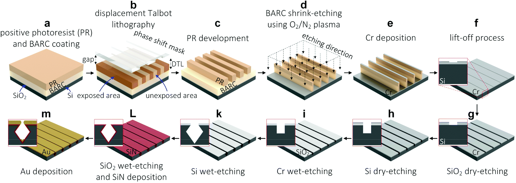 | ||
| Fig. 1 Fabrication process of high-quality tunable Au nanogap arrays. | ||
Patterning periodic Cr nanolines using lift-off process
A thin Cr layer of approximately 6 nm was deposited over the surface of the patterned wafer using a sputtering system (in-house built T'COathy system, NanoLab Cleanroom) (Fig. 1e). The sputtering process was conducted at 200 W, and a pressure of 6.6 × 10⁻³ mbar adjusted by using an argon (Ar) flow. Subsequently, a lift-off process was performed in a 99% HNO3 solution, followed by sonication in DI water for 10 min. As a result, periodic Cr nanolines of approximately 200 nm in width (250 nm pitch) were fabricated on the surface of the oxidized Si wafer (Fig. 1f). These Cr nanolines were then used as a hard mask for further processing of both the SiO2 masking layer and the bulk Si substrate.Patterning high-quality SiN nanogaps
Reactive plasma etching was used to directionally etch the SiO2 masking layer and the bulk Si substrate, which resulted in periodic Si nanotrenches of ∼50 nm in width and ∼150 nm in depth (Fig. 1g–h). This plasma etching was also conducted in the TEtske system at wafer-level, 25 sccm fluoroform (CHF3), 5 sccm O2, 10 mTorr, and 25 W for 13 min. Thereafter, the Cr mask was removed completely in a Cr etchant solution (Cr etch 200, MicroChemicals GmbH, Germany), leaving the SiO2 nanolines as a masking layer (Fig. 1i). After rinsing with DI water and drying with N2, the patterned wafer was cleaned in the O2 plasma (TePla 300, PAV TePla AG, Germany) at 500 W for 20 min. Subsequently, the fabricated Si nanotrenches were etched in a 25% KOH solution at 75 °C for 15 s (Fig. 1k), cleaned using the standard RCA-2 cleaning process, and immersed in a 50% HF solution for 10 min to completely remove the SiO2 masking layer, thus leaving only the Si structures as a template for the deposition of a low stress silicon nitride (SiN) layer.Prior to the deposition of the SiN layer, the wafer was cleaned in a 99% HNO3 solution for 10 min, in a 69% HNO3 solution at 95 °C for 10 min, in DI water using a quick dump rinser, and spin-dried. A thin SiN layer of approximately 35 nm was deposited over the Si template by using low-pressure chemical vapor deposition (LPCVD) in a high temperature tube furnace (Tempress Systems, Inc., The Netherlands) at 850 °C for 40 min (Fig. 1L). The thickness of the deposited SiN layer was measured using an ellipsometry system (M-2000UI, J.A. Woollam Co., United States) at an angle of 75°.
Patterning high-quality tunable Au nanogaps
Au layers at different thicknesses were deposited over the SiN-coated Si templates by using the T'COathy sputtering system at 200 W, 6.6 × 10⁻³ mbar.24 By adjusting the sputtering time, Au nanogaps of different gap spacings down to ∼10 nm were fabricated over full wafer areas (Fig. 1m). It is worth mentioning that all the deposited Au layers were treated with UV-ozone (PR-100 UV-ozone Photoreactor, UVP Inc., United States) for 5 min.High-resolution scanning electron microscopy (HR-SEM) images were taken by using a HR-SEM system (FEI Sirion microscope, United States) at a 5 kV acceleration voltage and a spot size of 3. The surface roughness of the deposited Au layers was determined from atomic-force microscopy (AFM) images (scan field: 500 × 500 nm2), recorded in contact modes using an AFM system (Dimension Icon, Bruker Corp., United States) in air.
Finite-difference time-domain simulations
The plasmonic behavior of the Au nanogaps was simulated by using finite-difference time-domain (FDTD) method by means of a commercial software package (Lumerical Solutions Inc., FDTD solutions). The dimensions of the Au nanogap structures were determined from the HR-SEM images. Given the translational symmetry of the structures, two-dimensional FDTD simulations were performed. Conformal mesh (mesh accuracy 4) and mesh refinement were used to define the structure with a minimum mesh size of 0.1 nm. Antisymmetric boundary conditions were used in both boundaries in the x-axis to simulate an infinitely periodic array of Au nanogaps, thus reducing the computational time. Perfectly matched layer (PML) boundary conditions with a steep angle profile were selected along the y-direction, which, ideally, absorb all incident light without creating any back reflections. A plane wave source propagating in the y-direction with an electric field parallel to the x-direction was employed to excite the surface plasmons. Convergence test was made to determine the optimum distance between the SERS structure and the PML boundary conditions in the y-axis (2 μm). The values of the dispersion relations for the different materials used (Au and Si) were extracted from the literature.25 To represent the dispersion relation of the Si3N4 material, a Cauchy model26 with coefficients of B = 1.9832, C = 0.0096, and D = 6 × 10⁻⁴ extracted from the characterization of a Si3N4 layer by ellipsometry, was used. The auto shutoff intensity was fixed at 1 × 10⁻⁶, and an excitation wavelength of 785 nm was used in the simulations.Reflection measurements
Reflection measurements were performed on different Au nanogap samples featuring different gap spacings, i.e. ∼30 nm, ∼20 nm, and ∼10 nm, in order to determine the reflection minimum of the different gap spacings. These reflection spectra were used to select the proper excitation wavelength for the FDTD simulations and the SERS measurements. The reflection measurements were conducted by using a microscope (Leica DM6000 FS microscope fitted with an Ocean Optics HR4000 detector, Germany) with a bright light source (Leica type 11307072060, Germany). A 100× magnification, and a numerical aperture of 0.9 was used for the measurements. A continuous gold substrate was used as a background for the reflection measurement.Surface-enhanced Raman scattering measurements
For the Raman measurements, a confocal Raman microscope (WITec Alpha300R, Germany) fitted with an UHTS300 spectrometer was used. The laser wavelength was chosen based on the result of the reflection measurements. Two different laser sources were used for the Raman measurements, i.e. a laser with an excitation wavelength of 785 nm (Topica Photonics XTRA 785 nm single frequency diode laser), and a laser with a wavelength of 532 nm (WITec 532 nm laser). The laser was focused on the substrate using a lens with a 100× magnification, and a numerical aperture of 0.9. The Raman microscope was operated in a backscatter configuration. The elastically backscattered excitation beam was filtered from the spectrum using an edge filter. Polarization of the light beam with respect to the sample was controlled by rotating the sample using a rotation plate for rough alignment and a half-wave dish for precise alignment. The integration time was 100 ms, and the power applied was 20 mW. It has to be noted that the measured signals were stable at this applied power. For the samples, a 5 × 5 μm2 map of 2500 measurements was created, in which for every point in the map the enhancement factor was calculated without performing the averaging. For the reference BT sample, a total of nine measurements were performed and averaged before being used to calculate the enhancement factor.In this paper, BT molecule was chosen as a reference molecule as it is generally accepted as a reference molecule to determine SERS enhancement factors in literature.27–29 Moreover, it can form a well-defined monolayer over the structure surface, and has strong Raman peaks. A monolayer of BT molecules was deposited on the Au nanowires by immersing the Au nanogaps in a 10 mM solution of BT molecules in ethanol for 15 hours. Before immersing completely in the solution, the Au nanogaps were slowly immersed perpendicularly to the solution surface so that the solution could enter all Au nanogaps by capillary flow. Subsequently, the Au nanogaps were rinsed with ethanol, and dried with N2 gas. After the functionalization of the Au nanogaps, SERS Raman spectra were measured. In addition, a neat BT solution in a glass vial was also measured using the same power and same integration time as for the SERS measurements, which was then used to determine the enhancement factor.
Determination of the enhancement factor
A large variety of methods have been reported to determine the enhancement factor of a SERS substrate.30 However, each of them has its own advantages and disadvantages, and the reported enhancement factors vary widely depending on the method used. In this paper, we used a method reported and used by Pilot et al.,29 Le Ru et al.,30 and Lin et al.31 In this method, the enhancement factor is calculated by comparing the normalized results of a SERS structure, functionalized with a reference molecule (BT), against the normalized results of the neat solution of the same reference molecule. The enhancement factor is approximated from the following equation:29 | (1) |
The normalized collection efficiency was obtained by taking several Raman spectra of a Si wafer at various positions along the z-axis. For each spectrum, the area of the Si peak at 520 cm−1 was then obtained, and then normalized against the area measured at the focal point. The result obtained was a bell-shaped curve with the offset from the focal point on the y-axis and the normalized area on the x-axis (Fig. S17†).
Results and discussion
Patterning periodic 50 nm BARC nanolines
Fig. 2a shows the HR-SEM images of periodic PR nanolines patterned on an oxidized Si wafer applying DTL. The top-view image shows well-fabricated PR nanolines (250 nm pitch) with a high uniformity in terms of the line width. The width of the PR nanolines was approximately 114 nm with a relatively small variation (standard deviation) of 2 nm. For the uniformity measurement of the fabricated PR nanolines, four areas were selected over a full wafer area (Fig. S1–S2†). The cross-sectional image shows a highly vertical PR sidewall, thus indicating a robust fabrication process achieved by applying the DTL technique.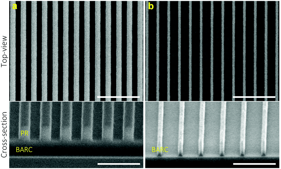 | ||
| Fig. 2 Top-view (scale bar: 1 μm) and cross-sectional (scale bar: 500 nm) HR-SEM images of (a) periodic PR nanolines, and (b) ∼50 nm BARC nanolines shrink-etched from the patterned PR nanolines. | ||
Fig. 2b shows the HR-SEM images of BARC nanolines shrink-etched using a mixture O2/N2 plasma, starting from the patterned PR nanolines. It is remarkable that the BARC nanolines were found to be still uniform over a full wafer area (Fig. S3†), and that their sidewalls remained highly vertical after the shrink-etching process, as shown in the cross-sectional image. These periodic BARC nanolines of 50 ± 3 nm in width were subsequently used as a template to pattern Cr nanolines by using a lift-off process.
Patterning periodic Cr nanolines using lift-off
Fig. 3a shows a top-view HR-SEM image of periodic Cr nanolines (∼6 nm thickness) patterned on the surface of an oxidized Si wafer. A high width uniformity of the fabricated Cr nanolines was obtained over a full wafer area (Fig. S4†), with an average width of approximately 50 nm. It is worth mentioning that the lift-off process was conducted in a 99% nitric acid (HNO3) solution as BARC cannot be dissolved in acetone. Moreover, the patterned wafer needs to be immersed immediately into DI water for sonication after the immersion in the HNO3 solution as drying the wafer before the sonication could result in the permanent sticking of unwanted Cr residues on its surface (Fig. 3b). Such Cr residues are attributed to the collapse of a Cr layer deposited on the sidewall of the BARC nanolines during the sputtering process. In addition, deposition of a thick Cr layer of approximately 12 nm also made it difficult to obtain the complete lift-off of Cr (Fig. 3c). We attribute this to the fact that the Cr layer completely covered the BARC nanolines, thus preventing the diffusion of HNO3 to completely dissolve the BARC.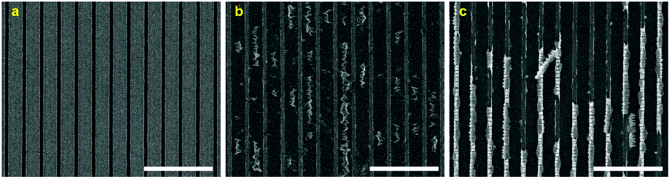 | ||
| Fig. 3 (a) Top-view HR-SEM image of periodic Cr nanolines with ∼50 nm spacing fabricated by using a lift-off process. (b) Unwanted Cr residues caused by drying the wafer before the sonication in DI water. (c) A thick deposited Cr layer (∼12 nm thick) resulted in an undesired structure after the lift-off process. Scale bar represents 1 μm. | ||
Patterning high-quality SiN nanogaps
Fig. 4a shows the HR-SEM images of Si nanotrenches after directionally dry etching the bulk Si in a parallel plate reactive ion etching system (in-house built TEtske system, NanoLab Cleanroom). From the cross-sectional image, a well-defined pattern of Si nanotrenches that have relatively vertical sidewalls is seen, indicating an anisotropic etching process. Moreover, the top-view image shows no damage to the area that is protected by the Cr layer after the etching process. This indicates that a continuous Cr layer was formed at the thickness of approximately 6 nm, and that this Cr layer was sufficient to withstand the etching of the SiO2 masking layer and the bulk Si substrate for 13 min (∼150 nm deep in Si). It is clear from the cross-sectional image that the top edge of the SiO2 masking layer was slightly damaged. We attribute this damage to the faceting formation at these SiO2 edge regions during the dry etching process. However, such damage was not found to affect the formation of Si structures after the wet etching in a potassium hydroxide (KOH) solution (Fig. 4b). A high uniformity of the etched profile into the sidewall of the Si nanotrenches was obtained, in which the etching virtually ceased at <111>-oriented Si crystal planes (etching rate of 12.5 nm min−1). It is worth noting that over-etching of the wafer in the KOH solution could lead to the formation of undesirable v-grooves in the bulk Si substrate (Fig. S5†). After wet etching of the SiO2 masking layer, a dense array of extremely smooth Si nanogaps of approximately 120 nm (250 nm pitch) was obtained (Fig. 4c). Since the roughness effects of the patterned Cr nanolines and SiO2 masking layer on the quality of the Si nanogaps are eliminated by the subsequent crystallographic etching of Si, using this Si template for further patterning of Au nanogaps significantly improves their quality.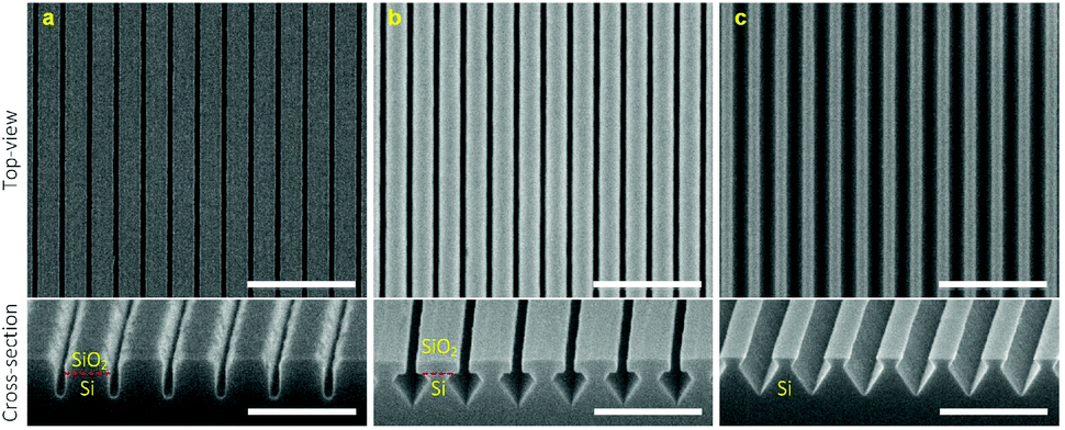 | ||
| Fig. 4 Top-view (scale bar: 1 μm) and cross-sectional (scale bar: 500 nm) HR-SEM images of the fabricated (a) Si nanotrenches after dry etching, (b) Si structure after wet etching in the KOH solution, and (c) after wet etching of the SiO2 masking layer. | ||
Fig. 5 shows the HR-SEM images of a fabricated Si template after coating with a SiN layer. The top-view image shows well-defined SiN nanolines with high uniformity in width (∼200 nm) and periodicity (∼250 nm) (Fig. S6†). It can be observed from the cross-sectional image that the SiN layer (∼35 nm thick) was conformally deposited over the Si template, resulting in very smooth and uniform SiN nanogaps of approximately 50 nm (Fig. 5b).
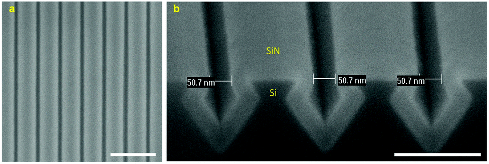 | ||
| Fig. 5 (a) Top-view (scale bar: 500 nm) and (b) cross-sectional (scale bar: 200 nm) HR-SEM images of a fabricated Si template coated with a SiN layer. | ||
Patterning high-quality tunable Au nanogaps
Fig. 6a shows the HR-SEM images of a dense array of high-quality Au nanogaps fabricated by sputtering a Au layer over the SiN-coated Si template. A high uniformity in gap spacing of the fabricated Au nanogaps was obtained over a full wafer area (Fig. S7†). It is worth noting that the top-view HR-SEM images of the Au nanogaps fabricated from different batches showed a high reproducibility of the fabrication process (Fig. S8†). It is clearly shown in the cross-sectional image that the sputtered Au layer completely covered the structure surface. It is worth mentioning that no metallic adhesion layer was used to improve the adhesion of the sputtering Au layer with the SiN surface. Therefore, the adverse effects caused by metallic adhesion layers on the optical and electrical properties of pure Au were eliminated.38,39Fig. 6b shows a close-up top-view HR-SEM image of Au nanogaps after the sputtering of a Au layer approximately 113 nm thick. Well-defined Au nanogaps of approximately 10 nm were fabricated at the periodicity of 250 nm. Since the roughness of the template was minimized by the crystallographic etching of Si, the roughness of the Au nanogaps depended almost exclusively on the roughness of the sputtered Au layers. Decreasing the thickness of the Au layer was found to decrease its roughness (Fig. S9–S11†),40 though the Au gap spacing became wider (Fig. 6c–e). This can be improved by depositing a thicker SiN layer than the currently used SiN layer of ∼35 nm, thus narrowing down the SiN nanogaps. Then, a thinner gold layer is required in order to obtain a similar Au gap spacing.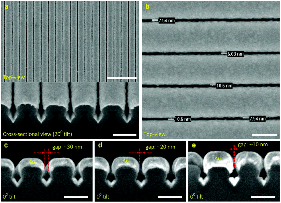 | ||
| Fig. 6 (a) Top-view (scale bar: 1 μm) and cross-sectional (scale bar: 200 nm) HR-SEM images of a fabricated array of Au nanogaps. (b) A close-up HR-SEM image (scale bar: 200 nm) shows well-defined Au nanogaps with a gap spacing of approximately 10 nm. The gap spacing was tuned from (c) ∼30 nm to (d) ∼20 nm, and (e) ∼10 nm by increasing the thickness of the deposited Au layers from ∼67 nm to ∼90 nm, and ∼113 nm, respectively. Scale bars represent 200 nm. | ||
In our fabrication process, only the photoresist nanolines are serially patterned (approximately 10 min per wafer), whereas the other processes can be performed in batch. All together, the process may offer a unique combination of high geometrical control and a good potential for low-cost production. Furthermore, it is worth mentioning that our SiN-coated Si templates can be reused by replacing the Au layer with another fresh layer, without damaging the template material or altering its dimensions.
Finite-difference time-domain simulations
Fig. 7 shows the finite-difference time-domain (FDTD) simulation results of the local field intensity enhancement factor at Au nanogaps with different gap spacings at the excitation wavelength of 785 nm. The color scale represents the normalized amplitude of the enhanced electric field |E| with respect to the amplitude of the incoming electric field |E0|. As can be seen in Fig. 7, the reduction of the gap spacing resulted in an increase in the enhanced electric field at the Au nanogap region, which can be explained from the increasing surface plasmon resonance (SPR) strength when decreasing the gap spacing.41,42 Similar results have also been reported for different structures when reducing the gap spacing.42,43 In addition, Fig. 7c clearly shows that there are two major regions of the enhanced electric field generated within the ∼10 nm Au nanogaps. Awang et al. reported a similar observation when simulating the electric field distribution within the gap of the Au nanograting pairs supported on the SF10 glass substrate,43 which they attributed to the corner effect of the structure.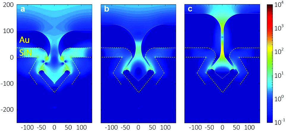 | ||
| Fig. 7 FDTD-simulated distribution of the local field intensity enhancement factor (|E|2/|E0|2) at the wavelength of 785 nm for Au nanogaps of (a) ∼30 nm, (b) ∼20 nm, and (c) ∼10 nm. The yellow dashed lines indicates the SiN boundary. | ||
Surface-enhanced Raman scattering measurements
Fig. 8a shows the reflectance spectra measured on various Au nanogap samples containing different gap spacings. A red shift and formation of a second peak at ∼525 nm were observed in the spectra when reducing the gap spacing. The appearance of such second peak at lower wavelengths has been reported in the literature, both for two nanoparticle systems44 and nanowires.5 Romero et al. attributed the formation of these peaks to the strong interactions of single particle multipoles.45 However, it has to be noted that the explanation of Romero et al. was based on the two nanosphere system.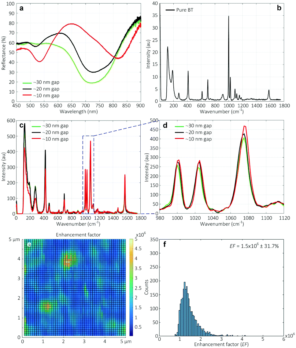 | ||
| Fig. 8 (a) Reflectance spectra. SERS signals (b) of pure BT, and (c) measured on Au nanogap arrays of ∼30 nm, ∼20 nm, and ∼10 nm gap spacing, with (d) a close-up image. (e) Calculated enhancement factors of the spectra obtained from the measurements over a 5 × 5 μm2 area for the ∼10 nm Au nanogaps, and (f) the corresponding histogram. | ||
Fig. 8b shows the SERS signal of the pure BT used as the reference. Fig. 8c shows the SERS signals measured on various Au nanogap samples containing different gap spacings of ∼30 nm, ∼20 nm, and ∼10 nm, after coating a monolayer of BT molecules. As can be seen at the 1070 cm−1 peak in Fig. 8d, there is a slight increase in the measured signal with decreasing gap spacing from ∼30 nm to ∼10 nm. It might be surprising that the enhancement in the electric field strength in the simulated gap region (see Fig. 7), which is about 10-fold from the ∼20 nm to ∼10 nm gaps, causes only a relatively small increase in the measured signal. However, this can be explained by the fact that the fraction of the scattered signal that reaches the objectives (NA = 0.9, αadm ≈64°) decreases with an increasingly narrow gap and consequently lower escape angle. It must furthermore be noted that the BT monolayer forms only on the sample surface after drying (white lines in Fig. 7), so that the high field enhancement in the entire gap in the ∼10 nm Au nanogaps does not contribute to the measured SERS signal (Fig. S12–S13†). It is thus expected that the ∼10 nm Au nanogaps are especially useful for measuring in solution.
It is worth mentioning that all the Au nanogaps were slowly immersed perpendicularly to the BT solution surface before immersing completely in the solution. We expect that the solution could wet the entire Au nanogaps by the capillary flow. This procedure was followed because immersing the Au nanogaps into the BT solution, parallel to the solution surface, resulted in a significant drop in the signal intensity, especially for the ∼10 nm Au nanogaps (Fig. S14†). We attribute this to a lack of penetration of the solution with analyte molecules to the region of the nanogaps, caused by the hydrophobic nature of Au. Therefore, in that case, although there is a strongly enhanced electric field at this region (see Fig. 7), a lower SERS signal is generated, leading to a significant drop in the totally obtained signal. This would imply that the method of sample introduction is an important factor in the present SERS structures.
To investigate the homogeneity of the enhancement over the structure surface, a map of 5 × 5 μm2 containing 2500 excitation points (50 lines containing 50 points per line) was constructed, and the enhancement factor was calculated using eqn (1). As shown in Fig. 8e, for the Au nanogaps of ∼10 nm gap spacing, a relatively high uniformity in the enhanced factor was obtained (Fig. 8f). For the structures with gap spacings of ∼30 nm and ∼20 nm, the maps of the enhancement factor are shown in Fig. S15.†
The average enhancement factors calculated by averaging 2500 spectra of each map and their relative standard deviation were 1.1 × 10⁶ ± 19.7%, 1.1 × 10⁶ ± 22.7%, and 1.5 × 10⁶ ± 31.7% for the Au nanogaps of ∼30 nm, ∼20 nm, and ∼10 nm, respectively (Fig. S16–S17†). These obtained enhancement factors are comparable to those reported in the literature35–37 at similar gap spacings. These enhancement factors are expected to be enhanced by further narrowing down the gap spacing. This can be done by conformal deposition of a thicker SiN layer than the currently used SiN layer of ∼35 nm before sputtering the gold layer.
In addition, it is noteworthy that for the second, smaller peak at around 525 nm in the reflectance spectra, no signal was observed when exited by a 532 nm laser (Fig. S18†).
Conclusions
In summary, we report a robust method for wafer-scale patterning dense arrays of high-quality Au nanogaps, combining DTL-based shrink-etching with dry etching, wet etching, and thin film deposition techniques. Using this fabrication method, SiN-coated Si templates with extremely smooth SiN nanogaps were fabricated over full wafer areas, which were then used as a template to pattern high-quality Au nanogaps by sputtering a Au layer over the structure surface. The quality of the Au nanogaps was significantly enhanced by minimizing the roughness of the template used for the Au deposition. By varying the thickness of deposited Au layers, we successfully demonstrated the fabrication of high-quality tunable Au nanogaps down to ∼10 nm gap spacing over full wafer areas. Our fabricated Au nanogaps showed a significant enhancement of SERS signals (up to 1.5 × 10⁶) of BT molecules chemisorbed on the nanogap surface compared to those obtained when using a pure BT solution. Moreover, using the FDTD simulation allowed us to predict the location of the hot-spot regions. As a result, a tailored sample introduction procedure was introduced for our fabricated Au nanogap arrays in order to obtain good SERS signals, especially for the ∼10 nm Au nanogaps. In addition, the simulations indicated that the ∼10 nm and ∼20 nm Au nanogap arrays are expected to give higher enhanced signals when measuring in solution as the enhanced electric field in between the gap is then fully employed. With its simple operation, our fabrication method is suitable for the high-yield and low-cost patterning of high-quality tunable Au nanogaps that can be used in many applications, including biomedical and chemical sensing,3,4 and surface-enhanced spectroscopy.6,46Author contributions
H.L.T., J.J.A.L., A.v.d.B., N.R.T., M.O., and J.C.T.E. designed research; H.L.T., and J.J.A.L. performed research; M.L., and P.M. did the simulations; J.G.B., H.D.T., and E.B. contributed to the device fabrication process; H.L.T, J.J.A.L., M.L., P.M., and J.C.T.E. wrote the paper.Conflicts of interest
There are no conflicts to declare.Acknowledgements
This work was supported by the Netherlands Center for Multiscale Catalytic Energy Conversion (MCEC), and the Netherlands Organisation for Scientific Research (NWO) Gravitation programme funded by the Ministry of Education, Culture and Science of the government of the Netherlands. The authors would like to thank Dr Cees Otto for the thorough discussions, Sergio Vázquez-Córdova (Optical Sciences, University of Twente) for the ellipsometric characterization of a Si3N4 sample. M. L. thanks Universidad de Zaragoza, Fundación Ibercaja, Fundación CAI and Fundación INA for funding through the programs “Ibercaja-CAI for research internships, Ref. CB 6/18” and “Programa de estancias de investigadores de la Fundación Instituto de Nanociencia de Aragón”, respectively.References
- X. Chen, Z. Guo, G. M. Yang, J. Li, M. Q. Li, J. H. Liu and X. J. Huang, Mater. Today, 2010, 13, 28–41 CrossRef CAS.
- H. Im, K. C. Bantz, N. C. Lindquist, C. L. Haynes and S. H. Oh, Nano Lett., 2010, 10, 2231–2236 CrossRef CAS PubMed.
- D. K. Lim, K. S. Jeon, H. M. Kim, J. M. Nam and Y. D. Suh, Nat. Mater., 2010, 9, 60–67 CrossRef CAS PubMed.
- T. Siegfried, Y. Ekinci, H. H. Solak, O. J. F. Martin and H. Sigg, Appl. Phys. Lett., 2011, 99, 99–101 CrossRef.
- L. Le Thi Ngoc, M. Jin, J. Wiedemair, A. van Den Berg and E. T. Carlen, ACS Nano, 2013, 7, 5223–5234 CrossRef CAS PubMed.
- Q. Fu, Z. Zhan, J. Dou, X. Zheng, R. Xu, M. Wu and Y. Lei, ACS Appl. Mater. Interfaces, 2015, 7, 13322–13328 CrossRef CAS PubMed.
- H. Cai, Y. Wu, Y. Dai, N. Pan, Y. Tian, Y. Luo and X. Wang, Opt. Express, 2016, 24, 20808 CrossRef CAS PubMed.
- S. Kim, J. Jin, Y. J. Kim, I. Y. Park, Y. Kim and S. W. Kim, Nature, 2008, 453, 757–760 CrossRef CAS PubMed.
- E. C. L. Ru and P. G. Etchegoin, SERS enhancement factors and related topics, in Principles of Surface-Enhanced Raman Spectroscopy, Elsevier, 2009, ch. 4, pp. 185–264 Search PubMed.
- J. Zuloaga, E. Prodan and P. Nordlander, Nano Lett., 2009, 9, 887–891 CrossRef CAS PubMed.
- J. A. Schuller, E. S. Barnard, W. Cai, Y. C. Jun, J. S. White and M. L. Brongersma, Nat. Mater., 2010, 9, 193–204 CrossRef CAS PubMed.
- Y. Wu, W. Hong, T. Akiyama, S. Gautsch, V. Kolivoska, T. Wandlowski and N. F. De Rooij, Nanotechnology, 2013, 24, 235302 CrossRef PubMed.
- D. E. Johnston, D. R. Strachan and A. T. C. Johnson, Nano Lett., 2007, 7, 2774–2777 CrossRef CAS PubMed.
- H. Suga, T. Sumiya, S. Furuta, R. Ueki, Y. Miyazawa, T. Nishijima, J. I. Fujita, K. Tsukagoshi, T. Shimizu and Y. Naitoh, ACS Appl. Mater. Interfaces, 2012, 4, 5542–5546 CrossRef CAS PubMed.
- M. L. Perrin, C. J. O. Verzijl, C. A. Martin, A. J. Shaikh, R. Eelkema, J. H. Van Esch, J. M. Van Ruitenbeek, J. M. Thijssen, H. S. J. Van Der Zant and D. Dulić, Nat. Nanotechnol., 2013, 8, 282–287 CrossRef CAS PubMed.
- H. H. Solak, C. Dais and F. Clube, Opt. Express, 2011, 19, 10686 CrossRef CAS PubMed.
- H. Le-The, E. Berenschot, R. M. Tiggelaar, N. R. Tas, A. van den Berg and J. C. T. Eijkel, Adv. Mater. Technol., 2017, 2, 1600238 CrossRef.
- G. Hashiguchi, H. Sakamoto, S. Kanazawa and H. Mimura, Appl. Surf. Sci., 1994, 76–77, 41–46 CrossRef CAS.
- K. Yuki, Y. Hirai, K. Morimoto, K. Inoue, M. Niwa and J. Yasui, Jpn. J. Appl. Phys., 1995, 34, 860–863 CrossRef CAS.
- J. W. Berenschot, R. E. Oosterbroek, T. S. J. Lammerink and M. C. Elwenspoek, J. Micromech. Microeng., 1998, 8, 104–106 CrossRef CAS.
- M. J. De Boer, R. W. Tjerkstra, J. W. Berenschot, H. Jansen, G. J. Burger, J. G. E. Gardeniers, M. Elwenspoek and A. Van Den Berg, J. Microelectromech. Syst., 2000, 9, 94–103 CAS.
- M. Lee, Y. Jeon, T. Moon and S. Kim, ACS Nano, 2011, 5, 2629–2636 CrossRef CAS PubMed.
- J. G. E. Wilbers, J. W. Berenschot, R. M. Tiggelaar, T. Dogan, K. Sugimura, W. G. van der Wiel, J. G. E. Gardeniers and N. R. Tas, J. Micromech. Microeng., 2018, 28, 044003 CrossRef.
- H. Le-The, E. Berenschot, R. M. Tiggelaar, N. R. Tas, A. van den Berg and J. C. T. Eijkel, Microsyst. Nanoeng., 2018, 4, 4 CrossRef PubMed.
- G. Ghosh and E. D. Palik, Handbook of Optical Constants of Solids, Academic Press, San Diego, 1998 Search PubMed.
- F. Jenkins and H. E. White, Fundamentals of Optics, McGraw-Hill, Inc., 4th edn, 1981 Search PubMed.
- L. Le Thi Ngoc, T. Yuan, N. Oonishi, J. Van Nieuwkasteele, A. Van Den Berg, H. Permentier, R. Bischoff and E. T. Carlen, J. Phys. Chem. C, 2016, 120, 18756–18762 CrossRef CAS.
- N. Michieli, R. Pilot, V. Russo, C. Scian, F. Todescato, R. Signorini, S. Agnoli, T. Cesca, R. Bozio and G. Mattei, RSC Adv., 2017, 7, 369–378 RSC.
- R. Pilot and R. Bozio, J. Raman Spectrosc., 2018, 49, 462–471 CrossRef CAS.
- E. C. Le Ru, E. Blackie, M. Meyer and P. G. Etchegoint, J. Phys. Chem. C, 2007, 111, 13794–13803 CrossRef CAS.
- X. M. Lin, Y. Cui, Y. H. Xu, B. Ren and Z. Q. Tian, Anal. Bioanal. Chem., 2009, 394, 1729–1745 CrossRef CAS PubMed.
- L. J. Wan, M. Terashima, H. Noda and M. Osawa, J. Phys. Chem. B, 2000, 104, 3563–3569 CrossRef CAS.
- D. Käfer, A. Bashir and G. Witte, J. Phys. Chem. C, 2007, 111, 10546–10551 CrossRef.
- S. Tatara, Y. Kuzumoto and M. Kitamura, Jpn. J. Appl. Phys., 2016, 55, 03DD02 CrossRef.
- A. Gopinath, S. V. Boriskina, B. M. Reinhard and L. D. Negro, Opt. Express, 2009, 17, 3741–3753 CrossRef CAS PubMed.
- L. Yang, B. Yan, W. R. Premasiri, L. D. Ziegler, L. D. Negro and B. M. Reinhard, Adv. Funct. Mater., 2010, 20, 2619–2628 CrossRef CAS.
- B. M. Reinhard and L. D. Negro, US9013689B2, 2015.
- T. G. Habteyes, S. Dhuey, E. Wood, D. Gargas, S. Cabrini, P. J. Schuck, A. P. Alivisatos and S. R. Leone, ACS Nano, 2012, 6, 5702–5709 CrossRef CAS PubMed.
- B. Lahiri, R. Dylewicz, R. M. De La Rue and N. P. Johnson, Opt. Express, 2010, 18, 11202 CrossRef CAS PubMed.
- L. L. Melo, A. R. Vaz, M. C. Salvadori and M. Cattani, J. Metastable Nanocryst. Mater., 2004, 20–21, 623–628 CAS.
- P. L. Stiles, J. A. Dieringer, N. C. Shah and R. P. Van Duyne, Annu. Rev. Anal. Chem., 2008, 1, 601–626 CrossRef CAS PubMed.
- J. L. Yang, R. P. Li, J. H. Han and M. J. Huang, Chin. Phys. B, 2016, 25, 083301 CrossRef.
- R. A. Awang, S. H. El-Gohary, N. H. Kim and K. M. Byun, Appl. Opt., 2012, 51, 7437 CrossRef PubMed.
- T. Atay, J. H. Song and A. V. Nurmikko, Nano Lett., 2004, 4, 1627–1631 CrossRef CAS.
- I. Romero, J. Aizpurua, G. W. Bryant and F. J. García De Abajo, Opt. Express, 2006, 14, 9988 CrossRef PubMed.
- L. Xia, Z. Yang, S. Yin, W. Guo, S. Li, W. Xie, D. Huang, Q. Deng, H. Shi and H. Cui, et al. , Opt. Express, 2013, 21, 11349–11355 CrossRef CAS PubMed.
Footnotes |
| † Electronic supplementary information (ESI) available. See DOI: 10.1039/c9nr02215e |
| ‡ Equal contribution. |
| This journal is © The Royal Society of Chemistry 2019 |