
 Open Access Article
 This Open Access Article is licensed under a
 Creative Commons Attribution 3.0 Unported Licence
Patching laser-reduced graphene oxide with carbon nanodots†
Volker
Strauss
 *ab,
Mit
Muni
a,
Arie
Borenstein
ac,
Bolortuya
Badamdorj
b,
Tobias
Heil
b,
Matthew D.
Kowal
a and
Richard
Kaner
*ad
*ab,
Mit
Muni
a,
Arie
Borenstein
ac,
Bolortuya
Badamdorj
b,
Tobias
Heil
b,
Matthew D.
Kowal
a and
Richard
Kaner
*ad
aDepartment of Chemistry and Biochemistry and California NanoSystems Institute, University of California, Los Angeles (UCLA), Los Angeles, CA, USA. E-mail: kaner@chem.ucla.edu
bMax Planck Institut für Kolloid – und Grenzflächenforschung Am Mühlenberg 1, 14476 Potsdam, Germany. E-mail: volker.strauss@mpikg.mpg.de
cChemistry Department, Ariel University, Ariel, Israel
dDepartment of Materials Science and Engineering, UCLA, Los Angeles, CA, USA
First published on 20th June 2019
Abstract
Three-dimensional graphenes are versatile materials for a range of electronic applications and considered among the most promising candidates for electrodes in future electric double layer capacitors (EDLCs) as they are expected to outperform commercially used activated carbon. Parameters such as electrical conductivity and active surface area are critical to the final device performance. By adding carbon nanodots to graphene oxide in the starting material for our standard laser-assisted reduction process, the structural integrity (i.e. lower defect density) of the final 3D-graphene is improved. As a result, the active surface area in the hybrid starting materials was increased by 130% and the electrical conductivity enhanced by nearly an order of magnitude compared to pure laser-reduced graphene oxide. These improved material parameters lead to enhanced device performance of the EDLC electrodes. The frequency response, i.e. the minimum phase angle and the relaxation time, were significantly improved from −82.2° and 128 ms to −84.3° and 7.6 ms, respectively. For the same devices the specific gravimetric device capacitance was increased from 110 to a maximum value of 214 F g−1 at a scan rate of 10 mV s−1.
Introduction
Tailored carbon nanomaterials are gaining significance for electronics and energy conversion and storage applications because of carbon's low cost and structural and electronic tunability.1 In particular, graphene and its derivatives are expected to play a decisive role.2 With respect to energy storage, during the past few years interest in designing graphene electrodes for capacitor and battery applications has grown rapidly.3,4 This is mainly due to their promising materials characteristics such as extraordinary electronic conductivity and high theoretical active surface area.5 Both these properties are fundamental for electric double layer capacitor (EDLC) electrodes and graphene has been shown to outperform commercially used activated carbon in terms of capacitance, charging rates, and cycle life at least in the laboratory.6 A major drawback, however, is that after exfoliation 2D-graphene sheets tend to reaggregate which impedes the exploitation of their intrinsically high surface area.7 Therefore, different methods have been developed to arrange the graphene sheets in a 3D-arrangement to ensure interconnectivity and electrical conductance between the layers, while enabling the larger part of the sheets exposure to the electrolyte.8,9 Due to the resulting structure, these porous graphenes are often referred to as graphene aerogels or graphene foams. In some cases porous 3D-carbon monoliths are a more appropriate description as the materials only partially possess a graphenic nature.10 Summaries and categorizations of fabrication methods for 3D-graphenes are found in several review articles and books.4,8,9,11Most fabrication methods for porous 3D-graphenes fall in either of two categories, namely the template-assisted or the template-free approach. In the first category, soft or hard templates like surfactants or metal/metal oxides or salts are used as templates for graphene oxide reduction or CVD graphene growth.12–16 These approaches, in general, allow for control over the pore size and structure. Template-free approaches, on the other hand, include chemical activation of carbon or thermal or photo-induced reduction of graphene oxide as well as graphitization or carbonization of small molecules or polymers.17–20
A particularly interesting approach is the direct laser-assisted conversion of graphene oxide (GO) or carbon nanodots (CNDs).21–27 In the past years, laser-reduction of GO has been studied as a versatile method to fabricate and micro-pattern nanoelectronic devices.28 Laser-reduced GO is composed of randomly oriented single graphene sheets that are partially stacked with specific surface areas (SSA) of 800–1500 m2 g−1.26,27 On the other hand, laser-reduced CNDs form a porous material with a more bubble-like appearance featuring lower SSAs of ∼230 m2 g−1.23,24 Despite the low surface area, the benefits of CNDs or reduced CNDs, in particular, are higher electrical conductivity and faster frequency response in the final electrodes.29–32 Moreover, they act as suitable starting materials for uniform functional composite materials.25
In general, CNDs and GO can be considered related materials. Both consist of two-dimensional π-conjugated carbon with oxygen containing functional groups. According to XPS data, the carbon content in GO is typically between 65–75%, while in CNDs the carbon content is between 55–75%, but values differ depending on the analysis methods and preparation routes used.33,34 The remaining elemental fraction includes functional groups like hydroxyls, carboxylates, and/or epoxides attached to the carbon skeleton. Depending on the synthesis method for CNDs, nitrogen-containing functional groups like amines and amides may also be present. Thermal or photo-induced removal of these functional groups leads to a restoration of the π-conjugation and an opening of pores due to evaporating gases.28
In this work we investigate the impact of CNDs as additives to GO in the starting material for creating laser-reduced 3D-graphene electrodes. The uniform GO/CND mixtures were simultaneously reduced in our standard CO2-laser-assisted reduction process to obtain thin films of 3D-graphene. To gain insights into the reaction mechanism, we carefully analyzed these films in terms of mass loss and structure. Structural information about the porous material was obtained using scanning electron microscopy (SEM), transmission electron microscopy (TEM), electron energy loss spectroscopy (EELS), and Raman spectroscopy. Electrical and structural characterization of the films yielded improvements in electrical conductivity and SSA by a factor of ten and 130%, respectively. Electrochemical impedance spectroscopy revealed improvements of the minimum phase angle and the relaxation time from −82.2° and 128 ms to −84.3° and 7.6 ms, respectively. Finally, the performance of the films as electrodes in EDLCs in terms of capacitance was tested by cyclic voltammetry. A maximum specific gravimetric device capacitance of 214 F g−1 at 10 mV s−1 was achieved, which is an improvement of more than twice the original value of pure laser-reduced GO.
Results and discussion
A set of GO-containing solutions with different amounts of CNDs ranging from 0–65 wt% were prepared to test the effect of CNDs during the laser-assisted reduction of graphene oxide. Seven aqueous solutions with a constant amount of GO and variable amounts of CNDs were prepared. To this end, homogeneous mixtures of CNDs and GO were prepared by stirring both components in the solvent (NMP/i-PrOH (1![[thin space (1/6-em)]](https://www.rsc.org/images/entities/char_2009.gif) :1 v/v) or H2O) for at least 24 h. As CNDs are added to GO, a mixture of both materials is established, i.e. both materials are dispersed in the solvent. The resulting dispersions are stable for weeks (Fig. S1†).35 Interactions between the two materials are most likely van der Waals interactions and π–π-stacking along with ionic interactions due to the polar nature of the carbon–oxygen bonds and carboxyl-centered surface charges of both components.36–38 After 24 h, highly homogeneous mixtures are established. From these solutions uniform films were prepared by drop-casting on defined areas. The GO/CND films were then reduced in our standard laser assisted process as depicted in Fig. 1.23–26
:1 v/v) or H2O) for at least 24 h. As CNDs are added to GO, a mixture of both materials is established, i.e. both materials are dispersed in the solvent. The resulting dispersions are stable for weeks (Fig. S1†).35 Interactions between the two materials are most likely van der Waals interactions and π–π-stacking along with ionic interactions due to the polar nature of the carbon–oxygen bonds and carboxyl-centered surface charges of both components.36–38 After 24 h, highly homogeneous mixtures are established. From these solutions uniform films were prepared by drop-casting on defined areas. The GO/CND films were then reduced in our standard laser assisted process as depicted in Fig. 1.23–26
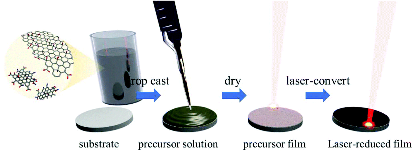 | ||
| Fig. 1 Illustration of the preparation procedures for the sample films. | ||
To ensure equal mass loading throughout the samples on the substrates prior to the laser-reduction step, the amount of applied solution was adjusted accordingly (Table 1). Solutions were either prepared in H2O or in a 1:1 mixture of N-methyl-2-pyrrolidone (NMP) and iso-propanol (i-PrOH) (NMP/i-PrOH (1:1 v/v)) to produce uniform films. When using H2O as the solvent, slow vacuum-assisted drying helped to avoid delamination during the drying process. When using NMP/i-PrOH as the solvent, drying was achieved by evaporating the solvent at an elevated temperature (∼100 °C) using a precision hotplate. Solutions with a higher CND content (>30 wt%) dried faster and tended to delaminate upon drying or laser-reduction. GO is known to swell in water and traps a substantial number of water molecules between the layers. The small CNDs also intercalate between the GO layers and, thereby, displace water molecules. Presumably, during solvent evaporation surface tension due to a drying gradient between the upper and the lower layer causes delamination.
| Sample | c(GO) (mg mL−1) | c(CND) (mg mL−1) | m(GO) (mg cm−2) | m(CND) (mg cm−2) | moverall (mg cm−2) | mass fraction CND (wt%) |
|---|---|---|---|---|---|---|
| a The concentrations of GO and CND used in the precursor solutions 1–7 are given in columns 2 and 3. The mass loading of components in a typical film for EDLCs are given in columns 4–6. The final mass fraction of CND in the solutions and the films are provided in column 7. | ||||||
| 1 | 3.63 | 0.00 | 0.51 | 0.00 | 0.51 | 0 |
| 2 | 3.63 | 0.25 | 0.48 | 0.03 | 0.51 | 6 |
| 3 | 3.63 | 0.50 | 0.45 | 0.06 | 0.51 | 12 |
| 4 | 3.63 | 1.09 | 0.39 | 0.12 | 0.51 | 23 |
| 5 | 3.63 | 1.67 | 0.35 | 0.16 | 0.51 | 32 |
| 6 | 3.63 | 3.35 | 0.27 | 0.25 | 0.51 | 48 |
| 7 | 3.63 | 6.69 | 0.18 | 0.33 | 0.51 | 65 |
The cast films were analyzed in terms of mass before and after the laser-reduction process. In general, higher laser power causes more material to be removed (evaporated) during the laser-reduction process. Detailed structural characterization and reaction mechanisms of the laser-reduction process of GO or CNDs have been published previously.22,23,26,27 In all our experiments the same laser power was used, and it was found that the investigated samples react differently upon laser impact. The precursor films with higher CND mass fractions are more stable against laser-induced evaporation (Fig. S2†). This effect is most likely caused by a synergistic influence of both GO and CNDs, which is explained based on our experimental findings in the following paragraphs. For all experiments this mass difference was taken into account and the films with equal mass loadings in regard to the final active films on the substrates were analyzed.
The laser-reduced GO/CND films were characterized by means of SEM, TEM, EELS, and Raman spectroscopy. In Fig. 2a representative SEM images of six laser-reduced samples with different mass fractions of CNDs are shown. Comparing the images reveals that increasing the mass fraction of CNDs in the precursor mixture leads to an apparent increase in the structural integrity of the films. This trend is seen throughout the samples. Higher and lower magnification images are shown in Fig. S3.† Notably, in the high CND mass fraction precursor film (6) bubble-like objects are found (Fig. S4†), that are typical of purely reduced CND phases.23,24 These patterns are presumably formed by enclosed aggregates of CNDs.
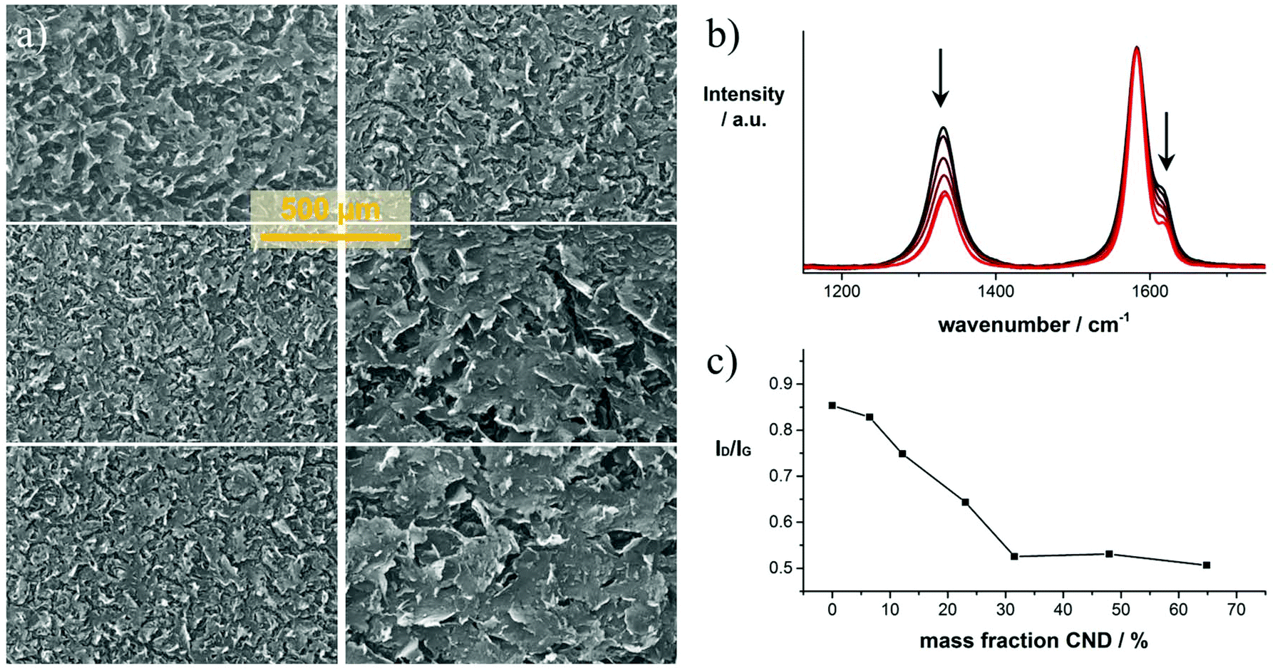 | ||
| Fig. 2 Structural characterization of laser-reduced GO/CND films; (a) low-magnification SEM images of laser-converted films of samples (1, 3, 4, 5, 6, 7) from top left down to bottom right. (b) Raman spectra of samples 1–6 (black to red) obtained upon excitation at 633 nm; (c) plot showing the D/G-intensity ratios versus the mass fraction of CNDs in the precursor solution. | ||
The graph in Fig. 2b shows a set of representative normalized Raman spectra of samples 1–6 (black to red). All spectra are composed of four major peaks assigned to the D, G, D′ and G′ bands at 1329, 1576, 1607 and 2647 cm−1, respectively. The entire spectra of representative samples are presented in Fig. S5.† In general, the pattern is similar for all tested samples. However, differences in the D-band intensity are striking. The D-band diminishes with increasing CND mass fraction until ∼65% in the precursor solution. As the D-band is related to defects within the graphitic network, we conclude that the defect density is lower when higher amounts of CNDs are present in a given sample. In the film with 70 wt% CNDs, the D-band starts to increase which is attributed to an excess of CNDs that do not interconnect with the reduced GO layers, but rather form purely reduced CND phases (Fig. S4†). The position of the G-band is maintained throughout the samples as determined by systematic fitting of the Raman spectra (Fig. S6†). Only minor shifts in the range between 1582.6 to 1583.5 cm−1 are observed, but no clear trend is found.
Deeper insights into the microscopic structure and chemical composition of the samples were obtained by TEM and EELS. In Fig. S7† representative TEM images of samples 1, 3, and 6 are shown. Samples 1 and 3 consist of flat reduced GO sheets as typically seen for reduced GO.28 Likewise, in sample 3, sheets of monolayer graphene were observed. Upon taking a closer look, blobs in a size regime of 5–10 nm on the converted carbon sheets were observed. These are not seen in sample 1, in the absence of CNDs. In sample 6, with a CND mass fraction of 48%, a significant amount of bubble-like objects stemming from the laser reduction of pure CND phases, as already shown in Fig. S4† are observed. Several spots in the tested samples were analyzed by EELS to gain information about the chemical composition. Sample 1 is composed of 99% carbon. In samples 3 and 6, traces of nitrogen and oxygen on the order of 1–4% were identified as shown in Fig. S8.† Notably, the carbon peaks in all samples show a typical graphene structure, indicating a successful conversion into graphitic/graphenic materials.
In the next step, the SSA of the laser-converted films from samples 1–7 were determined. Due to the low mass loadings of only ∼0.1 mg cm−2 the methylene blue (MB) adsorption method (see Experimental section) rather than BET measurements was chosen. The data of the MB absorption measurements are presented in Fig. S9.† As a general trend, we observe that up to a mass fraction of ∼30% CNDs, the SSA increases from 782 to 1010 m2 g−1 with an increasing amounts of CNDs in the precursor solution (Fig. 3a). This effect can be attributed to the higher structural integrity and the CNDs acting as spacers between the laser-reduced GO sheets in the reduced film. The decrease of the SSA for CND mass fractions of >40% is attributed, again, to purely reduced CND phases (Fig. S4†). Pure laser-reduced CNDs exhibit a SSA of 230 m2 g−1.23
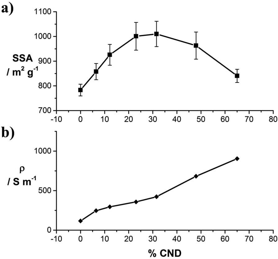 | ||
| Fig. 3 (a) Specific surface areas of 1–7 obtained by the methylene blue adsorption method; (b) sheet conductivity of samples 1–7, plotted as a function of the mass fraction of CNDs. | ||
The electrical conductivities were obtained from laser-reducing a series of films with equal mass from solutions 1–7 on defined areas of electronically insulating SiO2 wafers. The thus determined sheet conductivities are plotted in Fig. 3b. With an increasing mass fraction of CND, the conductivity increases from 118 to 904 S m−1 for samples 1 through 7, respectively. The increase follows a nearly linear trend.
The above results show improved materials’ characteristics for the laser-reduced 3D-graphene obtained from simultaneous reduction of GO and CNDs during the laser-assisted reduction process. Mechanistically, the impacting laser energy is dissipated across the GO sheets, which subsequently de-oxygenates the GO. Excess heat leads to ripping apart of the GO sheets and partial carbon removal by an oxidation/combustion process. A probable explanation is a synergistic effect of both reactive components, CNDs and GO, during the laser-induced reaction. As the GO sheets are de-oxygenated, reduced CNDs or their reaction products occurring during the laser treatment react with the reactive sites on the GO sheets and thus reduce the defects induced during laser-reduction. From the blobs observed in the TEM analysis, an interaction of this kind may be inferred. This “patching” results in a lower defect density in the 3D-carbon network. Similar effects regarding the healing of defects in GO have been observed in chemical vapor deposition experiments.39 Another positive effect on the SSA and the electrical conductivity that may be hypothesized in a mechanistic model is the improved inter-layer heat dissipation during the laser-reduction due to the presence of CNDs between the GO layers. Their presence may promote the establishment of improved interconnections between the GO layers, which leads to a milder de-oxygenation upon absorption of excess heat energy across the layers and thus, the reduction of occurring defects. At the same time, CNDs between the GO layers could act as spacers and increase the SSA during the laser-reduction by forming conductive bridges between these layers. These assumptions will require more detailed future analysis of the laser-reduced GO/CND hybrids.
The positive effect of the structural and electronic properties points to improved performance in EDLC electrodes. To test the electrochemical properties of the carbon electrodes, three-electrode electrochemical measurements were conducted with samples 1, 3, and 6. To this end, defined amounts of precursor solution were applied on top of stainless steel current collectors and subsequently laser-reduced. Fig. S11† shows the cyclic voltammograms of sample 3 in 1.0 M Na2SO4 as the electrolyte. In the tested voltage window, no apparent redox peaks were observed, indicating a purely capacitive charge storage mechanism. This is supported by the quasi-triangular shapes of the galvanostatic charge–discharge curves. In the impedance measurements shown in Fig. S11† additional evidence for the capacitive charge storage mechanism is found.
The increase in electrical conductivity and SSA upon adding CNDs is beneficial for the performance of laser-reduced GO as electrode materials in EDLCs. To quantify the effect on the electrochemical properties symmetric device assemblies of our electrodes with equal amounts of active material were tested under sealed conditions in coin cells. The active material was directly laser converted on stainless steel discs that served as the current collectors (Fig. S10†). A full characterization of the cells is shown for two example cells, produced from samples 1 (0 wt% CNDs) and 5 (32 wt% CNDs), in Fig. 4. The data of the other samples are shown in the ESI.† The mass loading of the active material on the current collector was 0.1 mg, used equally for all samples.
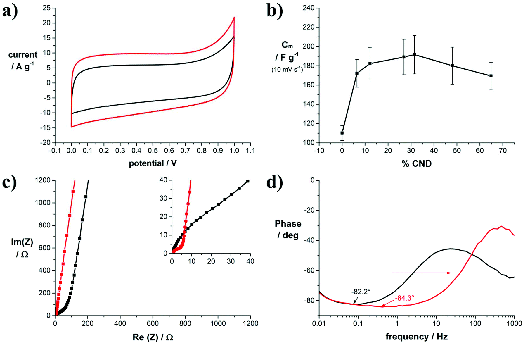 | ||
| Fig. 4 Electrochemical characterization of symmetric coin cell capacitors with different GO/CND mass ratios; (a) representative cyclic voltammograms of coin cell capacitors assembled with electrodes of 1 (black) and 5 (red) in 6.0 M KOH as the electrolyte at a scan rate of 100 mV s−1; (b) specific gravimetric capacitance versus mass fraction of CNDs contained in the precursor solution determined by cyclic voltammetry at a scan rate of 10 mV s−1; (c) representative Nyquist impedance plots of coin cell capacitors assembled with electrodes of 1 (black) and 5 (red) in 6.0 M KOH as the electrolyte; inset: zoom-in to the high-frequency region; (d) representative phase angle plots of coin cell capacitors assembled with electrodes of 1 (black) and 5 (red) in 6.0 M KOH as the electrolyte. | ||
In Fig. 4a, the mass normalized cyclic voltammograms of 1 and 5 in 6.0 M KOH are shown. Both curves have a rectangular shape typical for purely capacitive behavior. Addition of CNDs to GO in 5 leads to an increase in capacitance and a slightly improved curve shape. From the CV curves of samples 1–9 we calculated the specific gravimetric capacitance, which is plotted versus the CND mass fraction in the precursor solution in Fig. 4b. Due to rather low mass loadings on the electrodes, the measurement error is potentially high, however, a clear trend towards higher capacitance upon addition of CNDs to GO is noticeable. Maximum values are achieved with a CND mass fraction of 32%. The same trend was also observed in reference measurements using 0.5 M TBAPF6 in acetonitrile as the electrolyte (Fig. S12†). The specific capacitance in organic electrolytes is generally lower. Here, a maximum capacitance was also achieved with a CND mass fraction of 32%. The entire data set for the gravimetric capacitances determined in dependence of the scan rate are plotted in Fig. S13.†
In galvanostatic charge–discharge measurements of the same cells at different current densities (Fig. S14†), quasi-triangular curve shapes were obtained for all tested samples. Small internal resistance (IR) drops of, for example, 0.125 or 0.027 V upon discharging at 76 A g−1 for 1 or 5, respectively, are observed at the beginning of the discharge curves. From these values equivalent series resistances of 2.19 Ω or 0.47 Ω for 1 or 5 in 6.0 M KOH are obtained, respectively. Specific gravimetric capacitances determined from these charge–discharge curves (Fig. S15†) are in good agreement with the values obtained from cyclic voltammetry. Notably, the presence of CNDs also supports the cycling stability of the cells. Sample 1 exhibits excellent cycling stability with retention of the initial capacitance of 90.5% after 20000 cycles. Upon addition of a mass fraction of 32% CNDs (sample 5), a significant improvement with retention up to 98.5% after 20000 cycles is observed (Fig. S16†).
The frequency response of the cells was tested subsequently by electrochemical impedance spectroscopy. The graph in Fig. 4c compares the Nyquist plots of samples 1 and 5. Clearly, in sample 1 the high frequency region up to Re(Z) = 80 Ω is dominated by Warburg-type impedance as indicated by a 45° phase angle. The absence of this Warburg-type element in sample 5 points to a change in pore structure compared to sample 1.
The minimum phase angle of 84.3° in sample 5 is reached at a frequency of 1 Hz, while the minimum phase angle of 82.2° in sample 1 is reached at a phase angle of only 0.1 Hz. As shown in Fig. 4d, addition of CNDs to the precursor material results in lower minimum phase angles and a wider capacitive frequency region with minimum phase angles close to −90°,40 thereby widening the operative frequency region of the capacitor. As a reference, in commercial activated carbon-based EDLCs, a minimum phase angle of −85.6° was measured; however, this showed a smaller active frequency region (Fig. S17†). The improved frequency response is also reflected in the phase angle diagram presented in Fig. 4d. For example, the capacitive frequency window of the capacitors made from sample 5 is larger by more than one order of magnitude in Hz. Throughout the tested cells an improvement towards wider capacitive frequency windows is noted as shown in Fig. S18.† Typically, the frequency value at a phase angle of −45° between the resistive and the capacitive region translates to the relaxation time of the cell. This is a measure for the transition from capacitive to resistive behavior in a capacitor (RC circuit). Without the addition of CNDs, the relaxation time is 128 ms, while the lowest value measured for a CND mass fraction of 32% is 7.6 ms. Therefore, addition of CNDs to reduced GO electrodes enables operation at higher frequencies.
These trends were also observed in reference cells using an organic electrolyte. The minimum phase angles measured in the organic electrolyte are generally higher throughout all the cells. An improvement from −73.9° for sample 1 to −78.1° for samples 3 and 6 was achieved. The relaxation times improve from 100.8 ms for sample 1 to 26.9 ms for sample 5.
Conclusions
We have conducted a comprehensive study on the role of carbon nanodots (CNDs) as additives to graphene oxide (GO) in the starting material for laser-reduced GO in EDLC electrodes. In a complementary analysis of scanning electron microscopy (SEM), transmission electron microscopy (TEM), electron energy loss spectroscopy (EELS) and Raman spectroscopy, we found that the addition of CNDs to the starting material helps maintain a high structural integrity of the final 3D-graphene in the laser-assisted reduction process. Independent of the amount of CNDs, the chemical analysis yields a carbon content of >96%. Raman spectroscopy of a range of samples with different amounts of CNDs added show that the defect density in the final 3D-graphene films is significantly reduced at a CND mass fraction of ∼30%. Moreover, electrical conductivity was improved by one order of magnitude and the active surface area was enhanced by 130%. These structural improvements lead to an increase in gravimetric device capacitance from 110 to 214 F g−1 at a scan rate of 10 mV s−1 and an enhanced frequency response, determined by the minimum phase angle and the relaxation time. The simultaneous laser-reduction mechanism of graphene and carbon nanodots is currently under investigation.Experimental
Synthesis
Sample preparation
![[thin space (1/6-em)]](https://www.rsc.org/images/entities/b_char_2009.gif) :1 v/v).
17 mg of GO and different amounts of CNDs ranging from 0 to 40 mg (samples 1–10) were stirred in NMP/i-PrOH (1:1 v/v) for at least 24 h at room temperature. Defined amounts of these solutions were drop-cast on defined areas of substrates and the solvent was evaporated on a hotplate at 100 °C to ensure homogeneous drying.
:1 v/v).
17 mg of GO and different amounts of CNDs ranging from 0 to 40 mg (samples 1–10) were stirred in NMP/i-PrOH (1:1 v/v) for at least 24 h at room temperature. Defined amounts of these solutions were drop-cast on defined areas of substrates and the solvent was evaporated on a hotplate at 100 °C to ensure homogeneous drying.
The films were then reduced using a 40 W CO2 Laser engraver (Full Spectrum – glass tube laser source). To compensate for the instrument intrinsic laser intensity deviations, we conducted arrays of experiments, all on the same day and under the same conditions. However, some stray results due to the laser instrument cannot be ruled out.
Microscopy
Scanning electron microscopy (SEM) was conducted on a JEOL JSM-6700F with an electron acceleration voltage of 3 kV. Samples were prepared on either stainless steel or SiO2 substrates.Transmission electron microscopy (TEM) and electron energy loss spectroscopy (EELS) were conducted using a double-cs-corrected Jeol ARM200F, equipped with a cold field emission gun. The acceleration voltage was put to 200 kV, the emission was set to 5 μA and a condenser aperture with a diameter of 150 μm was used. Samples were transferred by dipping the Lacey carbon grid onto the as-prepared laser-reduced films.
Determination of the ID/IG-ratios
Raman spectra were recorded with a Renishaw InVia Raman Microscope. For each sample 16 Raman spectra were recorded in mapping mode. The separation between the spots was 10 μm. The obtained spectra were baseline corrected and averaged using Wire 3.4 software. The D and G-band regions between 1150 and 1750 cm−1 of the averaged spectra were fit with three Lorentzians.Determination of the sheet conductivity
Defined amounts of precursor solutions were drop-cast on a defined area (5 × 17 mm) of an insulating SiO2 substrate. After evaporation of the solvent, the films were laser-reduced. The short ends of the films were connected to measure the resistance of the films. From the resistance of the films, the sheet resistance was determined using the thickness and the area of the films. The lead and contact resistance from the probing electrodes was neglected as they were two orders of magnitude smaller than the resistance of the film.Determination of the active surface area
The GO/CND films were laser-reduced on substrates with defined areas and the mass was determined. The substrates with the laser-reduced films were immersed into solutions of methylene blue (MB) in DI water with known concentrations and stirred vigorously. After 24 h the solutions were centrifuged at 16000 rpm to remove any suspended material.43 The number of MB molecules adsorbed onto the surfaces was calculated from the difference in absorption at 665 nm with respect to the reference solution. Every MB molecule is assumed to occupy 1.35 nm2 of the active surface area.44 For all experiments involving MB, polypropylene beakers and vials were used. The spectra are shown in Fig. S9.†
Electrochemical measurements
All electrochemical measurements were performed with a Biologic VMP3 electrochemical workstation.Solution-based measurements were conducted with a three-electrode setup using an Ag/AgCl reference electrode and platinum foil as a counter electrode. The active material was applied on a stainless steel strip which was used as the working electrode.
Quantitative measurements were conducted in a symmetric device geometry. Cyclic voltammetry, charge–discharge curves, and electrochemical impedance spectroscopy was recorded with a Biologic VMP3 electrochemical workstation. Symmetric electrochemical capacitors were assembled in coin cells with electrode diameters of 15 mm and tested under sealed conditions.
 by the volume of the film V, the scan rate ν and the potential scan range (E1 − E0).
Conflicts of interest
There are no conflicts to declare.Acknowledgements
This work was supported by the Deutsche Forschungsgemeinschaft (German Academic Research Society), grant number STR1508/1-2 (V. S.) and the Dr Myung Ki Hong Endowed Chair in Materials Innovation (R. B. K.). We thank the microscopy facility in the UCLA Department of Materials Science and Engineering led by Dr S. V. Prikhodko for use of their Raman spectrometer.References
- V. Georgakilas, J. a. Perman, J. Tucek and R. Zboril, Chem. Rev., 2015, 115, 4744–4822 CrossRef CAS PubMed.
- J. K. Wassei and R. B. Kaner, Acc. Chem. Res., 2013, 46, 2244–2253 CrossRef CAS PubMed.
- M. F. El-Kady, Y. Shao and R. B. Kaner, Nat. Rev. Mater., 2016, 1, 16033 CrossRef CAS.
- Nanocarbons for Advanced Energy Storage, ed. X. Feng, Wiley-VCH Verlag GmbH & Co. KGaA, Weinheim, Germany, 2015 Search PubMed.
- Y. Sun, Q. Wu and G. Shi, Energy Environ. Sci., 2011, 4, 1113 RSC.
- Y. Shao, M. F. El-Kady, L. J. Wang, Q. Zhang, Y. Li, H. Wang, M. F. Mousavi and R. B. Kaner, Chem. Soc. Rev., 2015, 44, 3639–3665 RSC.
- S. He and W. Chen, Nanoscale, 2015, 7, 6957–6990 RSC.
- X. Yao and Y. Zhao, Chem, 2017, 2, 171–200 CAS.
- S. Han, D. Wu, S. Li, F. Zhang and X. Feng, Adv. Mater., 2014, 26, 849–864 CrossRef CAS PubMed.
- A.-H. Lu, G.-P. Hao, Q. Sun, X.-Q. Zhang and W.-C. Li, in Chemical Synthesis and Applications of Graphene and Carbon Materials, Wiley-VCH Verlag GmbH & Co. KGaA, Weinheim, Germany, 2016, pp. 115–157 Search PubMed.
- Chemical Synthesis and Applications of Graphene and Carbon Materials, ed. M. Antonietti and K. Müllen, Wiley-VCH Verlag GmbH & Co. KGaA, Weinheim, Germany, 2017 Search PubMed.
- H. Zhan, D. J. Garrett, N. V. Apollo, K. Ganesan, D. Lau, S. Prawer and J. Cervenka, Sci. Rep., 2016, 6, 19822 CrossRef CAS PubMed.
- Z. Chen, W. Ren, L. Gao, B. Liu, S. Pei and H.-M. Cheng, Nat. Mater., 2011, 10, 424–428 CrossRef CAS PubMed.
- Y. Wang, L. Tao, Z. Xiao, R. Chen, Z. Jiang and S. Wang, Adv. Funct. Mater., 2018, 28, 1705356 CrossRef.
- S. Dou, X. Wang and S. Wang, Small Methods, 2018, 1800211 Search PubMed.
- D. Liu, L. Tao, D. Yan, Y. Zou and S. Wang, ChemElectroChem, 2018, 5, 1775–1785 CrossRef CAS.
- Y. Xu, K. Sheng, C. Li and G. Shi, ACS Nano, 2010, 4, 4324–4330 CrossRef CAS PubMed.
- X.-F. Jiang, X.-B. Wang, P. Dai, X. Li, Q. Weng, X. Wang, D.-M. Tang, J. Tang, Y. Bando and D. Golberg, Nano Energy, 2015, 16, 81–90 CrossRef CAS.
- D. Ge, L. Yang, L. Fan, C. Zhang, X. Xiao, Y. Gogotsi and S. Yang, Nano Energy, 2015, 11, 568–578 CrossRef CAS.
- J. Lin, Z. Peng, Y. Liu, F. Ruiz-Zepeda, R. Ye, E. L. G. Samuel, M. J. Yacaman, B. I. Yakobson and J. M. Tour, Nat. Commun., 2014, 5, 5714 CrossRef CAS PubMed.
- M. F. El-Kady, V. Strong, S. Dubin and R. B. Kaner, Science, 2012, 335, 1326–1330 CrossRef CAS PubMed.
- V. Strong, S. Dubin, M. F. El-Kady, A. Lech, Y. Wang, B. H. Weiller and R. B. Kaner, ACS Nano, 2012, 6, 1395–1403 CrossRef CAS PubMed.
- V. Strauss, K. Marsh, M. D. Kowal, M. F. El-Kady and R. B. Kaner, Adv. Mater., 2018, 30, 1704449 CrossRef PubMed.
- V. Strauss, M. Anderson, C. L. Turner and R. B. Kaner, Mater. Today Energy, 2019, 11, 114–119 CrossRef.
- V. Strauss, M. Anderson, C. Wang, A. Borenstein and R. B. Kaner, Small, 2018, 1803656 CrossRef PubMed.
- A. Borenstein, V. Strauss, M. D. Kowal, M. Yoonessi, M. Muni, M. Anderson and R. B. Kaner, J. Mater. Chem. A, 2018, 6, 20463–20472 RSC.
- K. Griffiths, C. Dale, J. Hedley, M. D. Kowal, R. B. Kaner and N. Keegan, Nanoscale, 2014, 6, 13613–13622 RSC.
- R. Kumar, R. K. Singh, D. P. Singh, E. Joanni, R. M. Yadav and S. A. Moshkalev, Coord. Chem. Rev., 2017, 342, 34–79 CrossRef CAS.
- Y.-Q. Dang, S.-Z. Ren, G. Liu, J. Cai, Y. Zhang and J. Qiu, Nanomaterials, 2016, 6, 212 CrossRef PubMed.
- Q. Li, H. Cheng, X. Wu, C.-F. F. Wang, G. Wu and S. Chen, J. Mater. Chem. A, 2018, 6, 14112–14119 RSC.
- G. Yuan, X. Zhao, Y. Liang, L. Peng, H. Dong, Y. Xiao, C. Hu, H. Hu, Y. Liu and M. Zheng, J. Colloid Interface Sci., 2019, 536, 628–637 CrossRef CAS PubMed.
- S. Bak, D. Kim and H. Lee, Curr. Appl. Phys., 2016, 16, 1192–1201 CrossRef.
- M. Nováček, O. Jankovský, J. Luxa, D. Sedmidubský, M. Pumera, V. Fila, M. Lhotka, K. Klímová, S. Matějková and Z. Sofer, J. Mater. Chem. A, 2017, 5, 2739–2748 RSC.
- Graphene Oxide, ed. A. M. Dimiev and S. Eigler, John Wiley & Sons, Ltd, Chichester, UK, 2016 Search PubMed.
- D. Konios, M. M. Stylianakis, E. Stratakis and E. Kymakis, J. Colloid Interface Sci., 2014, 430, 108–112 CrossRef CAS PubMed.
- F. Baskoro, C.-B. Wong, S. R. Kumar, C.-W. Chang, C.-H. Chen, D. W. Chen and S. J. Lue, J. Membr. Sci., 2018, 554, 253–263 CrossRef CAS.
- V. Strauss, J. T. Margraf, C. Dolle, B. Butz, T. J. Nacken, J. Walter, W. Bauer, W. Peukert, E. Spiecker, T. Clark and D. M. Guldi, J. Am. Chem. Soc., 2014, 136, 17308–17316 CrossRef CAS PubMed.
- P. Yu, X. Wen, Y.-R. Toh, Y.-C. Lee, K.-Y. Huang, S. Huang, S. Shrestha, G. Conibeer and J. Tang, J. Mater. Chem. C, 2014, 2, 2894 RSC.
- S. Grimm, M. Schweiger, S. Eigler and J. Zaumseil, J. Phys. Chem. C, 2016, 120, 3036–3041 CrossRef CAS.
- A. Noori, M. F. El-Kady, M. S. Rahmanifar, R. B. Kaner and M. F. Mousavi, Chem. Soc. Rev., 2019, 48, 1272–1341 RSC.
- J. T. Margraf, F. Lodermeyer, V. Strauss, P. Haines, J. Walter, W. Peukert, R. D. Costa, T. Clark and D. M. Guldi, Nanoscale Horiz., 2016, 1, 220–226 RSC.
- V. Strauss, A. Kahnt, E. M. Zolnhofer, K. Meyer, H. Maid, C. Placht, W. Bauer, T. J. Nacken, W. Peukert, S. H. Etschel, M. Halik and D. M. Guldi, Adv. Funct. Mater., 2016, 26, 7975–7985 CrossRef CAS.
- S. Naeem, V. Baheti, J. Wiener and J. Marek, J. Text. Inst., 2017, 108, 803–811 CrossRef CAS.
- P. T. Hang, Clays Clay Miner., 1970, 18, 203–212 CrossRef.
Footnote |
| † Electronic supplementary information (ESI) available. See DOI: 10.1039/c9nr01719d |
| This journal is © The Royal Society of Chemistry 2019 |