
 Open Access Article
 This Open Access Article is licensed under a Creative Commons Attribution-Non Commercial 3.0 Unported Licence
Fully inkjet printed ultrathin microsupercapacitors based on graphene electrodes and a nano-graphene oxide electrolyte†
Szymon
Sollami Delekta
 a,
Karin H.
Adolfsson
b,
Nejla
Benyahia Erdal
b,
Minna
Hakkarainen
b,
Mikael
Östling
a and
Jiantong
Li
*a
a,
Karin H.
Adolfsson
b,
Nejla
Benyahia Erdal
b,
Minna
Hakkarainen
b,
Mikael
Östling
a and
Jiantong
Li
*a
aKTH Royal Institute of Technology, School of Electrical Engineering and Computer Science, Division of Electronics, Electrum 229, SE-164 40 Kista, Sweden. E-mail: jiantong@kth.se
bKTH Royal Institute of Technology, Department of Fibre and Polymer Technology, Teknikringen 58, SE 11428 Stockholm, Sweden
First published on 2nd May 2019
Abstract
The advance of miniaturized and low-power electronics has a striking impact on the development of energy storage devices with constantly tougher constraints in terms of form factor and performance. Microsupercapacitors (MSCs) are considered a potential solution to this problem, thanks to their compact device structure. Great efforts have been made to maximize their performance with new materials like graphene and to minimize their production cost with scalable fabrication processes. In this regard, we developed a full inkjet printing process for the production of all-graphene microsupercapacitors with electrodes based on electrochemically exfoliated graphene and an ultrathin solid-state electrolyte based on nano-graphene oxide. The devices exploit the high ionic conductivity of nano-graphene oxide coupled with the high electrical conductivity of graphene films, yielding areal capacitances of up to 313 μF cm−2 at 5 mV s−1 and high power densities of up to ∼4 mW cm−3 with an overall device thickness of only ∼1 μm.
The advance of ever-shrinking and low-power electronic devices such as soft and implantable electronics, wireless sensor networks, wearable displays, nanorobotics and micro-electromechanical systems (MEMS) is driving the development of new miniaturized and ultrathin energy storage solutions to ensure their energetic autonomy.1–3 Among power sources, supercapacitors (SCs) are prime candidates for these applications, thanks to their high power density, long cycle life and safe operation,4 but they are commonly fabricated by stacking their components in a bulky form factor.5 The efforts for miniaturization of SCs have attracted ample research interest recently,6,7 leading to the expansion of a new class of SCs, microsupercapacitors (MSCs),8,9 which boast high volumetric performances compared to their stacked counterparts.8,10 This improvement is mainly on account of their planar design with the electrodes closely spaced and naturally separated, thus decreasing the ion diffusion lengths, increasing the fraction of the active materials and eliminating the need for a separator.11,12 In order to further increase their compactness, integrability and compatibility with various substrates, ultrathin MSCs with a minimized device thickness in the order of ∼μm or below are highly desired, where the active materials need to be carefully selected and optimized.13,14 At present, most of the research on MSCs is focused on the development of high-performance electrode materials,15 and among them, graphene stands out, thanks to its high in-plane electrical conductivity, large surface area and high intrinsic capacitance given by its 2D structure.16–18 Because the electrodes are typically submerged in liquid or gel electrolyte, the final device ends up being unnecessarily bulky as the thickness of the electrolyte cannot be controlled accurately or packaging is required to prevent leakage.18 A better solution is the use of a solid-state electrolyte, which can be self-contained and deposited as a thin film. Also, the fabrication of ultrathin MSCs requires good deposition accuracy and thickness control while being scalable and reproducible. In this regard, inkjet printing is a promising deposition technique, thanks to its attractive features such as good resolution (down to 50 μm), direct patterning, scalability, cost-effectiveness, low material usage and, most importantly, good thickness control.19,20 Furthermore, the compatibility of inkjet printing with several functional materials has led to the realization of “all-printed” energy storage devices, which significantly improves the scalability and resolution because no manual assembly step (e.g. electrolyte drop-casting or electrochemical cell assembly) is needed during the device fabrication. As a matter of fact, we previously printed hundreds of MSCs and integrated them into a large-scale array which can be simultaneously charged up to 12 V.21 However, to achieve good electrochemical performance, the electrolytes needed to be printed with a thickness of ∼100 μm because of the relatively low ionic conductivity of the gel electrolytes. In this respect, graphene oxide (GO) is a good candidate for solid-state electrolytes because it contains abundant oxygen groups that facilitate ion transport and lead to high ionic conductivity,22,23 making it possible to achieve good electrochemical performance with ultrathin electrolyte layers.
In this work, we present a full inkjet printing process for the fabrication of all-graphene microsupercapacitors with an ultrathin solid-state electrolyte based on nano-graphene oxide (nGO), a form of graphene oxide with lateral dimensions at the nanoscale.24 Moreover, thanks to its excellent dispersibility resulting from small particle size, nGO is remarkably suitable for inkjet printing, enabling accurate thickness control of the printed thin film. As a result, the volumetric performance can be maximized by minimizing the thickness and volume of the electrolyte, producing ultrathin (overall device thickness ∼1 μm) devices with high energy and power densities.
The all-graphene MSCs consist of interdigitated electrodes based on electrochemically exfoliated graphene (EG) and a nGO-based electrolyte. The ink formulation process and the MSC fabrication are described in Experimental methods, ESI, and in the schematic in Fig. S1.† Briefly, to fabricate the electrodes, the EG inks were formulated as previously reported21 and printed on flexible Kapton substrates to form the interdigitated electrodes, followed by a brief annealing step to remove the binder (ethyl cellulose). Next, the electrolyte was produced by inkjet printing the nGO inks. The nanodispersions of nGO were derived from cellulose through a microwave-assisted process as reported previously,25,26 exhibiting a C/O ratio of ∼2.1 (see X-ray photoelectron spectroscopy analysis, ESI, and Fig. S3†). Because the so-obtained nGO has a small particle size and the oxygen-containing groups (C–OH, C–O, COO–H and C![[double bond, length as m-dash]](https://www.rsc.org/images/entities/char_e001.gif) O) are located on the edges and surface of the nanosheets,27 it has a very high dispersibility and colloidal stability in a range of solvents, especially water.28,29 As a result, we were able to obtain stable inks containing highly concentrated nGO (20 mg ml−1) in a mixture of deionized water, ethylene glycol and concentrated phosphoric acid (H3PO4). The inks are stable (without any sedimentation) for at least several months. Their stability was also confirmed by zeta potential measurements where, even after the addition of ethylene glycol and H3PO4, the nGO exhibited negative charge which increases the colloidal stability by preventing flake coagulation (Fig. S4†).30 Thanks to their colloidal stability, the nGO inks exhibited ideal jetting performance (Fig. S5†) which enabled reliable inkjet printing at a resolution down to around 50 μm. The deposited nGO thin film exhibits high ionic conductivity due to the water molecules adsorbing onto its surface30–32 (Fig. S6a†) and becomes solid-state after drying, indicating that the devices do not suffer from leakage. By adding H3PO4 into the material, we were able to increase its ionic conductivity to ∼3 mS cm−1 (Fig. S6b†).
O) are located on the edges and surface of the nanosheets,27 it has a very high dispersibility and colloidal stability in a range of solvents, especially water.28,29 As a result, we were able to obtain stable inks containing highly concentrated nGO (20 mg ml−1) in a mixture of deionized water, ethylene glycol and concentrated phosphoric acid (H3PO4). The inks are stable (without any sedimentation) for at least several months. Their stability was also confirmed by zeta potential measurements where, even after the addition of ethylene glycol and H3PO4, the nGO exhibited negative charge which increases the colloidal stability by preventing flake coagulation (Fig. S4†).30 Thanks to their colloidal stability, the nGO inks exhibited ideal jetting performance (Fig. S5†) which enabled reliable inkjet printing at a resolution down to around 50 μm. The deposited nGO thin film exhibits high ionic conductivity due to the water molecules adsorbing onto its surface30–32 (Fig. S6a†) and becomes solid-state after drying, indicating that the devices do not suffer from leakage. By adding H3PO4 into the material, we were able to increase its ionic conductivity to ∼3 mS cm−1 (Fig. S6b†).
The inkjet printing technique enables the fabrication of devices with arbitrary geometry and thickness. The devices were printed with a finger length of 1.9 mm, a finger width of 550 μm, an 8 finger and inter-finger gap of 350 μm, with a geometrical area of 0.16 cm2 (excluding finger gaps) and a footprint area (area covered by the electrolyte) of 0.24 cm2 (Fig. 1a). Scanning electron microscopy (SEM) was used to investigate the morphology of the printed films as shown in Fig. 1b and c. The surface of the bare graphene electrode (Fig. 1b) exhibits the sharp protruding edges of the graphene flakes, a typical trait of printed graphene films which contributes to maximizing their surface area. On the other hand, the printed nGO (Fig. 1c) appears as a uniform and conformal coating fully covering the underlying graphene layer. Even the edges of the graphene flakes seem to be covered by nGO, indicating a large contact area between the electrode and electrolyte. The nGO can be observed in the TEM image (Fig. 1d), where the nanoparticles appear to be mostly spherical with an average diameter of 60 nm although somewhat agglomerated. To investigate the influence of the volume on the device performance, the thicknesses of both the electrode and electrolyte were varied by controlling the number of printing passes of the inkjet printed layers. The devices were named according to the number of printing passes, so e.g. the EG20L/nGO20L device consists of 20 printing passes of EG and 20 printing passes of nGO. The corresponding thicknesses of the electrodes were found to be about 30, 50, and 100 nm for 5L, 10L and 20L, respectively, while the electrolyte thickness was around 0.5, 1.0, 1.3 and 1.6 μm for 5L, 10L, 20L and 30L, respectively (Fig. S7†). We could observe that for both EG and GO patterns, the thickness increases almost linearly with the number of printing passes (Fig. 2a) and that the profiles of the printed films are uniform with negligible coffee-ring effects, which causes non-uniform thickness between the center and perimeter of the printed patterns.33 Cyclic voltammetry (CV), galvanostatic charge–discharge (GCD) and electrochemical impedance spectroscopy (EIS) were performed to characterize the performance of the devices. Fig. 2b shows the CV curves of the EG20L/nGO20L device at scan rates of up to 50 mV s−1. The device exhibits rectangular CV curves indicating ideal electric double layer capacitive behavior. As shown in Fig. S8†, this behavior continues at higher scan rates albeit with elongated CV curves caused, as expected, by a less efficient ion migration to the electrodes. The thickness of both the electrolyte (Fig. 2c) and electrode (Fig. 2d) plays a significant role in the CV performance of the devices and a summary of the extracted areal capacitances can be found in Fig. 2e and f, respectively. Although the device with the thinnest electrolyte (5L) showed a slightly resistive and lens-shaped CV curve with an areal capacitance (CA) of around 200 μF cm−2 (at 5 mV s−1), the behavior improves significantly for thicker nGO films. It is found that the optimal amount of the printing passes of the electrolyte is 20L (CA = 313 μF cm−2 at 5 mV s−1) because thicker films yield similar capacitances within the studied scan rate range, indicating an overabundance of the electrolyte. The observations from the CV curves are confirmed by the results of the GCD measurements. Fig. 3a and b show the GCD performance of the EG20L/nGO20L device at various current densities, exhibiting a triangular and symmetric response to charging and discharging, respectively. This confirms that the energy storage mechanism is based on the electrical double layer capacitance with an ideal capacitive behavior. The GCD curves of the devices (Fig. 3c and d) yield areal capacitances (Fig. 3e and f) in agreement with the CV measurements. Finally, we also performed GCD cycling for 11![[thin space (1/6-em)]](https://www.rsc.org/images/entities/char_2009.gif) 000 cycles on the EG20L/nGO20L device, showing a good capacitance retention of >65% (Fig. S9a†), although some fluctuation can be observed after the 6000th cycle due to slight variations of humidity.
000 cycles on the EG20L/nGO20L device, showing a good capacitance retention of >65% (Fig. S9a†), although some fluctuation can be observed after the 6000th cycle due to slight variations of humidity.
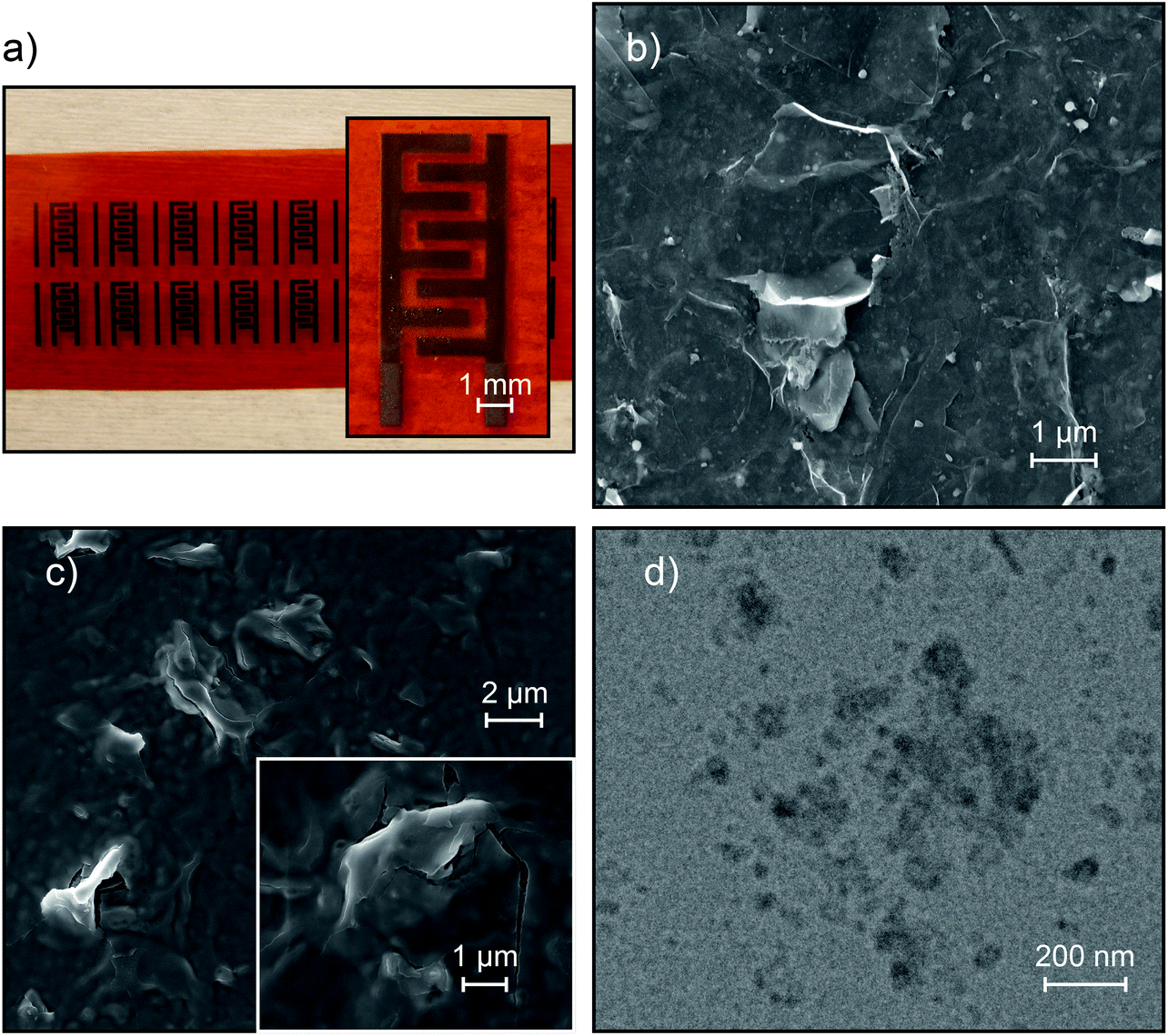 | ||
| Fig. 1 Optical and electron microscopy images of the fully inkjet printed all-graphene microsupercapacitors. (a) Optical image of the inkjet printed all-graphene microsupercapacitors. (b) SEM image of the graphene electrode with the protruding graphene flakes and binder residue visible. (c) SEM image of the printed nGO electrolyte on top of the graphene film. The inset shows a graphene flake fully covered with nGO. (d) TEM image of the nGO showing an average particle diameter of 60 nm. | ||
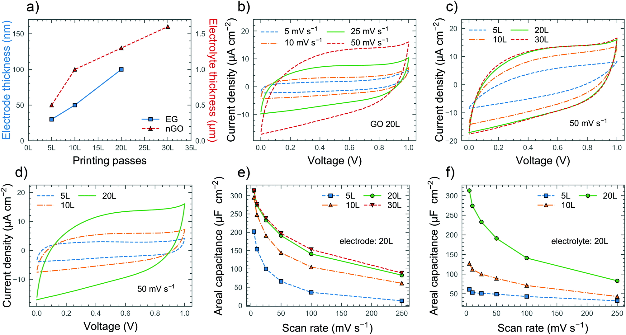 | ||
| Fig. 2 Cyclic voltammetry (CV) performance of the fully inkjet printed all-graphene microsupercapacitors. (a) Electrode and electrolyte thickness compared to the number of printing passes. (b) CV curves of the EG20L/nGO20L device at different scan rates. (c) CV performance of devices with 20L of EG electrodes and varying thicknesses of nGO electrolyte at 50 mV s−1. (d) CV curves of devices with 20L of nGO electrolyte and varying thicknesses of EG electrode at 50 mV s−1. (e, f) Areal capacitances extracted from the CV curves with varying electrolyte and electrode thicknesses at various scan rates. | ||
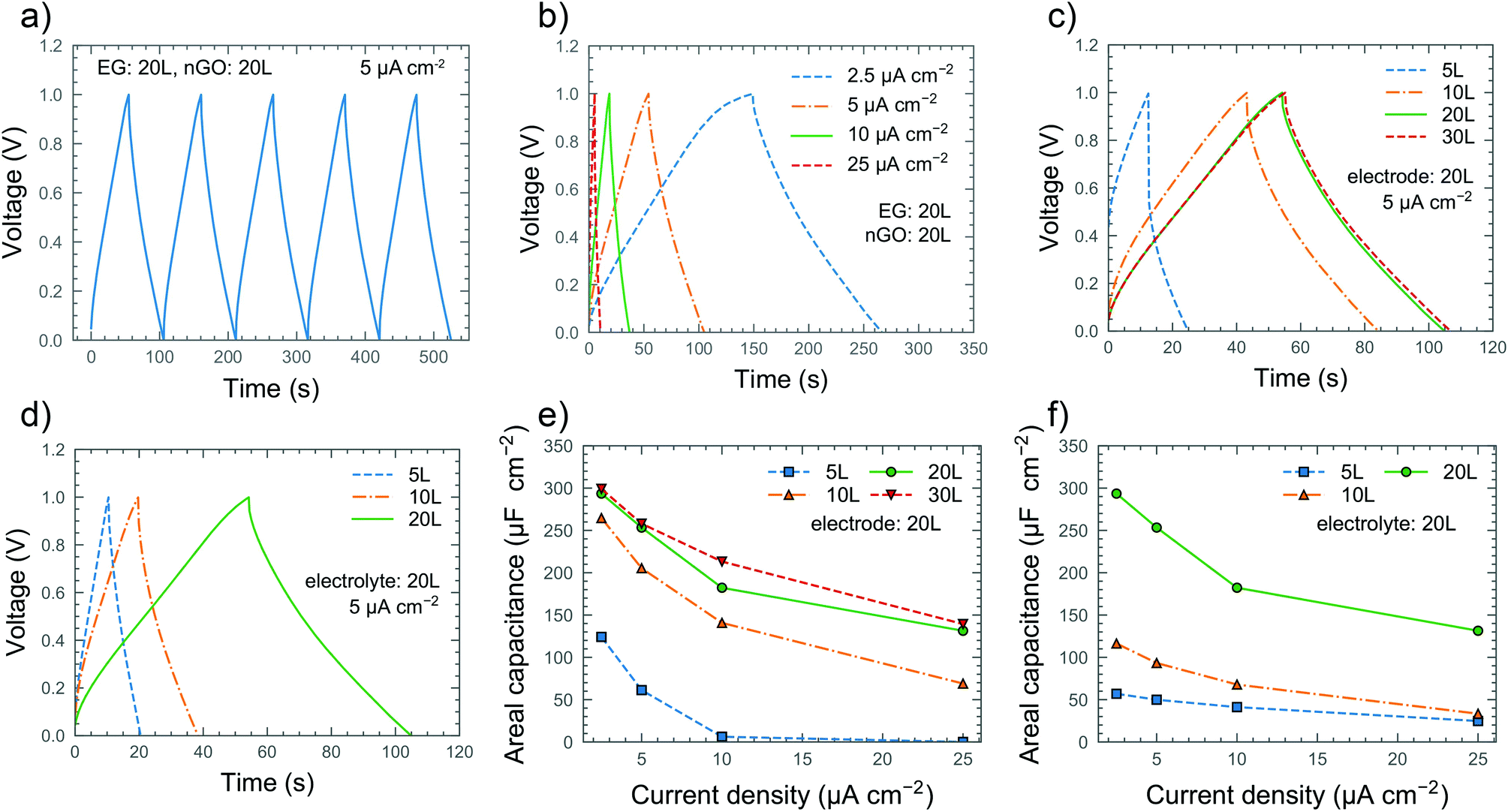 | ||
| Fig. 3 Galvanostatic charge–discharge (GCD) performance of the printed microsupercapacitors. (a) GCD curves of the EG20L/nGO20L device at 5 μA cm−2. (b) GCD performance of the EG20L/nGO20L device at various current densities. (c, d) Effect of electrolyte (c) and electrode (d) thickness on GCD performance at 5 μA cm−2. (e, f) Summary of the areal capacitances extracted from the GCD curve showing the influence of the electrolyte (e) and electrode (f) thickness on the performance of the devices. | ||
To confirm our previous remarks on the dependence of electrolyte thickness on ionic conductivity, we performed EIS measurements on all of the devices (Fig. S9b†) and measured their equivalent series resistance (ESR) corresponding to the intercept of the semicircle from EIS. The results confirm that although the ionic conductance generally increases with the electrolyte thickness, the increase is not linear for thicker films and 30 printing passes of electrolyte end up with similar ESRs to 20 passes. Fig. 4a summarizes the areal energy and power densities of our devices, showing that the EG20L/nGO20L and EG20L/nGO30L devices have the highest performance, especially when compared to a reference device with EG20L as the electrode and drop-cast polyvinyl alcohol (PVA)/H3PO4 as the electrolyte.
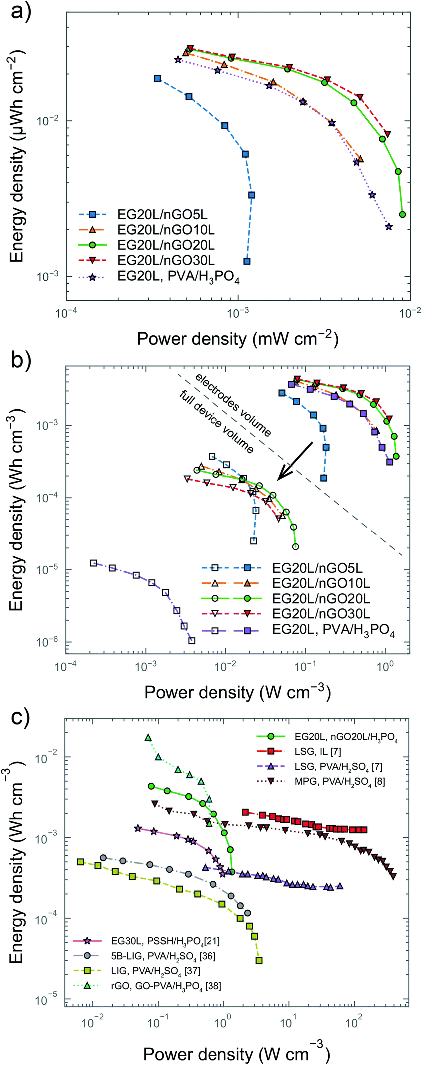 | ||
| Fig. 4 Ragone plots of microsupercapacitors (MSCs). (a) Areal energy and power densities of our MSCs. (b) Volumetric energy and power densities of our MSCs, showing the difference in performance depending on whether just the volume of the electrodes is considered or the full volume of the device. These values are also reported in Table S1.† (c) Volumetric performance comparison between our best MSC (green line, circular markers) and recently reported MSCs in the literature7,8,21,36–38 with their electrode material and electrolyte being shown. In all plots, hollow markers denote that the whole device volume was accounted for when extracting the metrics, while filled markers refer to metrics extracted from the electrode volume only. | ||
Volumetric figures-of-merit are often overlooked but essential for reporting the true performance of SCs in a reliable way,34 especially when envisioning the device for practical applications. In this respect, the footprint of all the components of the device should be considered (e.g. electrodes, electrolyte, separator, current collectors and packaging) as they significantly affect the overall device performance.35 In the case of microdevices, the weight of a thin film of the electrode material is negligible and their gravimetric performances do not scale up linearly with the thickness of the electrode, making these metrics potentially misleading.10 Volumetric energy and power densities are generally less vulnerable to these uncertainties, but they also depend on what component is included, as can also be seen in the case of our devices. We illustrate how the volumetric performance depends on the device components in Fig. 4b. The hollow markers in the Ragone plot refer to the power (Pd,full) and energy densities (Ed,full) of the full volume of the device (including the volume of the electrolyte) and filled markers only include the volume of the two electrodes (Ed,el and Pd,el – excluding finger gaps). It can be seen that the EG20L/nGO20L MSC exhibits an Ed,full value of ∼0.2 mW h cm−3 with a corresponding Pd,full value of ∼4 mW cm−3. Both of these figures increase by a factor of more than 10 when just the volume of the electrodes is considered, a trend which is common in all of our devices. For comparison, we also studied a MSC with a typical drop-cast PVA/H3PO4 electrolyte. Because drop-casting yields poor control on the uniformity and thickness of the electrolyte layers, the PVA-based electrolyte exhibits a thickness higher than 20 μm. However, the corresponding device can barely attain comparable Ed,el and Pd,el to our nGO-based devices, whereas Ed,full and Pd,full are significantly (more than one order of magnitude) lower (Fig. 4b), indicating that our fully printed solution is the most space efficient. The volumetric performances of our devices are in line with MSCs reported recently in the literature (Fig. 4c), indicating that our technique has the potential for fabricating high-performance energy storage devices.
Conclusions
In conclusion, we have demonstrated a full inkjet printing technique for the fabrication of all-graphene micro-supercapacitors. Our devices are composed of inkjet printed graphene films – constituting the current collectors and active electrodes – and inkjet printed nano-graphene oxide (nGO) – constituting the electrolyte. By making use of the high ionic conductivity and hygroscopicity of nGO, we could obtain areal capacitances of up to 313 μF cm−2 at 5 mV s−1 at an overall device thickness of about 1 μm. To maximize the performance over the volume of our devices, we have systematically explored the influence of the device thickness on the performance. As a result, the ultrathin devices obtain power densities and energy densities comparable to devices with thick or liquid electrolytes. Thanks to its attractive features such as high scalability and cost-effectiveness along with no requirement of manual assembly steps and bulky inactive components, we believe that our fully inkjet printed technique can gain full advantage out of graphene. The high performance coupled with a compact form factor might make our devices viable power sources for miniaturized electronics.Conflicts of interest
There are no conflicts to declare.Acknowledgements
We would like to acknowledge the financial support of the Swedish Research Council through the Framework project (no. 2014-6160) and the Marie Skłodowska Curie International Career Grant (no. 2015-00395, co-funded by Marie Skłodowska-Curie Actions, through the Project INCA 600398), the Formas Foundation through the Future Research Leaders Grant (no. 2016-00496), the ÅForsk Foundation (through Grant no. 17-352), the Olle Engkvist Byggmästare Foundation (through Research Project no. 2014/799) and KTH Sustainability (through the Grant V-2017-0540).References
- M. Beidaghi and Y. Gogotsi, Energy Environ. Sci., 2014, 7, 867 RSC
.
- C. Wang, K. Sim, J. Chen, H. Kim, Z. Rao, Y. Li, W. Chen, J. Song, R. Verduzco and C. Yu, Adv. Mater., 2018, 30, 1706695 CrossRef
- J. Kim, H. J. Shim, J. Yang, M. K. Choi, D. C. Kim, J. Kim, T. Hyeon and D.-H. Kim, Adv. Mater., 2017, 29, 1700217 CrossRef
- A. González, E. Goikolea, J. A. Barrena and R. Mysyk, Renewable Sustainable Energy Rev., 2016, 58, 1189–1206 CrossRef
- K.-H. Choi, D. B. Ahn and S.-Y. Lee, ACS Energy Lett., 2018, 3, 220–236 CrossRef CAS
- P. Huang, C. Lethien, S. Pinaud, K. Brousse, R. Laloo, V. Turq, M. Respaud, A. Demortiere, B. Daffos, P. L. Taberna, B. Chaudret, Y. Gogotsi and P. Simon, Science, 2016, 351, 691–695 CrossRef CAS PubMed
- M. F. El-Kady and R. B. Kaner, Nat. Commun., 2013, 4, 1475 CrossRef PubMed
- Z. Wu, K. Parvez, X. Feng and K. Müllen, Nat. Commun., 2013, 4, 2487 CrossRef PubMed
- H. Xiao, Z.-S. Wu, L. Chen, F. Zhou, S. Zheng, W. Ren, H.-M. Cheng and X. Bao, ACS Nano, 2017, 11, 7284–7292 CrossRef CAS PubMed
- J. Chmiola, C. Largeot, P. L. Taberna, P. Simon and Y. Gogotsi, Science, 2010, 328, 480–483 CrossRef CAS
- G. Sun, J. An, C. K. Chua, H. Pang, J. Zhang and P. Chen, Electrochem. Commun., 2015, 51, 33–36 CrossRef CAS
- C. Couly, M. Alhabeb, K. L. Van Aken, N. Kurra, L. Gomes, A. M. Navarro-Suárez, B. Anasori, H. N. Alshareef and Y. Gogotsi, Adv. Electron. Mater., 2018, 4, 1700339 CrossRef
- L. Peng, X. Peng, B. Liu, C. Wu, Y. Xie and G. Yu, Nano Lett., 2013, 13, 2151–2157 CrossRef CAS PubMed
- S. Sollami Delekta, M. Östling and J. Li, ACS Appl. Energy Mater., 2019, 2, 158–163 CrossRef CAS
- Z. Yu, L. Tetard, L. Zhai and J. Thomas, Energy Environ. Sci., 2015, 8, 702–730 RSC
- A. C. Ferrari, F. Bonaccorso, V. Fal'ko, K. S. Novoselov, S. Roche, P. Bøggild, S. Borini, F. H. L. Koppens, V. Palermo, N. Pugno, J. A. Garrido, R. Sordan, A. Bianco, L. Ballerini, M. Prato, E. Lidorikis, J. Kivioja, C. Marinelli, T. Ryhänen, A. Morpurgo, J. N. Coleman, V. Nicolosi, L. Colombo, A. Fert, M. Garcia-Hernandez, A. Bachtold, G. F. Schneider, F. Guinea, C. Dekker, M. Barbone, Z. Sun, C. Galiotis, A. N. Grigorenko, G. Konstantatos, A. Kis, M. Katsnelson, L. Vandersypen, A. Loiseau, V. Morandi, D. Neumaier, E. Treossi, V. Pellegrini, M. Polini, A. Tredicucci, G. M. Williams, B. Hee Hong, J.-H. Ahn, J. Min Kim, H. Zirath, B. J. van Wees, H. van der Zant, L. Occhipinti, A. Di Matteo, I. A. Kinloch, T. Seyller, E. Quesnel, X. Feng, K. Teo, N. Rupesinghe, P. Hakonen, S. R. T. Neil, Q. Tannock, T. Löfwander and J. Kinaret, Nanoscale, 2015, 7, 4598–4810 RSC
- M. F. El-Kady, Y. Shao and R. B. Kaner, Nat. Rev. Mater., 2016, 1, 16033 CrossRef CAS
- Z. Niu, L. Zhang, L. Liu, B. Zhu, H. Dong and X. Chen, Adv. Mater., 2013, 25, 4035–4042 CrossRef CAS PubMed
- J. Li, F. Ye, S. Vaziri, M. Muhammed, M. C. Lemme and M. Östling, Adv. Mater., 2013, 25, 3985–3992 CrossRef CAS
- S. Sollami Delekta, A. D. Smith, J. Li and M. Östling, Nanoscale, 2017, 9, 6998–7005 RSC
- J. Li, S. Sollami Delekta, P. Zhang, S. Yang, M. R. Lohe, X. Zhuang, X. Feng and M. Östling, ACS Nano, 2017, 11, 8249–8256 CrossRef CAS PubMed
- C. Ogata, R. Kurogi, K. Awaya, K. Hatakeyama, T. Taniguchi, M. Koinuma and Y. Matsumoto, ACS Appl. Mater. Interfaces, 2017, 9, 26151–26160 CrossRef CAS PubMed
- M. R. Karim, K. Hatakeyama, T. Matsui, H. Takehira, T. Taniguchi, M. Koinuma, Y. Matsumoto, T. Akutagawa, T. Nakamura, S. Noro, T. Yamada, H. Kitagawa and S. Hayami, J. Am. Chem. Soc., 2013, 135, 8097–8100 CrossRef CAS PubMed
- Z. Liu, J. T. Robinson, X. Sun and H. Dai, J. Am. Chem. Soc., 2008, 130, 10876–10877 CrossRef CAS PubMed
- K. H. Adolfsson, S. Hassanzadeh and M. Hakkarainen, RSC Adv., 2015, 5, 26550–26558 RSC
- S. Hassanzadeh, N. Aminlashgari and M. Hakkarainen, ACS Sustainable Chem. Eng., 2015, 3, 177–185 CrossRef CAS
- N. B. Erdal, K. H. Adolfsson, T. Pettersson and M. Hakkarainen, ACS Sustainable Chem. Eng., 2018, 6, 1246–1255 CrossRef CAS
- X. Sun, Z. Liu, K. Welsher, J. T. Robinson, A. Goodwin, S. Zaric and H. Dai, Nano Res., 2008, 1, 203–212 CrossRef CAS PubMed
- I. Chowdhury, M. C. Duch, N. D. Mansukhani, M. C. Hersam and D. Bouchard, Environ. Sci. Technol., 2013, 47, 6288–6296 CrossRef CAS PubMed
- A. M. Dimiev, L. B. Alemany and J. M. Tour, ACS Nano, 2013, 7, 576–588 CrossRef CAS PubMed
- W. Gao, N. Singh, L. Song, Z. Liu, A. L. M. Reddy, L. Ci, R. Vajtai, Q. Zhang, B. Wei and P. M. Ajayan, Nat. Nanotechnol., 2011, 6, 496–500 CrossRef CAS PubMed
- S. Borini, R. White, D. Wei, M. Astley, S. Haque, E. Spigone, N. Harris, J. Kivioja and T. Ryhänen, ACS Nano, 2013, 7, 11166–11173 CrossRef CAS PubMed
- T. Still, P. J. Yunker and A. G. Yodh, Langmuir, 2012, 28, 4984–4988 CrossRef CAS PubMed
- Y. Gogotsi and P. Simon, Science, 2011, 334, 917–918 CrossRef CAS PubMed
- Q. Wang, J. Yan and Z. Fan, Energy Environ. Sci., 2016, 9, 729–762 RSC
- Z. Peng, R. Ye, J. A. Mann, D. Zakhidov, Y. Li, P. R. Smalley, J. Lin and J. M. Tour, ACS Nano, 2015, 9, 5868–5875 CrossRef CAS PubMed
- Z. Peng, J. Lin, R. Ye, E. L. G. Samuel and J. M. Tour, ACS Appl. Mater. Interfaces, 2015, 7, 3414–3419 CrossRef CAS PubMed
- M. Zhong, F. Zhang, Y. Yu, J. Zhang, W. Shen and S. Guo, Nanotechnology, 2018, 29, 43LT01 CrossRef
Footnote |
| † Electronic supplementary information (ESI) available. See DOI: 10.1039/c9nr01427f |
| This journal is © The Royal Society of Chemistry 2019 |