
 Open Access Article
 This Open Access Article is licensed under a Creative Commons Attribution-Non Commercial 3.0 Unported Licence
Universal 1/f type current noise of Ag filaments in redox-based memristive nanojunctions
Botond
Sánta†
 ab,
Zoltán
Balogh†
ab,
Agnes
Gubicza
ac,
László
Pósa
ad,
Dávid
Krisztián
a,
György
Mihály
ab,
Miklós
Csontos
*ac and
András
Halbritter
ab
ab,
Zoltán
Balogh†
ab,
Agnes
Gubicza
ac,
László
Pósa
ad,
Dávid
Krisztián
a,
György
Mihály
ab,
Miklós
Csontos
*ac and
András
Halbritter
ab
aDepartment of Physics, Budapest University of Technology and Economics, Budafoki ut 8, 1111 Budapest, Hungary. E-mail: csontos@mail.bme.hu
bMTA-BME Condensed Matter Research Group, Budafoki ut 8, 1111 Budapest, Hungary
cEmpa, Swiss Federal Laboratories for Materials Science and Technology, Transport at Nanoscale Interfaces Laboratory, Überlandstrasse 129, CH-8600 Dübendorf, Switzerland
dInstitute for Technical Physics and Materials Science, Centre for Energy Research, Hungarian Academy of Sciences, Konkoly Thege ut 29-33, 1121 Budapest, Hungary
First published on 19th February 2019
Abstract
The microscopic origins and technological impact of 1/f type current fluctuations in Ag based, filamentary type resistive switching devices have been investigated upon downscaling toward the ultimate single atomic limit. The analysis of the low-frequency current noise spectra revealed that the main electronic noise contribution arises from the resistance fluctuations due to internal dynamical defects of Ag nanofilaments. The resulting 0.01–1% current noise ratio, i.e. the total noise level with respect to the mean value of the current, is found to be universal: its magnitude only depends on the total resistance of the device, irrespective of the materials aspects of the surrounding solid electrolyte and of the specific filament formation procedure. Moreover, the resistance dependence of the current noise ratio also displays the diffusive to ballistic crossover, confirming that stable resistive switching operation utilizing Ag nanofilaments is not compromised even in truly atomic scale junctions by technologically impeding noise levels.
Two-terminal resistance change memory devices called memristors1–3 are expected to play a key role in shaping tomorrow's computing architectures.4 Due to their nonvolatility, high switching speed and integration density as well as low energy budget, memristor arrays can outperform present day's CMOS based memory and storage solutions.5 Additionally, their CMOS compatibility makes memristor crossbars6,7 available for direct integration with processors.8 These advantages facilitate fast and low-power in-memory computations resolving the so-called von Neumann bottleneck of demanding data transfer among separate memory, storage and processing units. The corresponding benchmark parameters include low device variability, switching between high resistance states (>105 Ω) and high ROFF/RON resistance ratios (>103) which are typically met in memristors operated in the tunneling regime.9
Due to their rich dynamical properties and more gradually controllable resistance change, atomic switches,10,11 or generally, filamentary type resistive switching devices operated in the 102–104 Ω metallic regime have also received great attention in terms of human brain inspired12–14 and reservoir computing15–18 architectures. Taking advantage of linear conductance and convenient multilevel programmability, pattern classification19 has also been demonstrated using memristor crossbar circuits operated in the metallic regime. However, unlike in tunneling type devices, the inherently lower ROFF/RON ratios characteristic of the metallic regime make reliable read-out operations more challenging in the presence of electronic noise. Moreover, nanometer scale conductors are known to be especially sensitive to internal or environmental fluctuations.20–22 For this reason, the thorough characterization and understanding of electronic noise in atomic scale metallic filaments represent a fundamental prerequisite toward their practical applications in neuromorphic computing.
Here we investigate the low-frequency noise properties of the most commonly exploited Ag nanofilaments23–39 by utilizing resistive switching devices operated in the metallic regime. The noise power spectral densities acquired in the presence of the surrounding Ag2S and AgI solid electrolytes are compared. Additional control experiments are performed on pure Ag nanowires lacking any resistive switching media. Thereby we address the question whether the dominating noise contribution arises from environmental effects or from the internal structural fluctuations of the Ag nanowire. The former may include redox processes of Ag atoms/ions at the filament surface40,41 or nearby charge fluctuations taking place in the ionic conductor matrix42,43 whereas the latter is attributed to reversible rearrangements between metastable atomic positions occurring at internal defect sites,44 as illustrated in Fig. 1. We analyze the 1/f type current noise45–52 spectra recorded in the linear response regime between subsequent resistive switchings in Ag/Ag2S/PtIr and Ag/AgI/PtIr nanojunctions as a function of the mean driving current as well as the OFF and ON state resistances ROFF and RON, respectively. We find that the normalized total current noise arising from 1/f type resistance fluctuations shows universal dependence on the device resistance, independent of the environment of the Ag nanofilaments. This dependence is quantitatively described using a model taking electron scattering on internal dynamical defects into account, also uncovering the diffusive to ballistic crossover upon increasing device resistances. More importantly, our study demonstrates that the overall current noise level stays at ≤1% of the mean current even in truly atomic scale Ag filaments which neither compromises reproducible resistive switching nor impedes most practical applications.53,54
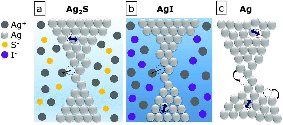 | ||
| Fig. 1 Schematic illustration of the possible sources of resistance fluctuations in Ag nanofilaments: surface fluctuations due to redox exchange of Ag+ ions with the solid electrolyte in Ag2S (a) and in AgI (b) as well as the rearrangement or diffusion of atoms at the surface of stand-alone Ag nanowires (c). As an additional possibility, internal fluctuations between metastable atomic positions within the nanofilament are also indicated in (a–c). | ||
We studied memristive nanojunctions created between a mechanically sharpened PtIr tip of a custom designed scanning tunneling microscope (STM) and Ag/Ag2S thin films. The latter were fabricated by the electron-beam evaporation of an 80 nm thick Ag layer onto a Si substrate followed by a 5-minute long sulfurisation carried out at 60 °C and 5 × 10⁻⁶ mbar resulting in a 30 nm thick stoichiometric Ag2S layer on top of the Ag electrode.55 The analysis of filamentary resistive switching behavior observed in the metallic regime in such Ag/Ag2S/PtIr nanojunctions is reported in ref. 32–35.
Nanometer scale junctions were established at room temperature by the current controlled, low-bias (100 mV) approaching of the PtIr tip to the thin film sample until a direct contact was achieved at a preset, pristine device resistance value of typically a few kΩ. This step was directly followed by current–voltage [I(V)] measurements without the application of a dedicated electroforming procedure. The first few periods were dominated by unstable, non-switching traces before stable resistive switching was acquired. We attribute the former to the initialization of the metallic filament. The necessary electroforming voltage scales down to the range of the set voltage due to the reduced effective thickness of the dielectric layer as the tip is indented to the surface. Resistive switching was verified via the acquisition of hysteretic I(V) characteristics by using the DC setup shown in the inset of Fig. 2(b). A 2.5 Hz triangular Vdrive driving voltage signal was applied to the memristive junction and a series resistor with corresponding resistances of RM and RS, respectively. Typical values of RS were chosen within the 50–1050 Ω interval. The current was monitored using a current amplifier whereas the Vbias voltage drop on the memristor was determined numerically as Vbias = Vdrive − I·RS.
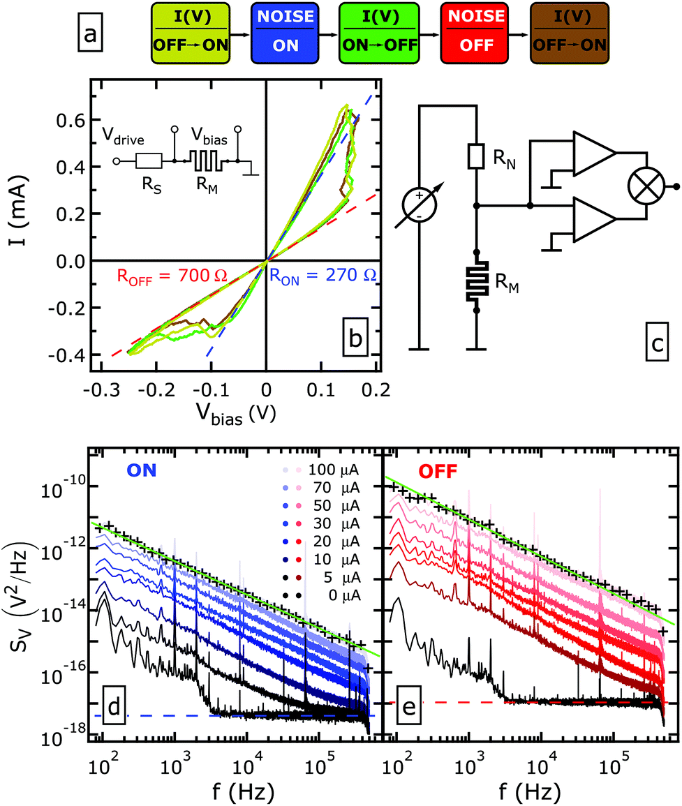 | ||
| Fig. 2 (a) The schematic of subsequent I(V) and noise measurements. (b) Representative hysteretic I(V) characteristics recorded on an Ag/Ag2S/PtIr nanojunction by the application of a triangular Vdrive voltage signal. The colors of the individual traces correspond to those used in (a). The red and blue dashed lines display the OFF and ON state resistances, respectively (ROFF = 700 Ω, RON = 270 Ω), as deduced from the thermal noise floor. The inset shows the circuit diagram of the I(V) measurement setup involving the memristive nanojunction RM and a series resistor RS. (c) The circuit diagram of the noise acquisition setup relying on two parallel low-noise voltage amplifiers and a digitizer board performing the cross-correlation analysis. (d) Noise power density spectra measured in the ON state of the nanojunction recorded at various DC driving currents from 0 to 100 μA. The black crosses and the green line over the 100 μA trace show logarithmically re-sampled data points and their linear fitting, respectively. The blue dashed line is a fit to the thermal noise floor. (e) Identically measured and processed data as in (d) corresponding to the OFF state of the junction. RN = 100 kΩ for all noise measurements. | ||
Once stable resistive switching operation had been confirmed, a remote controlled relay box connected the junction to the dedicated noise measurement setup schematically shown in Fig. 2(c). Here a DC voltage was applied across RN in order to facilitate constant current biasing of the nanojunction. The voltage noise of the junction was amplified by two parallel, battery powered LI-75A low-noise voltage amplifiers and the SV noise power density was acquired using an NI PCI-5922 digitizer in the 100 Hz–500 kHz frequency window at a 1 MHz sampling rate and 22 bit resolution. The internal noise of the amplifiers was eliminated by utilizing the cross-correlation measurement technique.56 In order to further minimize external pick-ups the setup was placed inside a Faraday cage.
The schematic of the subsequent I(V) and noise measurements is illustrated in Fig. 2(a). At first, stable resistive switching was established (yellow line in Fig. 2(b)) which left the junction in its ON state. This was followed by noise measurements as a function of the current bias ranging from 0 to 100 μA (Fig. 2(d)). The upper current limit guarantees that all measurements are carried out within the linear response regime of the nanojunction where resistive switchings do not occur. Consequently, the second I(V) trace (green line in Fig. 2(b)), leaving the junction in its OFF state, overlaps with the previous data. Bias dependent noise spectra are similarly recorded in the OFF state (Fig. 2(e)) and, finally, the acquisition of a third I(V) curve (brown line in Fig. 2(b)) completes the measurements. The data presented in Fig. 2 were verified by two means: (i) the reproducibility of the resistive switchings throughout the entire measurement protocol as demonstrated in Fig. 2(b) and (ii) the quantitative equivalence between the RON and ROFF ON and OFF state resistances determined from the zero-bias slopes of the I(V) traces and from the SV = 4kBTRM thermal noise floor indicated by the blue and red dashed lines in Fig. 2(b, d and e). These criteria, which guarantee that no significant mechanical or electronic drift occurred during the measurement, are routinely satisfied. The observed linearity of the low-bias I(V) characteristics as well as the actual RON = 270 Ω and ROFF = 700 Ω resistance values indicated in Fig. 2(b) are in agreement with our earlier studies on Ag2S based nanojunctions where resistive switching between metallic ON and OFF states was demonstrated to arise from the electric field induced diameter change in highly transparent, continuous metallic nanofilaments.33
Fig. 2(d and e) illustrate that as the current bias is increased up to 100 μA, a significant 1/f type noise emerges in both states of the junction. This dominant contribution is further analyzed by subtracting the bias independent noise floor. Note that the latter significantly deviates from the frequency independent thermal noise below a few kHz. This is partly attributed to the internal noise of the digitizer unit and partly to noise pickups from the environment. However, the resulting low-frequency distortion of the zero bias spectrum is ∼1 (4) orders of magnitude smaller than the noise data acquired at 5 μA (100 μA) current bias in the same frequency regime. The individual spectra were re-sampled to get equidistant data points at the logarithmic frequency scale (8 points per decade) as indicated by the black ‘+’ symbols. The re-sampled traces were fitted against the formula
| SV = β·(f/f0)γ, | (1) |
The dependence of γ and β on the mean current bias as deduced from the data presented in Fig. 2(d and e) is shown in Fig. 3(a) and (b) for the ON and OFF states, respectively. The exponent is γ = −1.17 ± 0.07 in both states. The β values increase with the driving current, as expected for the 1/f type noise.45 As the 1/f type noise usually arises from resistance fluctuations which are present even at zero driving, it can be characterized from its resistance noise power SR = 〈(ΔR)2〉/Δf, i.e. the mean squared deviation of the resistance within a small Δf bandwidth normalized to the bandwidth. Experimentally, however, rather a voltage noise is conveniently measured which scales with the square of the driving current according to Ohm's law (ΔV = I·ΔR) as SV = I2〈(ΔR)2〉/Δf. Consequently, the β values displayed in Fig. 3(a and b) clearly follow an SV ∝ I2 tendency as highlighted by the black dotted lines with a slope of 2 in the log–log plot. This squared current dependence also confirms that the resistance fluctuations reflected in the measured 1/f type noise spectra are not excited by the driving current. We note that the latter statement is only valid for the steady state noise investigated in our experiments, whereas the emergence of additional, driving current induced resistance fluctuations is anticipated close to the resistive switching thresholds.
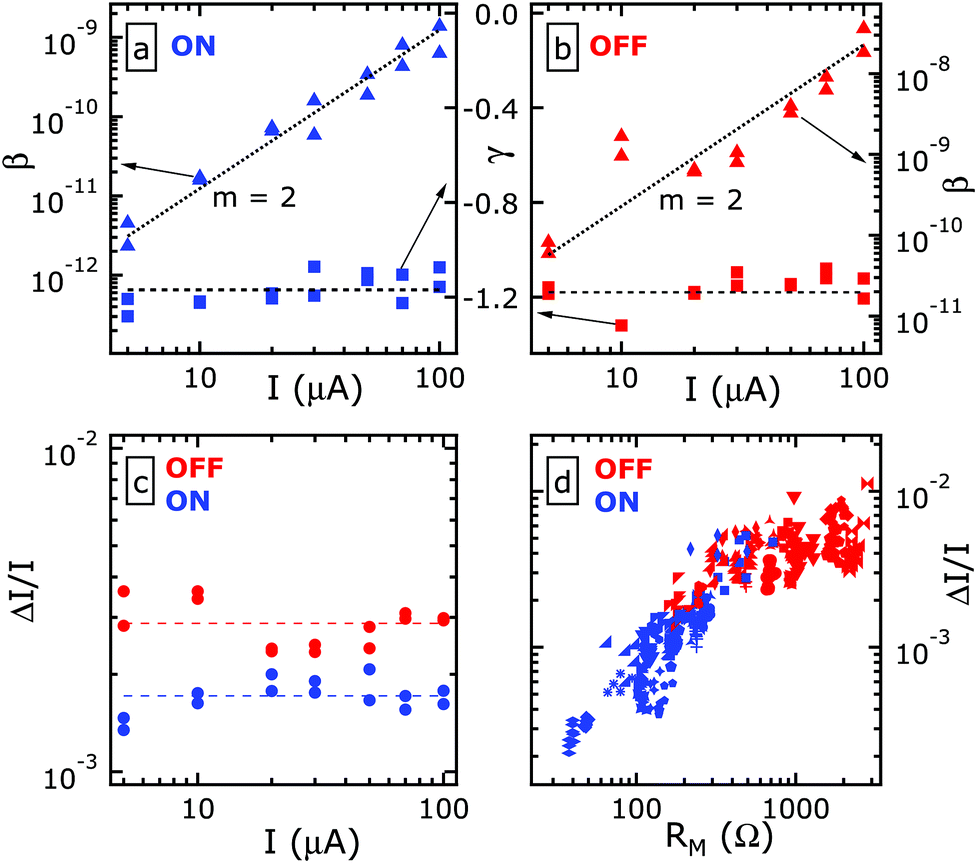 | ||
Fig. 3 (a) Analysis of the ON state noise power density spectra shown in Fig. 2(d). The fitted β coefficients and the γ exponents of eqn (1) are displayed for each driving current by the solid triangles and squares corresponding to the left and right axes, respectively. The dotted line is the best linear fit to the lg β(lg![[thin space (1/6-em)]](https://www.rsc.org/images/entities/char_2009.gif) I) values obtained at a fixed slope of 2. The average of the γ(lgI) values is represented by the dashed line. (b) Similar analysis performed on the OFF state data shown in Fig. 2(e). (c) The current noise ratio as a function of the driving current deduced from the OFF and ON state spectra shown in Fig. 2(d) (red dots) and Fig. 2(e) (blue dots), respectively. The red (blue) dashed line shows the mean value of the OFF (ON) state current noise ratios. (d) Statistical analysis of the current noise ratio measured in an ensemble of independent Ag/Ag2S/PtIr nanojunctions. Identical symbols denote data corresponding to individual devices, and the red (blue) color encodes OFF (ON) states. The resistance was determined from the thermal noise floor of each spectrum. RN = 100 kΩ for all noise measurements. I) values obtained at a fixed slope of 2. The average of the γ(lgI) values is represented by the dashed line. (b) Similar analysis performed on the OFF state data shown in Fig. 2(e). (c) The current noise ratio as a function of the driving current deduced from the OFF and ON state spectra shown in Fig. 2(d) (red dots) and Fig. 2(e) (blue dots), respectively. The red (blue) dashed line shows the mean value of the OFF (ON) state current noise ratios. (d) Statistical analysis of the current noise ratio measured in an ensemble of independent Ag/Ag2S/PtIr nanojunctions. Identical symbols denote data corresponding to individual devices, and the red (blue) color encodes OFF (ON) states. The resistance was determined from the thermal noise floor of each spectrum. RN = 100 kΩ for all noise measurements. | ||
A comparison of Fig. 3(a and b) also evidences that the magnitude of the 1/f type noise is significantly larger in the OFF than that in the ON state. In order to obtain a technologically relevant measurement of the low-frequency noise, we evaluated the current noise ratio (CNR, ΔI/I), i.e. the integrated current fluctuations relative to the mean current calculated as
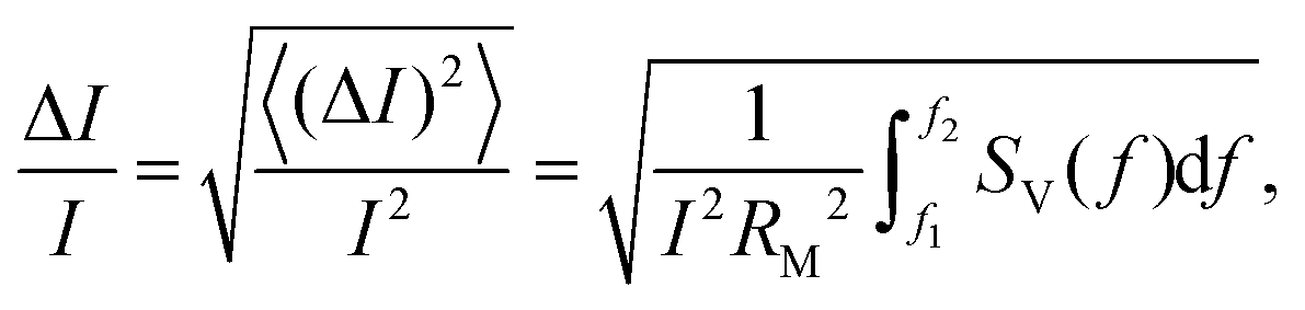 | (2) |
Fig. 3(c) exemplifies that the CNR has a constant value of 0.0017 ± 0.0002 and 0.0029 ± 0.0004 in the ON and OFF states, respectively, as the current is increased. This factor of 1.7 difference between the CNR of the two states was further studied by measuring various resistive switching Ag2S nanojunctions exhibiting a wider range of RON and ROFF resistances. The CNR values corresponding to their ON (OFF) state are displayed in blue (red) in Fig. 3(d) as a function of the resistance whereas the different symbols denote individual devices. The overlapping regime of the red and blue symbols in Fig. 3(d) clearly demonstrates that the CNR solely depends on the device resistance regardless of the ON/OFF nature of the actual device states, that is, different junctions exhibiting the same resistance values in their different states share a common, universal noise level.
In order to explore this universal behavior in more detail we compare the results discussed so far with those obtained on three further nanometer scale systems relying on similar metallic Ag nanojunctions embedded in different microscopic environments. (i) STM based Ag/AgI/PtIr resistive switching nanojunctions57,58 were created in the same manner as the sibling Ag/Ag2S/PtIr structures. The photosensitive AgI thin films were formed directly before the measurements on identical substrate structures by exposing the latter to iodine vapor at 40 °C and ambient pressure for 30 seconds in a dark chamber following the method of Kumar et al.59 Noise measurements were also carried out on atomic scale Ag nanojunctions lacking any resistive switching media by utilizing either (ii) notched Ag wires and the mechanically controllable break-junction (MCBJ) technique60 or (iii) lithographically designed Ag nanobridges and current controlled electromigration.61 The initial structure of the latter method consisted of two-terminal Ag constrictions of 100 nm width, 400–1000 nm length and 40 nm thickness evaporated onto standard, non-switching SiNx substrates.62 The controlled narrowing of the Ag nanobridges was facilitated by sequences of 100 μs long voltage pulses of gradually increasing amplitude with a real-time monitoring of the device current during, and the low-bias resistance between the subsequent pulses.61
Noise measurements and data analysis of the above systems were performed following the procedures described in terms of Fig. 2 and 3. Fig. 4(a) summarizes the complete set of γ exponents deduced from the individual 1/f type spectrum of each investigated device as a function of their resistance. The data set reveals that the various Ag nanojunctions created by four different methods and spanning over three orders of magnitude in resistance are well characterized by the single value of γ = −1.12 ± 0.12. Moreover, Fig. 4(b) demonstrates that the universal resistance dependence of the CNR shown in Fig. 3(d) is not a unique property of metallic Ag/Ag2S/PtIr nanojunctions but a quantitatively reproducible, generic feature of all the four types of the investigated filamentary Ag nanodevices. Surface fluctuations illustrated in Fig. 1 are expected to be predominantly affected by the different microscopic environments of the Ag nanowires in the studied systems. On the other hand, internal resistance fluctuations are determined solely by the bulk defect structure of the Ag filaments, independent of their surroundings. Therefore the observed universality of the CNR indicates that the leading contribution to the 1/f type noise in Ag nanofilaments arises from internal rather than surface induced resistance fluctuations, in accordance with the schematics shown in Fig. 1.
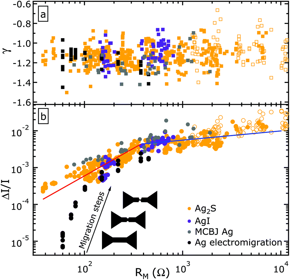 | ||
Fig. 4 (a) The γ exponent of the individual noise spectra as a function of the mean resistance evaluated for a statistical ensemble of independent Ag nanofilaments created in STM based Ag2S (yellow) and AgI (purple) memristive nanojunctions as well as in pure Ag MCBJs (grey) and electromigrated Ag nanobridges (black). The solid yellow, purple and grey (open yellow) symbols correspond to RN = 100 kΩ (RN = 1 MΩ). The solid black data points were recorded with RN = 4.7–12.9 kΩ. (b) The corresponding current noise ratio values as a function of the mean resistance. The blue and red lines represent the best fit to the Ag2S data obtained at fixed exponents of 0.25 and 1.5 corresponding to the ballistic and diffusive conductance regimes in accordance with eqn (3) and (4), respectively. The crossover occurs at around Rcross = 378 Ω. The numerical procedure used l and 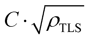 as fitting parameters. The inset illustrates the formation and narrowing of the evaporated Ag nanobridge upon subsequent electromigration steps giving rise to a gradually enhanced current noise ratio. as fitting parameters. The inset illustrates the formation and narrowing of the evaporated Ag nanobridge upon subsequent electromigration steps giving rise to a gradually enhanced current noise ratio. | ||
The actual resistance dependence follows a polynomial tendency; however, around the order of a few hundred Ω a crossover between two different exponents is apparent, as highlighted by the red and blue lines in Fig. 4(b). The low-resistance deviation of the CNR in the evaporated Ag nanobridges with respect to the general trend of the electrochemically and/or mechanically formed junctions highlights the essential differences between the two systems: in the uniform geometry of the former each fluctuator contributes to the total noise with an equally low weight, whereas in the latter arrangement only those scatterers have a high perturbing effect on the conductance which are located in the vicinity of the junction area. Additionally, the formation process of the nanojunctions also introduces a large number of dynamical defects compared to those created during the slow vacuum evaporation of Ag thin films. As the central part of the nanobridge narrows down along the subsequent electromigration steps, this magnified effect of single, nearby fluctuators and of the increased atomic disorder enhances the noise level to the regime of the other structures. It is to be emphasized though, that the magnitude of the CNR remains below the technologically favorable level of ∼1% in all device types throughout the investigated 101–104 Ω resistance interval, i.e. within the entire regime of metallic conductance.
In the following, we outline a theoretical framework based on our earlier work.44 We aim to account for the observed orders of magnitude and resistance dependence of the CNR by taking into account the electron scattering on dynamical defects in point contacts. We consider the ballistic and diffusive conductance regimes, i.e. junctions with diameters smaller or larger than the l mean free path of the electrons, as illustrated in Fig. 5(a) and (b), respectively.
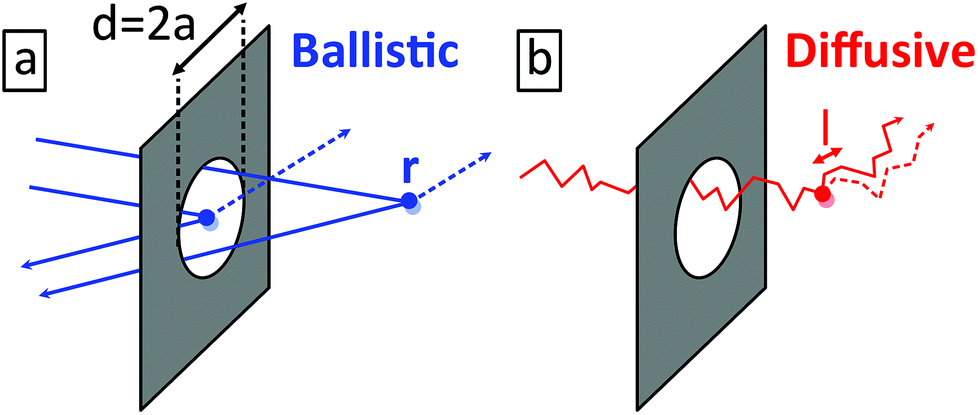 | ||
| Fig. 5 Schematic illustration of electron scattering on dynamical defects in an orifice-like point contact in the ballistic (a) and diffusive (b) conductance regimes. | ||
In the ballistic limit the conductance of an orifice-like point-contact is given by the Sharvin formula, Gball = G0kF2a2/4, where a is the contact radius, kF is the Fermi wavenumber and G0 = 2e2/h ≈ (12.9 kΩ)−1 is the conductance quantum. When an electron is scattered on a dynamical defect close to the junction, Gball is perturbed according to the actual state of the defect resulting in a conductance noise. For the sake of simplicity, the dynamical defects are modeled here as two-level systems (TLSs). We note, however, that the following arguments do not rely on the specific number of available defect states. We model the conductance noise as ΔGball = G0CKball(r), where C quantifies the standard deviation of the temporal conductance fluctuation within the bandwidth of the measurement for a hypothetical TLS positioned in the center of a ballistic contact. The coefficient Kball(r) = Ω2(r)/(2π)2 accounts for the variation of ΔG with the actual position of the TLS where Ω(r) is the solid angle at which the contact is seen from the TLS. We argue that only those processes perturb the conductance where an electron passing through the contact arrives at the given TLS followed by a backscattering through the contact. Consequently, the corresponding probability scales with Ω2(r).44,50 The effect of multiple TLSs is accounted for by assuming a constant ρTLS TLS density and a uniform C for all TLSs. Considering independent TLSs, (ΔG)2 is additive, and is easily integrated over space yielding (ΔG)ball2 = G02C2a3ρTLSIΩ/(2π)4. The 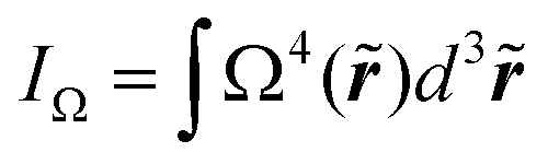 integral with
 ![[r with combining tilde]](https://www.rsc.org/images/entities/b_i_char_0072_0303.gif) = r/a is a constant which is numerically evaluated using the near and far field Taylor series expansion of Ω(r).63 Normalizing ΔGball by Gball the following CNR is obtained:
= r/a is a constant which is numerically evaluated using the near and far field Taylor series expansion of Ω(r).63 Normalizing ΔGball by Gball the following CNR is obtained:
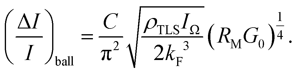 | (3) |
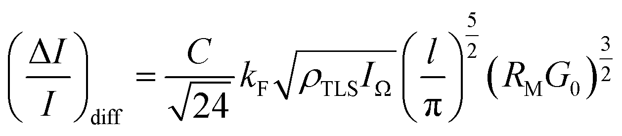
In a diffusive junction the Sharvin formula is replaced by the Maxwell conductance Gdiff = 2aσ = Gball8l/(3πa), where σ is the conductivity; see eqn (36) in ref. 44. According to eqn (167) of ref. 44, due to the diffusive environment of the TLS, the geometrical coefficient is reduced as Kdiff(r) = Kball(r)·(l/a)2. As a result,
 | (4) |
These considerations predict slopes of 3/2 and 1/4 for the RM dependent CNR data on the log–log scale. We fit the above model to our Ag2S CNR data by determining the Rcross resistance where eqn (3) and (4) intersect, and using the ballistic (diffusive) CNR formula at RM > Rcross (RM < Rcross). The least squares fitting performed on the log–log scale is illustrated in Fig. 4(b) with a blue (red) line in the ballistic (diffusive) segment. Using the numerical value64 of kF = 12 nm−1 the fitting yields l = 1 ± 0.14 nm and 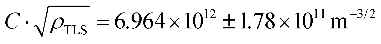 . The RM dependence of the CNR predicted by this simple model clearly follows the experimentally observed tendencies both in the ballistic and diffusive regimes. The resulting mean free path of l = 1 nm is smaller than the 4 ± 1 nm obtained from conductance fluctuation measurements carried out at cryogenic temperatures,65 which we attribute to the enhanced scattering on phonons and dynamical defects at room temperature. The diameter of a junction at the diffusive-ballistic crossover can be estimated by substituting the values of Rcross and kF into the Sharvin formula or, more accurately, into the Wexler formula.66 The resulting d = 2a = 1.95 nm (Sharvin) or d = 1.56 nm (Wexler) is indeed in the range of the mean free path, as expected at the crossover. In ref. 50 two-level fluctuations with ΔG ≈ 0.5G0 were both experimentally observed and theoretically estimated for a single TLS located in the contact region. Using the corresponding value of C = 0.5 we can estimate the average distance between neighboring TLSs as lTLS = (ρTLS)−1/3 = 1.7 nm which is close to the estimated mean free path value.
Although the above numerical values are rough estimates, their magnitudes clearly indicate that close-to-atomic-sized Ag nanowires established by electrochemical metallization, mechanical rupture or electromigration techniques exhibit a large degree of disorder and a number of dynamical defects in the junction region resulting in a much shorter mean free path than that in thin film samples. Based on the measured resistivity of our as-deposited Ag nanobridges, the latter was evaluated to be ≈16.5 nm. The above numerical estimates confirm our argument that the enhanced dynamical defect density in the junction region together with the magnifying effect of the point contact geometry lead to the almost two orders of magnitude larger CNR in a point contact device than that in an as-deposited nanobridge device displaying the same resistance.
In conclusion, we have studied the 1/f type noise in STM based Ag/Ag2S/PtIr and Ag/AgI/PtIr resistive switching nanojunctions as well as in pure Ag nanowires created by MCBJ and controlled electromigration techniques. Our comparative analysis indicates that the noise contribution arising from the internal resistance fluctuations of the various Ag nanofilaments dominates over the effect of environmental perturbations. We found that as long as resistive switching takes place between metallic states exhibiting continuous Ag filaments, the total noise solely and universally depends on the device resistance. This dependence is quantitatively captured with a theoretical model taking electron scattering in dynamical defects into account. By revealing the diffusive to ballistic crossover, this model also provided a numerical estimate on the defect density in electrochemically or mechanically created Ag nanowires. Our study points out that in spite of the deduced, relatively high defect density, the total current noise remains at a technologically convenient level of a few percent of the mean current even in ballistic, truly nanometer scale resistive switching junctions, demonstrating the merits of the latter as a viable hardware platform for novel neuromorphic architectures.
Conflicts of interest
There are no conflicts to declare.Acknowledgements
This work was supported by the BME-Nanonotechnology FIKP grant of EMMI (BME FIKP-NAT) and the NKFI K119797 and K128534 grants. B. S. acknowledges the support of the UNKP-18-3 New National Excellence Program of the Ministry of Human Capacities. In grateful memory of Alfred Zawadowski.References
- L. Chua, IEEE Trans. Circuit Theory, 1971, 18, 507–519 Search PubMed.
- D. B. Strukov, G. S. Snider, D. R. Stewart and R. S. Williams, Nature, 2008, 453, 80–83 CrossRef CAS PubMed.
- J. J. Yang, D. B. Strukov and D. R. Stewart, Nat. Nanotechnol., 2013, 8, 13–24 CrossRef CAS PubMed.
- M. A. Zidan, J. P. Strachan and W. D. Lu, Nat. Electron., 2018, 1, 22–29 CrossRef.
- A. Chung, J. Deen, J.-S. Lee and M. Meyyappan, Nanotechnology, 2010, 21, 412001 CrossRef PubMed.
- G. H. Kim, J. H. Lee, Y. Ahn, W. Jeon, S. J. Song, J. Y. Seok, J. H. Yoon, K. J. Yoon, T. J. Park and C. S. Hwang, Adv. Funct. Mater., 2013, 23, 1440–1449 CrossRef CAS.
- S. H. Jo, T. Kumar, S. Narayanan and H. Nazarian, IEEE Trans. Electron Devices, 2015, 62, 3477–3481 Search PubMed.
- S. Ambrogio, P. Narayanan, H. Tsai, R. M. Shelby, I. Boybat, C. di Nolfo, S. Sidler, M. Giordano, M. Bodini, N. C. P. Farinha, B. Killeen, C. Cheng, Y. Jaoudi and G. W. Burr, Nature, 2018, 558, 60 CrossRef CAS PubMed.
- G. W. Burr, R. M. Shelby, A. Sebastian, S. Kim, S. Kim, S. Sidler, K. Virwani, M. Ishii, P. Narayanan, A. Fumarola, L. L. Sanches, I. Boybat, M. L. Gallo, K. Moon, J. Woo, H. Hwang and Y. Leblebici, Adv. Phys.: X, 2017, 2, 89–124 Search PubMed.
- K. Terabe, T. Hasegawa, T. Nakayama and M. Aono, Nature, 2005, 433, 47–50 CrossRef CAS PubMed.
- J. J. T. Wagenaar, M. Morales-Masis and J. M. van Ruitenbeek, J. Appl. Phys., 2012, 111, 014302 CrossRef.
- G. Indiveri, B. Linares-Barranco, R. Legenstein, G. Deligeorgis and T. Prodromakis, Nanotechnology, 2013, 24, 384010 CrossRef PubMed.
- G. Indiveri and S.-C. Liu, Proc. IEEE, 2015, 103, 1379–1397 CAS.
- Z. Wang, S. Joshi, S. E. Savelev, H. Jiang, R. Midya, P. Lin, M. Hu, N. Ge, J. P. Strachan, Z. Li, Q. Wu, M. Barnell, G.-L. Li, H. L. Xin, R. S. Williams, Q. Xia and J. J. Yang, Nat. Mater., 2016, 16, 101–108 CrossRef PubMed.
- L. Appeltant, M. C. Soriano, G. V. der Sande, J. Danckaert, S. Massar, J. Dambre, B. Schrauwen, C. R. Mirasso and I. Fischer, Nat. Commun., 2011, 2, 468 CrossRef CAS PubMed.
- A. V. Avizienis, H. O. Sillin, C. Martin-Olmos, H. H. Shieh, M. Aono, A. Z. Stieg and J. K. Gimzewski, PLoS One, 2012, 7, e42772 CrossRef CAS PubMed.
- H. O. Sillin, R. Aguilera, H.-H. Shieh, A. V. Avizienis, M. Aono, A. Z. Stieg and J. K. Gimzewski, Nanotechnology, 2013, 24, 384004 CrossRef PubMed.
- K. S. Scharnhorst, J. P. Carbajal, R. C. Aguilera, E. J. Sandouk, M. Aono, A. Z. Stieg and J. K. Gimzewski, Jpn. J. Appl. Phys., 2018, 57, 03ED02 CrossRef.
- F. Alibart, E. Zamanidoost and D. B. Strukov, Nat. Commun., 2013, 4, 2072 CrossRef PubMed.
- A. A. Balandin, Nat. Nanotechnol., 2013, 8, 549–555 CrossRef CAS PubMed.
- P. Puczkarski, Q. Wu, H. Sadeghi, S. Hou, A. Karimi, Y. Sheng, J. H. Warner, C. J. Lambert, G. A. D. Briggs and J. A. Mol, ACS Nano, 2018, 12, 9451–9460 CrossRef CAS PubMed.
- S. Tewari and J. van Ruitenbeek, Nano Lett., 2018, 18, 5217–5223 CrossRef CAS PubMed.
- K. Terabe, T. Nakayama, T. Hasegawa and M. Aono, Appl. Phys. Lett., 2002, 80, 4009–4011 CrossRef CAS.
- S. H. Jo and W. Lu, Nano Lett., 2008, 8, 392–397 CrossRef CAS PubMed.
- S. H. Jo, K.-H. Kim and W. Lu, Nano Lett., 2009, 9, 870–874 CrossRef CAS PubMed.
- S. H. Jo, T. Chang, I. Ebong, B. B. Bhadviya, P. Mazumder and W. Lu, Nano Lett., 2010, 10, 1297–1301 CrossRef CAS PubMed.
- H. Sun, Q. Liu, C. Li, S. Long, H. Lv, C. Bi, Z. Huo, L. Li and M. Liu, Adv. Funct. Mater., 2014, 24, 5679–5686 CrossRef CAS.
- A. Nayak, T. Tamura, T. Tsuruoka, K. Terabe, S. Hosaka, T. Hasegawa and M. Aono, J. Phys. Chem. Lett., 2010, 1, 604–608 CrossRef CAS.
- I. Valov, I. Sapezanskaia, A. Nayak, T. Tsuruoka, T. Bredow, T. Hasegawa, G. Staikov, M. Aono and R. Waser, Nat. Mater., 2012, 11, 530–535 CrossRef CAS PubMed.
- Y. Yang, P. Gao, S. Gaba, T. Chang, X. Pan and W. Lu, Nat. Commun., 2012, 3, 732 CrossRef PubMed.
- Y. Yang, P. Gao, L. Li, X. Pan, S. Tappertzhofen, S. Choi, R. Waser, I. Valov and W. D. Lu, Nat. Commun., 2014, 5, 4232 CrossRef CAS PubMed.
- A. Geresdi, A. Halbritter, A. Gyenis, P. Makk and G. Mihály, Nanoscale, 2011, 3, 1504–1507 RSC.
- A. Geresdi, M. Csontos, A. Gubicza, A. Halbritter and G. Mihály, Nanoscale, 2014, 6, 2613 RSC.
- A. Gubicza, M. Csontos, A. Halbritter and G. Mihály, Nanoscale, 2015, 7, 4394–4399 RSC.
- A. Gubicza, M. Csontos, A. Halbritter and G. Mihály, Nanoscale, 2015, 7, 11248–11254 RSC.
- S. Wu, T. Tsuruoka, K. Terabe, T. Hasegawa, J. P. Hill, K. Ariga and M. Aono, Adv. Funct. Mater., 2011, 21, 93–99 CrossRef CAS.
- S. R. Mohapatra, T. Tsuruoka, K. Krishnan, T. Hasegawa and M. Aono, J. Mater. Chem. C, 2015, 3, 5715–5720 RSC.
- W. Chen, S. Tappertzhofen, H. J. Barnaby and M. N. Kozicki, J. Electroceram., 2017, 39, 109–131 CrossRef CAS.
- S. Choi, S. H. Tan, Z. Li, Y. Kim, C. Choi, P.-Y. Chen, H. Yeon, S. Yu and J. Kim, Nat. Mater., 2018, 17, 335–340 CrossRef CAS PubMed.
- R. Waser, R. Dittmann, G. Staikov and K. Szot, Adv. Mater., 2009, 21, 2632–2663 CrossRef CAS.
- M. Morales-Masis, S. J. van der Molen, T. Hasegawa and J. M. van Ruitenbeek, Phys. Rev. B: Condens. Matter Mater. Phys., 2011, 84, 115310 CrossRef.
- D. Ielmini, F. Nardi and C. Cagli, Appl. Phys. Lett., 2010, 96, 053503 CrossRef.
- Y. Li, K.-S. Yin, M.-Y. Zhang, L. Cheng, K. Lu, S.-B. Long, Y. Zhou, Z. Wang, K.-H. Xue, M. Liu and X.-S. Miao, Appl. Phys. Lett., 2017, 111, 213505 CrossRef.
- A. Halbritter, L. Borda and A. Zawadowski, Adv. Phys., 2004, 53, 939–1010 CrossRef CAS.
- S. Kogan, Electronic noise and fluctuations in solids, Cambridge University Press, New York, 1996 Search PubMed.
- P. Dutta and P. M. Horn, Rev. Mod. Phys., 1981, 53, 497–516 CrossRef CAS.
- F. N. Hooge, T. G. M. Kleinpenning and L. K. J. Vandamme, Rep. Prog. Phys., 1981, 44, 479–532 CrossRef.
- M. B. Weissman, Rev. Mod. Phys., 1988, 60, 537–571 CrossRef CAS.
- M. J. Kirton and M. J. Uren, Adv. Phys., 1989, 38, 367–468 CrossRef CAS.
- P. A. M. Holweg, J. Caro, A. H. Verbruggen and S. Radelaar, Phys. Rev. B: Condens. Matter Mater. Phys., 1992, 45, 9311–9319 CrossRef.
- A. Bid, A. Bora and A. K. Raychaudhuri, Nanotechnology, 2006, 17, 152–156 CrossRef.
- M.-S. Lee, J.-K. Lee, H.-S. Hwang, H.-C. Shin, B.-G. Park, Y.-J. Park and J.-H. Lee, Jpn. J. Appl. Phys., 2011, 50, 011501 CrossRef.
- S. Agarwal, S. J. Plimpton, D. R. Hughart, A. H. Hsia, I. Richter, J. A. Cox, C. D. James and M. J. Marinella, 2016 Int. Jt. Conf. Neural Networks, 2016, 929–938 Search PubMed.
- N. Gong, T. Idé, S. Kim, I. Boybat, A. Sebastian, V. Narayanan and T. Ando, Nat. Commun., 2018, 9, 2102 CrossRef CAS PubMed.
- A. Geresdi, A. Halbritter, E. Szilágyi and G. Mihály, MRS Proc., 2011, 1331 DOI:10.1557/opl.2011.1474.
- H. E. van den Brom and J. M. van Ruitenbeek, Phys. Rev. Lett., 1999, 82, 1526–1529 CrossRef CAS.
- X. F. Liang, Y. Chen, L. Shi, J. Lin, J. Yin and Z. G. Liu, J. Phys. D: Appl. Phys., 2007, 40, 4767–4770 CrossRef CAS.
- H. X. Guo, B. Yang, L. Chen, Y. D. Xia, K. B. Yin, Z. G. Liu and J. Yin, Appl. Phys. Lett., 2007, 91, 243513 CrossRef.
- P. S. Kumar and C. S. Sunandana, Thin Solid Films, 1998, 323, 110–114 CrossRef.
- Z. Balogh, D. Visontai, P. Makk, K. Gillemot, L. Oroszlány, L. Pósa, C. Lambert and A. Halbritter, Nanoscale, 2014, 6, 14784–14791 RSC.
- A. Gubicza, D. Z. Manrique, L. Pósa, C. J. Lambert, G. Mihály, M. Csontos and A. Halbritter, Sci. Rep., 2016, 6, 30775 CrossRef CAS PubMed.
- E. Tóvari, M. Csontos, T. Kriváchy, P. Fürjes and S. Csonka, Appl. Phys. Lett., 2014, 105, 123114 CrossRef.
- I. S. Jones, Int. J. Math. Educ. Sci. Technol., 1996, 27, 667–674 CrossRef.
- C. Kittel, Introduction to Solid State Physics, John Wiley & Sons, Inc, 8th edn, 2005 Search PubMed.
- B. Ludoph and J. M. van Ruitenbeek, Phys. Rev. B: Condens. Matter Mater. Phys., 2000, 61, 2273–2285 CrossRef CAS.
- A. Wexler, Proc. Phys. Soc., 1966, 89, 927 CrossRef.
Footnote |
| † These authors contributed equally to this work. |
| This journal is © The Royal Society of Chemistry 2019 |