
 Open Access Article
 This Open Access Article is licensed under a
 Creative Commons Attribution 3.0 Unported Licence
The role of excitons within the hole transporting layer in quantum dot light emitting device degradation†
Tyler
Davidson-Hall
 * and
Hany
Aziz
* and
Hany
Aziz
Department of Electrical and Computer Engineering and Waterloo Institute for Nanotechnology, University of Waterloo, 200 University Avenue West, Waterloo, Ontario N2L 3G1, Canada. E-mail: tadavids@uwaterloo.ca
First published on 15th April 2019
Abstract
This work investigates the root causes of the limited stability of electroluminescent quantum dot light-emitting devices (QDLEDs). Studies using electrical measurements, continuous UV irradiation, and both steady-state and transient photoluminescence (PL) spectroscopy reveal that exciton-induced degradation of the hole transporting material (HTM) in QDLEDs plays a role in limiting their electroluminescence (EL) stability. The results indicate that there is a correlation between device EL stability and the susceptibility of the HTM to exciton-induced degradation. The presence of quenchers in the HTM layer can lead to a decrease in the luminescence quantum yield of QDs, suggesting that energy transfer between the QD and HTM films may play a role in this behavior. The results uncover a new degradation mechanism where excitons within the HTM limit the EL stability of QDLEDs.
1. Introduction
The unique properties of colloidal quantum dots (QDs) such as high photoluminescence (PL) quantum yield approaching 100%, narrow and tunable electroluminescence (EL) spectra, and solution-compatibility for low cost processing make them advantageous for use as an electroluminescent material in light-emitting devices.1–7 Significant progress in developing improved QD materials and device structures, including the use of inorganic (typically ZnO) materials for the electron transport layer and organic materials for the hole transport (HTM) layer, has drastically improved the performance of quantum dot light-emitting devices (QDLEDs) over the last two decades.8–11 Indeed, external quantum efficiency (EQE) and EL lifetime (LT50) as high as 20.5% and 300![[thin space (1/6-em)]](https://www.rsc.org/images/entities/char_2009.gif) 000 hours (for an initial luminance of 100 cd m−2) were reported for CdSe-core QDLEDs, respectively.12,13 Nevertheless, the lifetime of most QDLEDs remains inadequate for commercial applications. In addressing the limited stability of QDLEDs, significant attention has been given to reducing charge imbalance and Auger recombination in the QDs, which ensue from defects in the QDs and the large energy level mismatch between the valence band of the QD core or shell and the Highest Occupied Molecular Orbital (HOMO) energy level of the HTM that makes hole injection into the QDs difficult.12–19 Recently, Chang et al.20 pointed to a possible detrimental effect of electrons on HTMs of QDLEDs. Additional degradation phenomena within QDLEDs have received comparably minor attention.
000 hours (for an initial luminance of 100 cd m−2) were reported for CdSe-core QDLEDs, respectively.12,13 Nevertheless, the lifetime of most QDLEDs remains inadequate for commercial applications. In addressing the limited stability of QDLEDs, significant attention has been given to reducing charge imbalance and Auger recombination in the QDs, which ensue from defects in the QDs and the large energy level mismatch between the valence band of the QD core or shell and the Highest Occupied Molecular Orbital (HOMO) energy level of the HTM that makes hole injection into the QDs difficult.12–19 Recently, Chang et al.20 pointed to a possible detrimental effect of electrons on HTMs of QDLEDs. Additional degradation phenomena within QDLEDs have received comparably minor attention.
We have previously found that excitons are present in the HTM layer under standard operating conditions of QDLEDs. These excitons arise from the drift of electrons past the QD emissive layer and their recombination with holes in the HTM layer.21 Knowing that organic materials are susceptible to damage by excitons, a phenomenon that has been found to have a detrimental effect on the stability of organic layers in light-emitting devices,22–24 the possibility of exciton-induced degradation of the HTM playing a role in the limited electroluminescence stability of QDLEDs must be considered. This notion is particularly compelling once the remarkable stability of the other layers is taken into consideration. QDs have exhibited excellent intrinsic PL stability with recent accelerated aging tests of thick-shelled QD light-converting films retaining 100% of their initial PL intensity after 9000 hours, corresponding to a lifetime of 100000 hours.25 Meanwhile, ZnO and other metal oxides used as transport materials are known to generally have high chemical and electrical robustness.10,11,13,26,27
The objective of this work is to investigate the influence of HTMs on the stability of QDLEDs and to understand the role that excitons play with respect to degradation in these devices. We observe a significant difference in LT50 between QDLEDs that otherwise exhibit equivalent efficiency, charge transport and injection properties. Notably, we find that the PL stability of QDs can change upon changing the HTM (and the latter's susceptibility to damage by excitons), and that a correlation exists between that behavior and the EL stability of the QDLEDs. To the best of our knowledge, this work represents the first investigation into the effect of excitons in the hole transport layers of QDLEDs and their influence on device stability. Although the measurements presented in this work primarily investigate photo-induced excitons, we demonstrate that excitons are similarly formed deep within the HTM layer during electrical bias, indicating that the same phenomena must also occur during normal QDLED operation. The results therefore reveal that the robustness of the HTM to exciton-induced degradation is a critical factor for QDLED stability.
2. Experimental details
Device fabrication
The QDLEDs studied here were fabricated on 100 nm thick ITO patterned glass substrates (Kintec) with 20 Ω sq−1 sheet resistance, cleaned and sonicated sequentially with Micro 90, deionized water, and isopropanol solutions before treating with O2 plasma for 5 minutes. ZnO sol–gel was prepared by adding zinc acetate (197 mg, Sigma-Aldrich) to ethanolamine (54 μL, Sigma-Aldrich) in ethanol (6 mL, Sigma-Aldrich) and mixing at 600 RPM for 40 minutes and a temperature of 45 °C. The ZnO solutions were filtered through a 0.22 μm polypropylene filter, spincoated at a rotational speed of 1000 RPM for 60 seconds, and annealed at 180 °C for 30 minutes. Red CdSe/CdS quantum dot rods suspended in octane with a peak EL emission wavelength of 630 nm (0.6 mg mL−1, Strem Chemicals #48-1059, with >80% quantum yield and size of approximately 5 nm diameter by 20 nm width) were spincoated at a rotational speed of 2000 RPM for 60 seconds, then annealed at 50 °C for 30 minutes. The same deposition process was used for green CdSe/CdS quantum dot rods with a peak EL emission wavelength of 550 nm (0.6 mg mL−1, Strem Chemicals #48-1053, with >60% quantum yield and size of approximately 5 nm diameter by 20 nm width). The organic 4,4′-bis(N-carbazolyl)-1,1′-biphenyl (CBP) (Shanghai Han Feng Chemical Co.), N,N′-di(1-naphthyl)-N,N′-diphenyl-(1,1′-biphenyl)-4,4′-diamine (NPB) (Shanghai Han Feng Chemical Co.), 2,2′,7,7′-tetrakis(carbazol-9-yl)-9,9-spirobifluorene (Spiro-CBP) (Luminescence Technology Corp.), 2,6-bis[3-(9H-carbazol-9-yl)phenyl]pyridine (2,6-DCzPPy) (EM Index), 1,3-bis(N-carbazolyl)benzene (mCP) (Jilin OLED Material Tech Co.), 2,2′,2′′-(1,3,5-benzinetriyl)-tris(1-phenyl-1-H-benzimidazole) (TPBi) (Shanghai Han Feng Chemical Co.), 2-tert-butyl-9,10-di(naphth-2-yl)anthracene (TBADN) (Luminescence Technology Corp.), 4-(dicyanomethylene)-2-t-butyl-6-(1,1,7,7-tetramethyljulolidyl-9-enyl)-4H-pyran (DCJTB) (Shanghai Han Feng Chemical Co.), MoO3 hole injection layer (HIL) (Angstrom Engineering), and aluminum anode (Angstrom Engineering) were deposited at a rate of 0.1–2 Å s−1 in an Angstrom Engineering EvoVac thermal evaporation chamber at a base pressure of 5 × 10⁻⁶ Torr.Device characterization
Luminance of the QDLEDs was measured with a Minolta Chroma Meter CS-100, and current–voltage–luminance measurements were carried out via an Agilent 4155C Semiconductor Parameter Analyzer connected to a silicon photodiode. Spectral measurements of the QDLEDs were measured using an Ocean Optics QE65000 spectrometer. External quantum efficiencies were calculated as described by Okamoto et al. assuming a Lambertian emission distribution.28 Photoluminescence was induced via irradiation with an Analytik Jena UVL-18 handheld ultraviolet lamp with 370 nm peak emission. Transient PL decay was measured with an Edinburgh Instruments FL920 spectrometer equipped with a 375 nm peak emission EPL375 picosecond pulsed laser diode. Electroluminescence lifetime measurements were performed in a Botest Systems GmbH OLT Lifetime Test System with a constant driving current maintained at 20 mA cm−2. During all device tests, aside from transient PL measurements, the QDLEDs were kept in a nitrogen atmosphere.3. Results and discussion
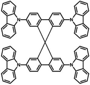
Initial investigations into the role of the hole transporting layer in QDLED stability were carried out by fabricating red-emitting devices with the same structure but different HTMs and comparing their EL performance. The general structure of these devices was: ITO (100 nm)/ZnO (35 nm)/QD (15 nm)/HTM (40 nm)/MoO3 (5 nm)/Al (100 nm). CBP, Spiro-CBP, 2,6-DCzPPy, NPB, and mCP were selected for use as HTMs due to their range of HOMO energy levels. The key performance characteristics of these devices are detailed in Table 1 along with the molecular structure, glass transition temperature, HOMO and band gap energy of each HTM, with source curves available in Fig. S1 of the ESI.† Devices utilizing a mCP HTM are omitted from Table 1 as the QDLEDs were inoperable due to the instability of mCP as a HTM. QDLEDs utilizing CBP as the HTM result in the most efficient devices. The turn-on voltage for the CBP QDLED occurs at a bias roughly coinciding with the 2 eV band gap of a QD with 630 nm luminescence peak emission. Interestingly, the NPB QDLED exhibits a sub-bandgap turn-on voltage which has been attributed to Auger-assisted hole injection.29 However, in this case the efficiency of such devices is much lower than those that do not exhibit sub-bandgap turn-on voltages, likely due to the shallow HOMO energy level of NPB which limits hole injection into the QDs. 2,6-DCzPPy and Spiro-CBP both produce QDLEDs with higher turn-on and driving voltages (at a current density of 20 mA cm−2), compared to CBP QDLEDs. In the case of 2,6-DCzPPy, lower hole mobility and a deeper HOMO energy level may cause the rightward shift in current density–voltage (JV) characteristics. Given the molecular structure and energy level similarity between CBP and Spiro-CBP, the vast difference in QDLED performance is unexpected but appears to be a result of poor hole injection. Furthermore, the CBP QDLED also exhibits a significantly longer lifetime; an order of magnitude greater than the alternatives despite its higher initial luminance. An examination of the HTM's HOMO and glass transition temperature values reveals no clear correlation between these properties and the QDLED stability trends. There is, however, a weak inverse correlation between the band gap energy and the QDLED EL lifetimes where devices utilizing HTMs with larger band gaps demonstrate lower stability. Previous work has identified a correlation between the band gap energy of organic materials and their propensity to undergo exciton–polaron induced aggregation.37 Although these results show that the HTM has a significant influence on QDLED performance, the difference in stability may simply be due to variance in charge balance and/or exciton density in view that the devices have different JV and EQE characteristics.| HTM | Molecular structure | HOMO energy level (eV) | Band gap energy (eV) | Glass transition temperature (°C) | Turn-on voltage (V) | Performance at 20 mA cm−2 driving current density | |||
|---|---|---|---|---|---|---|---|---|---|
| Driving voltage (V) | Luminance (cd m−2) | EQE (%) | LT50 (h) | ||||||
| CBP |

|
−5.9 (ref. 30) | 3.3 (ref. 30) | 62 (ref. 31) | 2.09 | 2.82 | 760 | 3.5 | 13 |
| Spiro-CBP |
|
−5.8 (ref. 32) | 3.4 (ref. 32) | 240 (ref. 33) | 4.17 | 7.68 | 140 | 0.7 | <1 |
| 2,6-DCzPPy |

|
−6.1 (ref. 34) | 3.5 (ref. 34) | 102 (ref. 34) | 2.82 | 5.04 | 340 | 1.5 | <1 |
| NPB |

|
−5.4 (ref. 35) | 3.0 (ref. 35) | 96 (ref. 36) | 1.49 | 2.85 | 60 | 0.3 | N/A |
Therefore, to test the effect of different HTMs on the stability of QDLEDs more accurately and rule out the confounding effects of differences in charge balance and/or exciton density, only devices with comparable JV behavior and efficiency should be compared. The efficiency and transport difference between the CBP and Spiro-CBP appears to arise from an injection issue at the Spiro-CBP/MoO3 interface which can be remedied by introducing a 10 nm interstitial layer of CBP doped with 5% MoO3. By selecting thicknesses of 30 nm for Spiro-CBP and 50 nm for CBP, the JV curves for both QDLED structures essentially coincide and exhibit almost equal turn-on and driving voltage with minimal leakage current as can be seen in Fig. 1. Although the Spiro-CBP device has a slightly higher maximum EQE and more efficiency roll-off at high current density, the two QDLEDs exhibit similar EQE at 20 mA cm−2 driving current density. Given their coinciding characteristics, any differences in stability between these devices will not be primarily due to differences in charge balance or exciton density. Fig. 2 presents the EL stability test results from the CBP and Spiro-CBP devices optimized for matching performance, showing the changes in luminance and driving voltage over time at a driving current density of 20 mA cm−2. The initial luminance of the two devices at this driving current were very similar, with values of 1450 cd m−2 and 1440 cd m−2 for the CBP and Spiro-CBP QDLEDs, respectively. In line with the results covered in Table 1, the device with a CBP HTM once again exhibits a LT50 that is an order of magnitude longer than that of its counterpart with a Spiro-CBP HTM. The CBP QDLED has a remarkably stable driving voltage throughout the testing period whereas the driving voltage of the Spiro-CBP QDLED structure experiences a rapid increase, especially in the first 3 hours. This rapid increase occurs in the same time frame during which the luminance decreased by 80%. These results indicate that QDLEDs incorporating Spiro-CBP are inherently less stable than comparable devices with CBP as the HTM.
 | ||
| Fig. 1 (a) EQE vs. current density, (b) Luminance (dashed) and current density (solid) vs. voltage characteristics for QDLEDs designed for matching performance with CBP (red square) and Spiro-CBP (blue circle) HTMs. | ||
 | ||
| Fig. 2 EL stability test results from the CBP (red square) and Spiro-CBP (blue square) QDLEDs optimized for matching performance, showing the changes in luminance (solid) and driving voltage (ΔV = V(t) − V(0)) (dashed) over time at 20 mA cm−2 driving current density. | ||
Knowing that excitons can damage organic materials to various extents, we investigate whether the differences in QDLED EL stability upon changing the HTM may be due to exciton-induced degradation effects. To this end, we study the effect of subjecting the QDLEDs with various HTMs to UV irradiation continuously, for 80 hours, while monitoring changes in the intensity of the QD and HTM PL spectra, which would mirror changes in their PL quantum yields. QDLEDs with the general device structure of ITO (100 nm)/ZnO (35 nm)/QD (15 nm)/HTM (40 nm)/MoO3 (5 nm)/Al (100 nm), were fabricated and tested, using CBP, Spiro-CBP, 2,6-DCzPPy, NPB, and mCP HTMs. A UV lamp with peak luminescence at a wavelength of 370 nm was used as an excitation source at an irradiation power of 500 μW cm−2. Excitation at this wavelength can induce the formation of excitons in QDs, CBP, Spiro-CBP and NPB (which all have non-negligible absorption at 370 nm), producing PL from both the QDs and the HTM in each case. However, there was no detectable HTM PL emission from 2,6-DCzPPy and mCP devices. One example of the spectral intensity change over time is presented in Fig. 3(a) for the CBP QDLED, while similar figures for the other QDLED structures can be found in the ESI.† The trends in QD and HTM peak PL over the entire 80-hour irradiation period can be found in Fig. 3(b) and (c), respectively. To facilitate visualization of the changes in quantum yield, the changes in peak intensity are normalized to both the initial intensity at t0 and the excitation intensity. As can be seen from the figure, the QD PL intensity of the CBP QDLED exhibits a 16% increase in the first 10 hours and then starts to decrease slowly to 106% of the initial intensity by the 80-hour point. In contrast, the QD PL intensity for the NPB device increases rapidly by 40% over the first 10 hours of irradiation and then reaches a plateau at 145% of the initial PL intensity. There is a minor increase of 7% in QD PL intensity over the first few hours with a Spiro-CBP HTM, which gradually decreases to 75% by the end of the 80-hour measurement period. Meanwhile, the QD PL intensity for devices with a 2,6-DCzPPy HTM undergoes minimal changes over the first 10 hours of UV irradiation and ultimately degrades by 10% after 80 hours. Furthermore, the mCP QDLED exhibits an extreme degradation in QD PL by 35% over the initial 10 hours of UV irradiation which begins to slow toward an emission intensity equivalent to 48% of the initial value by the 80-hour mark. The stark difference between the PL trends of the five QDLEDs indicates that the HTM next to the QD layer has a significant influence on QD luminescence behavior over time.
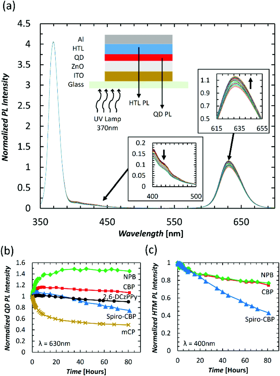 | ||
| Fig. 3 (a) PL spectra of a CBP QDLED over 80 hours of constant UV irradiation with insets indicating the device structure and source of measured PL emission (top), the change in measured CBP PL intensity (bottom), and QD PL intensity (right). (b) QD peak PL intensity vs. time and (c) HTM peak PL intensity vs. time for CBP (red square), NPB (green diamond), Spiro-CBP (blue triangle), 2,6-DCzPPy (black circle), and mCP (gold cross) QDLEDs subjected to constant UV irradiation. The 370 nm band corresponds to the UV excitation peak. 2,6-DCzPPy and mCP HTM bands could not be detected. | ||
Unlike the trends observed in QD PL, there is a universal decrease in HTM PL intensity over time for the devices in which emission from the HTM could be detected. For CBP, there is a gradual decrease in PL intensity from a 9% decrease in the first 10 hours to a decrease of 25% after 80 hours. Similarly, NPB experiences an initial 7% decrease in PL intensity over 10 hours and decreases by 23% after 80 hours. However, there is a significant decrease in Spiro-CBP PL intensity over that same period, ultimately decreasing to 43% of the initial intensity. Therefore, although the PL quantum yield of all HTMs appears to decrease over time, the magnitude of this decrease varies among the them, with Spiro-CBP exhibiting a much faster degradation in its PL quantum yield compared to either CBP or NPB. The fact that the QD PL also degrades the fastest in case of the Spiro-CBP device and exhibits similar long-term trends for CBP and NPB devices further elucidates upon the influence of the HTMs on the QD layers.
Seeing the similar trends of QD PL and HTM PL over time, two additional device configurations are fabricated and tested to further verify the correlation between them. Should the QD PL trend indeed depend on the HTM, one can expect the use of a very wide band gap material that absorbs only negligibly at the UV wavelength, and thus does not degrade appreciably by the UV irradiation, to lead to a more stable QD PL trend over time. Additionally, since any such dependence would be of an interfacial nature between the QD and HTM film, altering only the QD/HTM interface can be expected to strongly influence the QD PL trend. Therefore, in these two devices the HTM was substituted with either 40 nm of TPBi or a Spiro-CBP (10 nm)/TPBi (30 nm) bilayer. The QD peak PL intensity trends of these devices are depicted in Fig. 4 and compared to the Spiro-CBP QDLED trend previously discussed. With a TPBi layer next to the QDs, there is a minor improvement in PL intensity by 7% within the first 10 hours followed by a slow decrease to the initial PL intensity over the subsequent 70 hours. Exciton-induced efficiency improvements in QDs have been observed elsewhere and are commonly attributed to photochemical annealing of lattice defects and the stabilization of surface traps.38,39 Such effects are likely contributing to the QD PL intensity increases observed in Fig. 3(b) as well. As TPBi absorbs negligibly at 370 nm, the small decrease in PL can be attributed to intrinsic UV-induced degradation of the QDs alone. Turning now to data from the Spiro-CBP/TPBi device, one can see that the decrease in QD PL is consistent with the results for Spiro-CBP alone which suggests that exciton-induced degradation of the HTM molecules within the first 10 nm from the QD/HTM interface are the most impactful on QD PL stability. However, the small differences between the two PL degradation trends suggests that there is an additional contribution to this behavior from molecules beyond the first 10 nm.
 | ||
| Fig. 4 QD peak PL intensity vs. time for devices with Spiro-CBP (blue triangle), TPBi (dark blue cross), and Spiro-CBP/TPBi (purple circle) layers subjected to constant UV irradiation. | ||
Clearly, since the only variable in the previous device structures is the HTM next to the QD layer, this must be the cause of the differences in the QD PL intensity over time trends among the devices. Furthermore, since this behavior is induced solely by photo-generated excitons, the QD PL degradation can be related directly to the effect of excitons on the HTMs and, as a result, on the PL quantum yield of the QDs within the devices. It becomes therefore interesting to identify the mechanism by which changes in the PL quantum yield of the HTM can affect the PL quantum yield of the QDs and whether energy transfer between the two layers might be involved. Taking QD and HTM PL intensity behavior of the devices into consideration, two distinct trends can be identified. In the case of CBP and NPB QDLEDs, the QD PL intensity for both increases initially whereas the HTM PL intensity decreases which may be indicative of an improvement in transfer of excitons from the HTM to the QDs. Due to the short radius of energy transfer for excitons located on the HTM, this phenomenon will be highly dependent on the QD/HTM interface morphology. Although UV irradiation increases the surface temperature of the glass substrate by only 2 °C, excitation of the HTM molecules may supply enough energy to induce an effect similar to interface annealing that reduces the distance between the QDs and the HTM molecules. Annealing QDLEDs has been shown to improve energy transfer from a phosphorescent sensitizer to QDs due to a similar effect in literature.40 The remarkable increase in QD PL intensity when next to NPB (much more than when next to TPBi, the latter being a case where there is necessarily no energy transfer from the organic material to the QD since TPBi does not absorb at 370 nm) suggests that there may be a significant contribution of QD PL due to energy transfer from NPB, which appears to become more efficient over time. Moreover, that the QD PL intensity does not appear to decrease for this QD/HTM combination may be indicative of an improved stability of devices incorporating NPB whereas even the CBP QDLED experienced some degree of QD PL deterioration after UV irradiation for 80 hours. While the NPB QDLEDs exhibit poor efficiency in our initial investigation, energy transfer may be a significant contributing factor to the high efficiency reported by Mashford et al.41 upon using a NPB derivative. Similarly, the superior efficiency and EL stability of CBP QDLEDs is accompanied by an increase in QD PL intensity during UV irradiation, again providing evidence of a possible increase in energy transfer over time. In contrast, Spiro-CBP devices experience only a slight initial increase in QD PL intensity in comparison, followed by much more rapid degradation than that observed with CBP, NPB, and 2,6-DCzPPy. While the initial increase in QD PL intensity may be due to increased energy transfer from Spiro-CBP to QDs, the long-term decrease in intensity may be attributed to the higher susceptibility of Spiro-CBP to exciton-induced degradation.37 This results in the formation of quenching sites in the Spiro-CBP, which may quench the QDs in their vicinity, ultimately reducing the overall quantum yield of the QD layer. Possible avenues of exciton-induced degradation in organic molecules include molecular aggregation37,42,43 and chemical decomposition.44–46 The former is accelerated by exciton–polaron interactions. While we do not expect optical excitation to produce a high concentration of polarons in the devices studied in this work, a recent report has observed polarons in a host–guest system due to the dissociation of excitons,47 a mechanism that may help accelerate exciton-induced degradation. As both molecular aggregation and chemical decomposition lead to a deterioration of the HTM quantum yield, QD quantum yield and overall QDLED efficiency will also decrease. Although the effect of UV irradiation could not be analyzed for 2,6-DCzPPy and mCP HTMs with a 370 nm UV source, the degradation in QD PL intensity over time also corresponds to the observed trend in QDLED stability investigated earlier. QDLEDs with a mCP HTM did not live long enough to measure their performance before shorting, exhibiting extremely poor operational stability considerably worse than Spiro-CBP QDLEDs.
To further verify the conclusions drawn above regarding the influence of the exciton-induced degradation of HTMs on QD PL quantum yield, we study the PL stability of separate QD and HTM films. For this purpose, 40 nm thick HTM films (of the same materials as before) coated on glass substrates directly and 15 nm thick QD films coated on top of 35 nm thick ZnO films on glass were fabricated and tested. All films underwent the same UV irradiation as the previous devices. The resulting PL peak intensity versus time curves, again normalized to the initial value at t0, are depicted in Fig. 5 along with inset schematic depictions of the investigated sample structures, with source curves available in the ESI.† The QD PL intensity from the ZnO/QD bilayer film increases by 5% over the first 10 hours with little change over the remaining 70 hours. In order to compare this with the PL stability trend of the TPBi device considered earlier, the data is replotted in Fig. 5(a). The two curves are remarkably similar as both experience a minor increase in QD PL over the first 10 hours of UV irradiation without significant degradation over the following 70 hours. This verifies that the presence of TPBi indeed has negligible effect on the QDs and little influence on PL stability. In contrast, and much like in the case of the QDLEDs, there is a distinguishable difference between the PL intensity of Spiro-CBP films and the other HTMs. Both CBP and NPB films exhibit minimal change in their PL over time, whereas PL from the Spiro-CBP and Spiro-CBP/TPBi films degrades by 9% and 13% over 80 hours of UV irradiation, respectively. It should be noted that these samples lack the reflective metal anode of the QDLEDs which may be a factor behind the slower degradation rate of the Spiro-CBP film compared to the Spiro-CBP QDLED in Fig. 3. In this case, incident UV light only passes through the HTM layer once instead of multiple times within the weak microcavity of a QDLED. Nevertheless, these trends again show the higher susceptibility of Spiro-CBP to exciton-induced degradation compared to the NPB and CBP films.
 | ||
| Fig. 5 Peak PL intensity vs. time for the following films subjected to constant UV irradiation with 370 nm peak wavelength: (a) QD PL of a QD film deposited on ZnO (dark red square) and the QDLED structure with TPBi (dark blue cross); (b) HTM PL of CBP (red square), NPB (green diamond), Spiro-CBP (blue triangle), and Spiro-CBP/TPBi (purple circle) films deposited on glass. | ||
We have hypothesized above that the initial increase in QD luminescence when in contact with NPB and CBP may be due to improved energy transfer from the HTM layer caused by an interface-annealing effect that leads to an increase in molecular density and proximity to the QDs. We have also proposed that the faster decline in QD PL when in contact with Spiro-CBP to exciton-induced degradation of the HTM that leads to a reduction in energy transfer from the HTM layer to the QD and/or the formation of sites that quench QD excitons due to energy transfer in the opposite direction (i.e. from the QDs to the HTM). Such processes however require that energy transfer between the QD and HTM molecules is efficient; an assumption that may be questionable given the QD shell thickness and ligand length. Therefore, to investigate the possibility of energy transfer from the HTM to QD, we fabricated structures consisting of 10 nm and 20 nm films of CBP, NPB, or Spiro-CBP deposited on a 15 nm QD film or alone on a glass substrate to investigate the energy transfer dynamics. Transient photoluminescence (TrPL) measurements were performed on these films to investigate the time-resolved exciton recombination within the HTM layers, which are presented in Fig. 6. The TrPL results indicate that the exciton lifetime in the HTM layers is shorter when in contact with QDs, consistent with energy transfer to QDs. There is also a clear relation between HTM layer thickness and exciton lifetime where thicker layers exhibit a longer exciton lifetime. This is expected since a greater number of excitons are created far enough away from QDs for energy transfer to occur. There is once again a similarity between CBP and NPB on QDs where the exciton lifetime of the 20 nm layers on QDs is only slightly longer than that of the 10 nm layers and both are shorter than the same films deposited on glass. The small increase in exciton lifetime indicates that the Förster radius of energy transfer from CBP and NPB to the QD film may be rather large (>10 nm) such that increasing the HTM layer thickness results in energy transfer from these distant molecules. Conversely, the exciton lifetime for the 20 nm Spiro-CBP layer next to QDs is equivalent to those of the Spiro-CBP films deposited on glass whereas that of the 10 nm Spiro-CBP layer on the QD film is shorter. This trend in TrPL is indicative of a shorter Förster radius and suggests that, unlike the case of CBP and NPB, energy transfer from Spiro-CBP to the QD layer occurs almost exclusively from within the 10 nm slice directly in contact with the QDs.
 | ||
| Fig. 6 TrPL measurements for 10 nm (red square) and 20 nm (blue circle) films of (a) CBP, (b) Spiro-CBP, and (c) NPB deposited on glass with (dark, filled) and without (light, dashed) a QD layer in between. (d) TrPL measurements for green QDs deposited on ZnO with a subsequent CBP (dark red square) and CBP:DCJTB (dark blue circle) layer. | ||
Having verified that efficient energy transfer from the HTM molecules to the QD can indeed occur, we then investigate if energy transfer from the QD to possible quenchers within the HTM layer can also occur. For this purpose, two device structures utilizing green QDs deposited on a ZnO film followed by a layer composed of either CBP alone or CBP doped with 20% DCJTB are studied. The red fluorescent emitter DCJTB is used as a model quencher owing to and the sufficient overlap of its absorption spectrum and emission spectra of the QDs and CBP. Furthermore, due to the distinguishability of the green QDs and DCJTB PL spectra, the influence of the quenching layer on QD exciton lifetime can be observed. TrPL results from these samples are presented in Fig. 6(d). Clearly a significant decrease in exciton lifetime of the green QDs when DCJTB is present in the HTM is observed, which indicates that QD excitons can be quenched by quenchers in the HTM. The results therefore prove that the formation of quenchers in the HTM, which may result of exciton-induced degradation, can indeed adversely affect the PL quantum yield of the QDs.
In the previous PL experiments, the UV irradiation results in the formation of excitons throughout the QD and HTM layers of the QDLEDs. It becomes therefore important to determine if exciton formation under normal QDLED electrical driving similarly extends into the HTM. We have shown in a previous work that exciton formation extends to at least 5 nm into the HTM from the QD/HTM interface, and that increasing electron injection from the ZnO will lead to an increase in their concentration within this slice.21 To further investigate the extent of exciton formation within the HTM of QDLEDs under electrical driving, we fabricate and test QDLEDs that contain a fluorescent marking layer placed at different locations in their HTMs. TBADN, a blue fluorescent organic emitter with an emission peak of 460 nm and negligible overlap with the QD emission peak, is selected as the fluorescent marker. It has a HOMO energy level close to that of CBP (−5.8 eV and −5.9 eV for TBADN and CBP, respectively)30,48 and therefore does not significantly trap holes or perturb charge transport in CBP. The general structure of the QDLEDs was ZnO (35 nm)/QD (15 nm)/CBP (x nm)/90% CBP: 10% TBADN (5 nm)/CBP (35–x nm)/MoO3 (5 nm)/Al (100 nm) for x values of 0, 10, 20, and 30. A reference device without a marking layer was also included for comparison. The EL spectra of these devices, normalized to the QD emission peak, are presented in Fig. 7. There is a trend of decreasing TBADN EL intensity as the marking layer moves away from the QD/HTM interface from 0.5% of the QD peak intensity at 0 nm, to 0.3% at 10 nm away, and 0.1% at 20 nm and 30 nm away. However, even at 20 nm and 30 nm away from the QD layer, emission from TBADN can still be detected which indicates that excitons are created well into the HTM layer. That excitons can be formed well into the HTM during normal electrical driving of the QDLEDs indicates that exciton-induced degradation of HTMs must play a critical role in limiting their electroluminescence stability.
 | ||
| Fig. 7 EL spectra of QDLEDs (normalized to the QD peak emission) with a TBADN marking layer inserted at 0 nm (red square), 10 nm (green diamond), 20 nm (blue triangle), and 30 nm (purple circle) within the CBP and compared to a control device without a TBADN marking layer (black). | ||
The work presented here shows that exciton damage of the HTM can lead to significant degradation in the luminescence quantum yield of QDs. Exciton-induced degradation of the HTM may lead to the generation of quenching sites at the QD/HTM interface, ultimately resulting in the non-radiative recombination of excitons and a loss of QDLED efficiency. These sites can quench QDs in their vicinity via energy transfer, thereby reducing the quantum yield of the QD layer. Although these effects were demonstrated under stress by excitons only, we know that the presence of charges during normal electrical driving of these devices will accelerate HTM degradation due to exciton–polaron interactions.37,43,49,50 These results nevertheless indicate that excitons alone can have an impact on QDLED stability in addition to the established degradation processes related to charge imbalance, defects, and Auger recombination. Furthermore, devices with otherwise identical performance may have significantly different EL stability due to the susceptibility of the HTM to exciton-induced degradation. Thus, not only are the energy levels and mobility of the HTM critical considerations for the design of QDLEDs, but the robustness of the HTM to exciton-induced degradation is also of vital importance for the long-term stability of QDLEDs.
4. Conclusions
We have studied the effect of exciton damage of the HTM on QDLED stability. Results show a correlation between the exciton-induced degradation of the HTM and poor device EL stability. The photoluminescence quantum yield stability of QDs depends strongly on the chosen HTM, which are susceptible to degradation by excitons at different rates. Energy transfer from QDs to quenching molecules in the HTM may play a role in this effect, representing a pathway through which degradation of the HTM can negatively impact QD quantum yield over time. The findings show that aside from its influence on device efficiency, energy transfer from the HTM to QDs is also an important factor to be considered for more stable QDLEDs. We identify that excitons are present deep within the HTM layer under typical bias conditions, indicating that exciton-induced degradation of the HTM is likely to contribute to poor QDLED stability. These findings reveal a new degradation mechanism centred around the HTM and its influence on QDLED stability.Conflicts of interest
The authors declare that there are no conflicts of interest.Acknowledgements
This work was supported by the Natural Science and Engineering Research Council of Canada (NSERC) (RGPIN-2014-04940). TDH acknowledges partial support from the Ontario Graduate Scholarship (OGS) and Waterloo Institute of Nanotechnology (WIN) Nanofellowship programs.References
- V. L. Colvin, M. C. Schlamp and A. P. Alivisatos, Nature, 1994, 370, 354–357 CrossRef CAS.
- B. O. Dabbousi, J. Rodriguez-Viejo, F. V. Mikulec, J. R. Heine, H. Mattoussi, R. Ober, K. F. Jensen and M. G. Bawendi, J. Phys. Chem. B, 1997, 101, 9463–9475 CrossRef CAS.
- M. C. Schlamp, X. Peng and A. P. Alivisatos, J. Appl. Phys., 1997, 82, 5837–5842 CrossRef CAS.
- S. Coe, W.-K. Woo, M. Bawendi and V. Bulović, Nature, 2002, 420, 800–803 CrossRef CAS PubMed.
- J. McBride, J. Treadway, L. C. Feldman, S. J. Pennycook and S. J. Rosenthal, Nano Lett., 2006, 6, 1496–1501 CrossRef CAS PubMed.
- Y. Chen, J. Vela, H. Htoon, J. L. Casson, D. J. Werder, D. A. Bussian, V. I. Klimov and J. A. Hollingsworth, J. Am. Chem. Soc., 2008, 130, 5026–5027 CrossRef CAS PubMed.
- Y. Shirasaki, G. J. Supran, M. G. Bawendi and V. Bulović, Nat. Photonics, 2013, 7, 13–23 CrossRef CAS.
- T.-H. Kim, K.-S. Cho, E. K. Lee, S. J. Lee, J. Chae, J. W. Kim, D. H. Kim, J.-Y. Kwon, G. Amaratunga, S. Y. Lee, B. L. Choi, Y. Kuk, J. M. Kim and K. Kim, Nat. Photonics, 2011, 5, 176–182 CrossRef CAS.
- J. W. Stouwdam and R. A. J. Janssen, J. Mater. Chem., 2008, 18, 1889 RSC.
- L. Qian, Y. Zheng, J. Xue and P. H. Holloway, Nat. Photonics, 2011, 5, 543–548 CrossRef CAS.
- J. Kwak, W. K. Bae, D. Lee, I. Park, J. Lim, M. Park, H. Cho, H. Woo, D. Y. Yoon, K. Char, S. Lee and C. Lee, Nano Lett., 2012, 12, 2362–2366 CrossRef CAS PubMed.
- X. Dai, Z. Zhang, Y. Jin, Y. Niu, H. Cao, X. Liang, L. Chen, J. Wang and X. Peng, Nature, 2014, 515, 96–99 CrossRef CAS.
- Y. Yang, Y. Zheng, W. Cao, A. Titov, J. Hyvonen, J. R. Manders, J. Xue, P. H. Holloway and L. Qian, Nat. Photonics, 2015, 9, 259–266 CrossRef CAS.
- H. Zhang, N. Sui, X. Chi, Y. Wang, Q. Liu, H. Zhang and W. Ji, ACS Appl. Mater. Interfaces, 2016, 8, 31385–31391 CrossRef CAS.
- A. Fokina, Y. Lee, J. H. Chang, M. Park, Y. Sung, W. K. Bae, K. Char, C. Lee and R. Zentel, Adv. Mater. Interfaces, 2016, 3, 1600279 CrossRef.
- C. Jiang, H. Liu, B. Liu, Z. Zhong, J. Zou, J. Wang, L. Wang, J. Peng and Y. Cao, Org. Electron., 2016, 31, 82–89 CrossRef CAS.
- W. Ji, Y. Lv, P. Jing, H. Zhang, J. Wang, H. Zhang and J. Zhao, ACS Appl. Mater. Interfaces, 2015, 7, 15955–15960 CrossRef CAS PubMed.
- F. Liang, Y. Liu, Y. Hu, Y.-L. Shi, Y.-Q. Liu, Z.-K. Wang, X.-D. Wang, B.-Q. Sun and L.-S. Liao, ACS Appl. Mater. Interfaces, 2017, 9, 20239–20246 CrossRef CAS PubMed.
- Y.-L. Shi, F. Liang, Y. Hu, X.-D. Wang, Z.-K. Wang and L.-S. Liao, J. Mater. Chem. C, 2017, 5, 5372–5377 RSC.
- J. H. Chang, P. Park, H. Jung, B. G. Jeong, D. Hahm, G. Nagamine, J. Ko, J. Cho, L. A. Padilha, D. C. Lee, C. Lee, K. Char and W. K. Bae, ACS Nano, 2018, 12, 10231–10239 CrossRef CAS PubMed.
- T. Davidson-Hall and H. Aziz, Nanoscale, 2018, 10, 2623–2631 RSC.
- Q. Wang, G. Williams and H. Aziz, Org. Electron., 2012, 13, 2075–2082 CrossRef CAS.
- N. C. Giebink, B. W. D'Andrade, M. S. Weaver, P. B. Mackenzie, J. J. Brown, M. E. Thompson and S. R. Forrest, J. Appl. Phys., 2008, 103, 044509 CrossRef.
- S. Scholz, K. Walzer and K. Leo, Adv. Funct. Mater., 2008, 18, 2541–2547 CrossRef CAS.
- Y. Kang, Z. Song, X. Jiang, X. Yin, L. Fang, J. Gao, Y. Su and F. Zhao, Nanoscale Res. Lett., 2017, 12, 1–8 CrossRef CAS PubMed.
- S. Kim, H. Moon, D. Gupta, S. Yoo and Y.-K. Choi, IEEE Trans. Electron Devices, 2009, 56, 696–699 CAS.
- J. Pan, J. Chen, Q. Huang, Q. Khan, X. Liu, Z. Tao, Z. Zhang, W. Lei and A. Nathan, ACS Photonics, 2016, 3, 215–222 CrossRef CAS.
- S. Okamoto, K. Tanaka, Y. Izumi, H. Adachi, T. Yamaji and T. Suzuki, Jpn. J. Appl. Phys., 2001, 40, L783–L784 CrossRef CAS.
- W. Ji, P. Jing, L. Zhang, D. Li, Q. Zeng, S. Qu and J. Zhao, Sci. Rep., 2015, 4, 6974 CrossRef PubMed.
- S. H. Kim, J. Jang and J. Y. Lee, Appl. Phys. Lett., 2007, 91, 083511 CrossRef.
- S. Gong, X. He, Y. Chen, Z. Jiang, C. Zhong, D. Ma, J. Qin and C. Yang, J. Mater. Chem., 2012, 22, 2894–2899 RSC.
- A. Räupke, A. Palma-Cando, E. Shkura, P. Teckhausen, A. Polywka, P. Görrn, U. Scherf and T. Riedl, Sci. Rep., 2016, 6, 1–7 CrossRef PubMed.
- T. P. I. Saragi, T. Spehr, A. Siebert, T. Fuhrmann-Lieker and J. Salbeck, Chem. Rev., 2007, 107, 1011–1065 CrossRef CAS PubMed.
- S.-J. Su, H. Sasabe, T. Takeda and J. Kido, Chem. Mater., 2008, 20, 1691–1693 CrossRef CAS.
- H. C. Wang, H. Zhang, H. Y. Chen, H. C. Yeh, M. R. Tseng, R. J. Chung, S. Chen and R. S. Liu, Small, 2017, 13, 1–7 Search PubMed.
- L. Duan, L. Hou, T.-W. Lee, J. Qiao, D. Zhang, G. Dong, L. Wang and Y. Qiu, J. Mater. Chem., 2010, 20, 6392–6407 RSC.
- Q. Wang, B. Sun and H. Aziz, Adv. Funct. Mater., 2014, 24, 2975–2985 CrossRef CAS.
- L. Manna, E. C. Scher, L. S. Li and A. P. Alivisatos, J. Am. Chem. Soc., 2002, 124, 7136–7145 CrossRef CAS PubMed.
- M. Jones, J. Nedeljkovic, R. J. Ellingson, A. J. Nozik and G. Rumbles, J. Phys. Chem. B, 2003, 107, 11346–11352 CrossRef CAS.
- H. Zamani Siboni, B. Sadeghimakki, S. Sivoththaman and H. Aziz, ACS Appl. Mater. Interfaces, 2015, 7, 25828–25834 CrossRef CAS PubMed.
- B. S. Mashford, M. Stevenson, Z. Popovic, C. Hamilton, Z. Zhou, C. Breen, J. Steckel, V. Bulovic, M. Bawendi, S. Coe-Sullivan and P. T. Kazlas, Nat. Photonics, 2013, 7, 407–412 CrossRef CAS.
- H. Yu, Y. Zhang, Y. J. Cho and H. Aziz, ACS Appl. Mater. Interfaces, 2017, 9, 14145–14152 CrossRef CAS PubMed.
- Q. Wang and H. Aziz, Adv. Opt. Mater., 2015, 3, 967–975 CrossRef CAS.
- D. Y. Kondakov, W. C. Lenhart and W. F. Nichols, J. Appl. Phys., 2007, 101, 024512 CrossRef.
- D. Y. Kondakov and R. H. Young, J. Appl. Phys., 2010, 108, 074513 CrossRef.
- A. S. D. Sandanayaka, T. Matsushima and C. Adachi, J. Phys. Chem. C, 2015, 119, 23845–23851 CrossRef CAS.
- S. Kim, H. J. Bae, S. Park, W. Kim, J. Kim, J. S. Kim, Y. Jung, S. Sul, S.-G. Ihn, C. Noh, S. Kim and Y. You, Nat. Commun., 2018, 9, 1211 CrossRef PubMed.
- S. Tao, Z. Hong, Z. Peng, W. Ju, X. Zhang, P. Wang, S. Wu and S. Lee, Chem. Phys. Lett., 2004, 397, 1–4 CrossRef CAS.
- Y. Zhang and H. Aziz, ACS Appl. Mater. Interfaces, 2016, 8, 14088–14095 CrossRef CAS PubMed.
- Y. J. Cho, Y. Zhang, H. Yu and H. Aziz, Adv. Funct. Mater., 2016, 26, 8662–8669 CrossRef CAS.
Footnote |
| † Electronic supplementary information (ESI) available: Optoelectronic performance characteristics of QDLEDs with CBP, Spiro-CBP, 2,6-DCzPPy, and NPB hole transporting layers; photoluminescence spectra over 80 hours of constant irradiation for QDLEDs with Spiro-CBP, NPB, 2,6-DCzPPy, mCP, TPBi, Spiro-CBP/TPBi organic layers; photoluminescence spectra over 80 hours of constant irradiation for films of ZnO/QD, CBP, NPB, Spiro-CBP, and Spiro-CBP/TPBi. See DOI: 10.1039/c8nr09560d |
| This journal is © The Royal Society of Chemistry 2019 |