
 Open Access Article
 This Open Access Article is licensed under a Creative Commons Attribution-Non Commercial 3.0 Unported Licence
A comparative study demonstrates strong size tunability of carrier–phonon coupling in CdSe-based 2D and 0D nanocrystals†
Riccardo
Scott‡
a,
Anatol V.
Prudnikau§
 b,
Artsiom
Antanovich
b,
Sotirios
Christodoulou
c,
Thomas
Riedl
d,
Guillaume H. V.
Bertrand
ef,
Nina
Owschimikow
a,
Jörg K. N.
Lindner
d,
Zeger
Hens
g,
Iwan
Moreels
gf,
Mikhail
Artemyev
b,
Ulrike
Woggon
a and
Alexander W.
Achtstein‡
*a
b,
Artsiom
Antanovich
b,
Sotirios
Christodoulou
c,
Thomas
Riedl
d,
Guillaume H. V.
Bertrand
ef,
Nina
Owschimikow
a,
Jörg K. N.
Lindner
d,
Zeger
Hens
g,
Iwan
Moreels
gf,
Mikhail
Artemyev
b,
Ulrike
Woggon
a and
Alexander W.
Achtstein‡
*a
aInstitute of Optics and Atomic Physics, Technical University of Berlin, Strasse des 17. Juni 135, 10623 Berlin, Germany. E-mail: achtstein@tu-berlin.de
bResearch Institute for Physical Chemical Problems of Belarusian State University, 220006, Minsk, Belarus
cICFO-Institut de Ciencies Fotoniques, 08860 Castelldefels, Barcelona, Spain
dDepartment of Physics, Paderborn University, Warburger Strasse 100, 33098 Paderborn, Germany
eCEA Saclay, 91191 Gif-sur-Yvette, France
fIstituto Italiano di Tecnologia, Via Morego 30, 16163 Genova, Italy
gDepartment of Chemistry, Ghent University, Krijgslaan 281 – S3, 9000 Gent, Belgium
First published on 30th January 2019
Abstract
In a comparative study we investigate the carrier–phonon coupling in CdSe based core-only and hetero 2D as well as 0D nanoparticles. We demonstrate that the coupling can be strongly tuned by the lateral size of nanoplatelets, while, due to the weak lateral confinement, the transition energies are only altered by tens of meV. Our analysis shows that an increase in the lateral platelet area results in a strong decrease in the phonon coupling to acoustic modes due to deformation potential interaction, yielding an exciton deformation potential of 3.0 eV in line with theory. In contrast, coupling to optical modes tends to increase with the platelet area. This cannot be explained by Fröhlich interaction, which is generally dominant in II–VI materials. We compare CdSe/CdS nanoplatelets with their equivalent, spherical CdSe/CdS nanoparticles. Universally, in both systems the introduction of a CdS shell is shown to result in an increase of the average phonon coupling, mainly related to an increase of the coupling to acoustic modes, while the coupling to optical modes is reduced with increasing CdS layer thickness. The demonstrated size and CdS overgrowth tunability has strong implications for applications like tuning carrier cooling and carrier multiplication – relevant for solar energy harvesting applications. Other implications range from transport in nanosystems e.g. for field effect transistors or dephasing control. Our results open up a new toolbox for the design of photonic materials.
Introduction
Optoelectronic properties of semiconductor nanoparticles attract increasing interest because of their promising application potential. Particularly 2D semiconductors in the form of nanoplatelets and sheets1–6 receive growing attention due to fast radiative lifetimes7,8 related to strong exciton correlation and the giant oscillator strength effect4,9,10 allowing high quantum yields,11,12 promising lasing properties13–15 and high two-photon absorption.15–17 Furthermore, their directed emission18 and polarization19 and well-width dependent high dark–bright splitting20,21 of 3–6 meV are of direct interest. High exciton binding energies (of >100 meV) have been predicted and measured,4,14,22,23 confirming the presence of robust excitons even at room temperature. First predictions have suggested strong tunability of the emission spectra and decay times for platelets and their heterostructures.24–27 Applications of these nanoparticles for efficient field effect devices28 or strong electro-absorption response22,29,30 have been demonstrated.In recent years, nanoplatelet heterostructures have attracted growing attention due to various properties, which can be engineered in these heterostructures.11,31–35 On the other hand the opto-electronic properties of core/shell quantum dots are still an active research field.36–43 First indications have been found that nanoplatelets can exhibit unusually small exciton–phonon coupling.4 The authors have investigated the temperature-dependent recombination dynamics, bandgap and quantum yield in 2D CdSe–CdS core–shell platelets,12 which exhibit a strong thickness dependence. A detailed, comparative study of the (lateral) size and shape dependence of exciton–phonon coupling in different structures like 0D dots and 2D platelets with and without a shell is still missing. Therefore, we investigate in this manuscript at first the size dependent exciton–phonon coupling in core-only CdSe nanoplatelets. Furthermore, we compare the results with CdSe/CdS core/shell nanoplatelets, as well as topologically similar CdSe/CdS heterostructures in the form of CdSe/CdS core/shell quantum dots based on an analysis of the temperature dependent emission line width and bandgap renormalization. We show that the exciton–phonon coupling of these structures can be tuned over about an order of magnitude by varying the lateral size of core only platelets or introducing a CdS shell atop of CdSe quantum dots or platelets, where we compare 0D and 2D systems.
Experimental
4.5 monolayer (ML) zinc blende (ZB) CdSe nanoplatelet samples with different average lateral sizes of 17 × 6 nm2 to 41 × 13 nm2 and 4.5 monolayer (ML) thickness were synthesized according to ref. 3 and 44 (see Methods) and characterized by transmission electron microscopy (TEM). To produce CdSe/CdS core/shell nanoplatelets CdSe core-only nanoplatelets with 17 × 11 nm2 size were coated with 1 to 3 ML CdS by a layer by layer growth technique,45 see Methods. The final lateral size of CdSe-3 ML CdS core/shell platelets was 22 × 18 nm2. The samples were embedded in a poly(laurylmethacrylate-co-methylmethacrylate) co-polymer on fused silica substrates. Zinc-blende CdSe 4 nm (diam.) core and 2–5 ML CdS shell quantum dots were synthesized according to ref. 40 and 46 and deposited in the PBMA polymer on quartz substrates. The samples were mounted in a CryoVac Micro cryostat. A 150 fs, 75.4 MHz repetition rate Ti:Sa laser at 420 nm was used for confocal excitation with a 0.4 NA objective (≈0.2 W cm−2 CW equivalent excitation density) for the nanoplatelets and a 442 nm He:Cd laser for the core/shell dot samples with comparable excitation density. Time integrated detection was realized by using a Horiba IHR550 spectrometer with an attached LN2 cooled CCD.Results and discussion
Fig. 1 shows temperature dependent PL spectra for two exemplary temperatures of (a) 4.5 ML ZB CdSe core-only platelets with varying lateral sizes, (b) CdSe-nML CdS (n = 0, 1, 2, 3) ZB nanoplatelets (17 × 11 nm2 core size) and (c) of 4 nm (diameter) ZB CdSe core and 2, 3, and 5 ML CdS shell CdSe–CdS dots.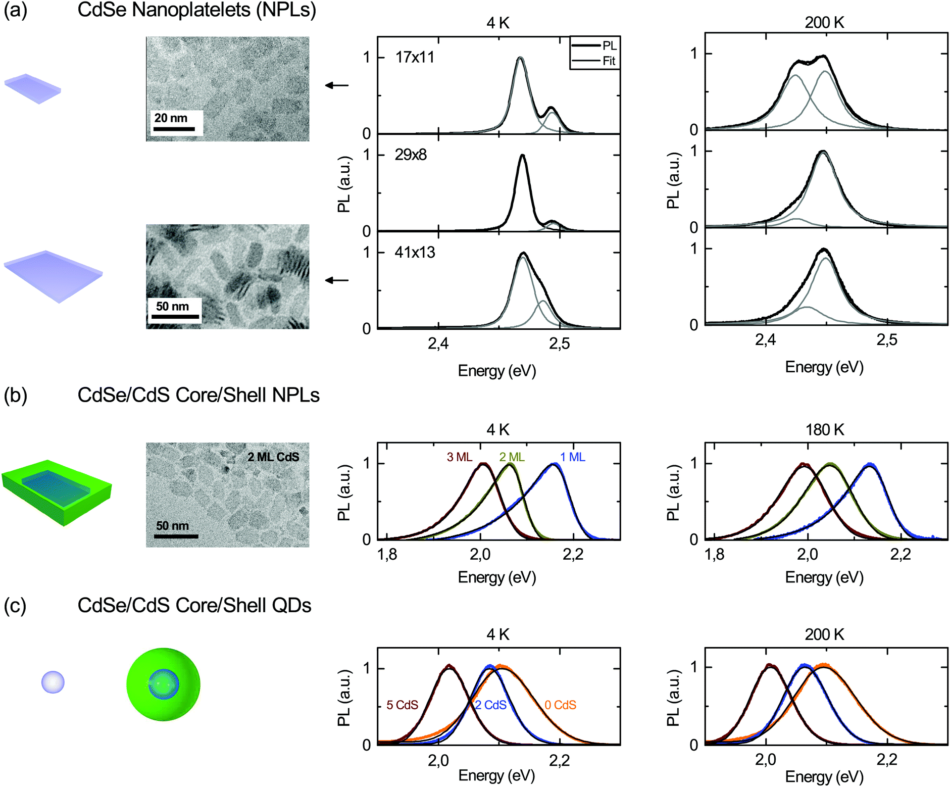 | ||
| Fig. 1 PL emission of (a) 4.5 ML core-only platelets with varying lateral sizes, (b) CdSe 1 to 3 ML (CdS) CdSe/CdS core/shell nanoplatelets, and (c) CdSe/CdS core/shell quantum dots at 4 K and 180 or 200 K as well as representative TEM images. Clearly a splitting can be observed for the core-only nanoplatelets (a) at low temperatures in line with ref. 7. PL from core-only platelets is fitted with two Voigt profiles, and core/shell particles with a modified Gaussian (black lines atop experimental curves). | ||
The increasing redshift with shell thickness (at fixed temperature) in (b) and (c) can be attributed to a lowering of the confinement related to lower conduction and valence band offsets resulting in increasing delocalization of the CdSe core exciton into the CdS shell of the heterostructures. In CdSe–CdS core–shell nanoplatelets it has been shown that still type I band alignment is maintained,12 so that our observed redshift here is not an effect of strongly different spatial electron and hole localizations, but the band alignment.
CdSe core-only nanoplatelets
We first concentrate on the CdSe core-only nanoplatelets. In line with recent results7 we observe for the core-only platelets a double emission with 20–40 meV energy spacing. Fig. 2(a) shows the temperature dependence of the centers of the double emission, obtained from Voigt fits (shown in Fig. 1) in the range of 4 to 300 K. We refer to the lower energy peak as the ground state (GS) and the higher one as the excited state (ES), without any presumptive attribution to the nature of the states. We would like to point out here that their origin – excited and ground state excitons, an exciton plus trion or an exciton plus an LO phonon replica – is still under debate.7,21,47 However, this does not affect our bandgap analysis, since both states show the same temperature dependence of the bandgap (Fig. 2a). Hence, we concentrate on the results for the energetically higher emission for the core-only sample. Furthermore, studying the emission dynamics of CdSe nanoplatelets, Biadala et al.20 recently demonstrated a dark–bright state fine structure with energy splittings of about 5 meV. Even for the presence of a higher bright and a lower dark state, Shornikova et al.34 have shown that the quasi dark exciton state does not contribute relevantly to the PL emission above 10 K resulting in no relevant impact on our measurements.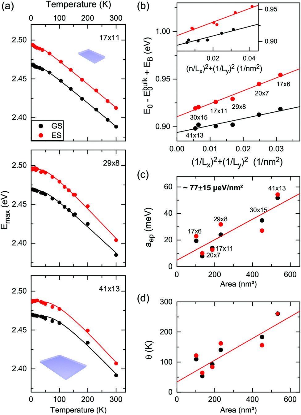 | ||
| Fig. 2 (a) Temperature dependent excitonic bandgap of 4.5 ML core-only nanoplatelets with different lateral sizes obtained from the Voigt fits in Fig. 1. Solid lines are fits according to eqn (1) in order to obtain: (b) lateral confinement part of the zero temperature excitonic bandgap versus (1/Lx)2 + (1/Ly)2 with Lx,y the lateral platelet dimensions. The inset shows the same data plotted against (n/Lx)2 + (1/Ly)2, with n = 1 for the GS and n = 2 for the ES. (c) The exciton–phonon coupling aep and (d) the average phonon temperature θ. | ||
An initial observation for the nanoplatelets (Fig. 2a) is the steeper redshift (high temperature slope) for increasing lateral platelet size (area). At first we concentrate on the lateral size dependence of the temperature-dependent bandgap shift and exciton phonon coupling. Fits to a semi-empirical model for the bandgap shift are given by48,49
 | (1) |
Using eqn (1) allows the analysis of the impact of lateral confinement on the zero temperature excitonic bandgap E0 of CdSe nanoplatelets at low temperature as shown in Fig. 2(b). Starting from the approximate expression for the confinement energy related bandgap shift ΔE of an infinitely deep semiconductor quantum box in x, y and transversal z direction the observed bandgap is
 | (2) |
A plot of dE = Eg − Eg,bulk + EBversus (1/Lx)2 + (1/Ly)2 assuming (1,1,1) for the upper and lower emission states from Fig. 1 is shown in Fig. 2. A linear dependence is fitted in this plot (R2 = 0.98). The slope π2ℏ2/2Mx,y corresponds to the quasi-particle (e.g. exciton) mass. The different slopes for the upper and lower emission indicate different masses of the emitting species, inferring different species or ground and excited states. A plot under the assumption of ground state (GS) (1,1,1) and excited state (ES) (2,1,1) excitons leads to less good correlation (R2 = 0.94) for a fit to the shifts vs. (n/Lx)2 + (1/Ly)2 and is shown in the inset of Fig. 2(b). However, a definite answer to which of the two models applies cannot be given based on the lateral confinement. As shown in the ESI,† comparing Mx,y to the literature values of the effective carrier masses in ZB CdSe for excitons, positive and negative trions and biexcitons and the ES and GS hypothesis also do not result in a final attribution. One possible scenario for the double emission discussed based on the displayed results here is an exciton and biexciton state.
Fig. 2(b) also allows us to extrapolate the energy difference of the two states for laterally infinite platelets or sheets as the difference of the intersection points of the fit curves with the ordinate. The extrapolation to laterally infinite platelets with vanishing lateral confinement results in an energy spacing of 17 meV. From the two fit curves in Fig. 2(b) the area dependent energy spacing can be given as
| ΔE[eV] = 1.600 × 10⁻² + 0.652·(1/Lx2 + 1/Ly2), | (3) |
Fig. 2(c) shows the electron–phonon coupling parameter aep obtained from the temperature-dependence of the bandgap according to eqn (1). For both, the ES and GS, aep tends to increase linearly with the platelet area -with some scattering of the data, perhaps due to not identical sample quality. A linear fit to all data (with non-zero offset) yields a slope of 77 ± 15 μeV nm−2.
A possible explanation for this linear increase is the coherent delocalization of the 2D excitons over the whole nanoplatelets. The number of unit cell dipole moments contributing to the exciton transition dipole moment increases with the platelet area via the giant oscillator strength effect (GOST).50 These elementary dipole moments coherently add up to the transition dipole moment of the exciton, which then couples to the phonon modes, leading to a linear increase of the coupling strength with the platelet area. Clear indications for this coherent delocalization over the whole nanoplatelet and the resulting increase of the transition rates in our size range of nanoplatelets have been found in ref. 8 and 10. In particular the scaling of the transition rates with the platelet area leads to a quadratic area (volume) scaling of the two photon absorption cross section with the lateral platelet size as well as a constant intrinsic absorption in the continuum. We remark that these effects of coherent delocalization are observed, as the nanoplatelets are atomically flat systems51 due to their anisotropic colloidal synthesis. In contrast epitaxial quantum wells suffer e.g. from interface roughness effects, which limit the spatial coherence of excitons more strongly.
We remark that the trend of increased exciton–phonon coupling is also observed, if aep is converted in the dimensionless Huang–Rhys parameter S, often used to quantify the strength of phonon coupling, and that the resulting values are comparable to laterally quasi infinite 2D transition dichalcogenide materials52,53 (see the ESI†).
The linear increase of aep shown in Fig. 2(c) allows for a control of electron–phonon interaction and the accompanied temperature-dependent bandgap red shift with the platelet area. Additionally, it directly implies control over dephasing in the system, as discussed later. Furthermore, this degree of freedom is practically independent of the emission energy of the system – the bandgap shifts are less than 30 meV and small compared to the ∼2.5 eV band gap that is controlled by the platelets’ thickness.
Fig. 2(d) shows the average phonon temperature θ. It corresponds to a weighted average phonon energy of acoustic and optical modes. The observed increase of θ with lateral size may be related to alterations in the average coupling to acoustic and optical phonons. It can be shown (later) that the coupling to acoustic phonons in 2D systems scales with 1/A (A being the platelet area), so that the contribution of acoustic modes is reduced with increasing platelet size. At the same time the contribution of optical modes increases. Since these exhibit energies higher than acoustic modes, the average phonon energy (temperature) increases with lateral size.
CdSe/CdS core/shell nanoplatelets and dots
In the following section we concentrate on the CdSe/CdS core/shell nanoplatelet and quantum dot samples. Fig. 3(a) and (b) compare the temperature dependent excitonic band gaps Emax deduced from fits to the PL (Fig. 1) and fitted with eqn (1). The CdSe/CdS platelet values presented here for comparison are in agreement with those recently obtained on CdSe/CdS NPLS.12Fig. 3(c) and (d) show the resulting exciton–phonon coupling aep, and (e) and (f) the average phonon temperatures θ.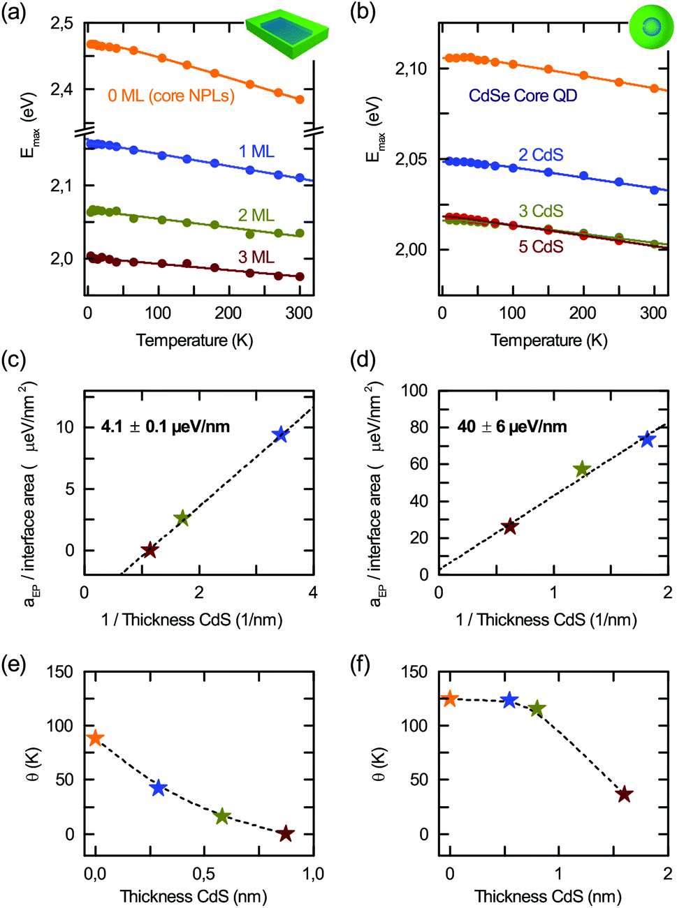 | ||
| Fig. 3 Temperature dependent excitonic bandgaps deduced from fits to PL in Fig. 1 for 4.5 ML core/shell nanoplatelets (a) and 4 nm diameter CdSe core/shell dots (b) with 0–3 ML and 0–5 ML CdS shell, respectively. Exciton–phonon coupling aep per interface area for the platelets (c) and dots (d) versus the inverse CdS thickness. For the platelets the system has two interfaces as well as their average phonon temperature θ (e) + (f) determined from fits in (a) and (b). | ||
As seen in the case of core-only platelets in Fig. 2(c), the exciton–phonon interaction aep is linear in the platelet area A. On the other hand, the density of states in a 2D system is proportional to 1/d (inverse thickness) and alters the interaction strength. For this reason, we plot in Fig. 3(c) the interaction strength per CdSe nanoplatelet area versus 1/dCdS, the CdS layer thickness. The slope is equivalent to plotting aep per surface area (2A) versus the inverse total CdS thickness of 2dCdS. For quantum dots shown in Fig. 3(d) we use the interface area given by 4π(d/2)2, with the core diameter d. We observe a linear dependence with a slope of 4.1 ± 0.1 μeV nm−1 for the core/shell platelets and 40 ± 6 μeV nm−1 for the core/shell dots.
Thus – in addition to the lateral size – a CdS shell also allows for controlling the exciton–phonon interaction in CdSe nanoplatelets and dots, in line with the first indications in ref. 12 and 42 in PL and Raman spectroscopy. Interestingly, the same concept applies to topologically similar core/shell quantum dots, which can be considered as spherical 2D CdSe/CdS interface structures, where the interaction is proportional to the interaction (interface) area. A decreasing coupling with CdS shell thickness is consistent with the results of Lin et al.,42 who observed in Raman measurements that the Huang–Rhys factor for LO-phonon coupling tended to decrease upon introduction of a shell. There, a model assuming a Fröhlich-only mechanism was not able to reproduce this trend. They offer surface charging and related S- and P-type wavefunction mixing as a possible mechanism for increasing the e–h separation and counteracting the Fröhlich coupling trend. Finally, considering the slopes in Fig. 3(c) and (d), the exciton–phonon interaction per unit area in CdSe/CdS nanoplatelets is lower than that in CdSe/CdS dots. We remark that as the platelets exhibit type I band alignment,12 there are no effects of spatially indirect exciton formation, which alters the coupling to phonons. For CdSe–CdS dots type I band alignment is also suggested,54 but is still under discussion.55
The performed renormalization by the surface area is also substantiated by the results of Takagahara et al.56 for spherical CdSe core-only quantum dots. They found a 1/r2 ∝ 1/A dependence for coupling in dots, where r is the crystallite radius. In Fig. 3(e) and (f), we further observe a reduction of the average phonon temperature with increasing CdS thickness. While the starting point for core-only samples is comparable for platelets and dots, the decrease is faster for platelets. This difference can be attributed to the different phonon densities of states for the 2D system and the spherical CdSe/CdS hetero system, so that a different scaling of the coupling to acoustic and optical modes may be the reason for these findings. As for the core-only platelets we recalculated from Fig. 3(c)–(f) the Huang–Rhys parameter S (see Fig. S1 in the ESI†) and found that S decreases with the CdS thickness in line with Fig. 3(c) and (d).
Based on an analysis of the emission line width, we will now investigate the acoustic and optical phonon coupling in more detail.
Linewidth
Fig. 4(a) shows the temperature dependent linewidth (FWHM) obtained from the log-normal function fits to the PL spectra in Fig. 1. We fit the temperature dependence with the well known expression | (4) |
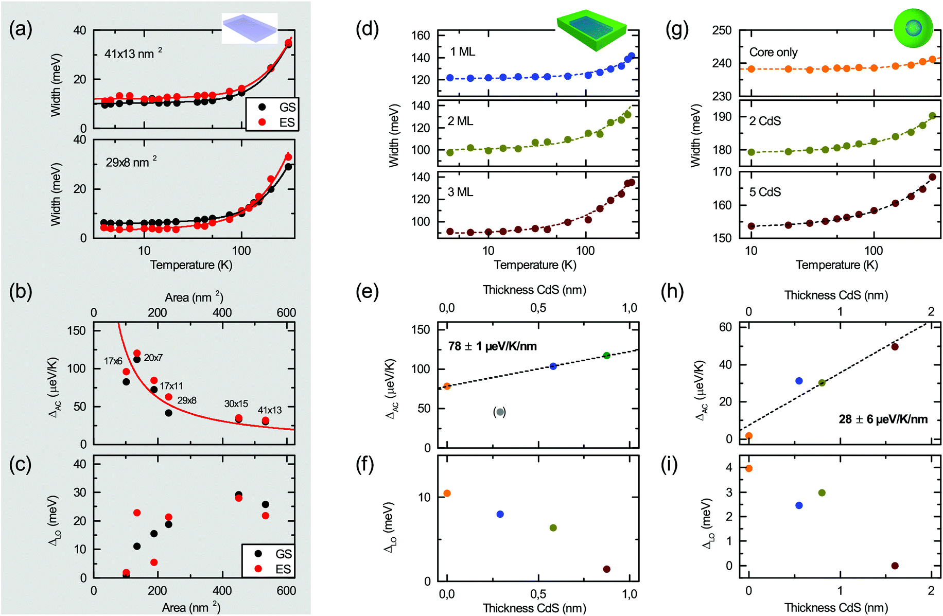 | ||
| Fig. 4 Temperature dependent line width of CdSe platelets (a), CdSe/CdS nanoplatelets (17 × 11 nm2 CdSe core) (d) and nano-dots with 4 nm core size (g), with fits to eqn (4). Resulting acoustic ΔAC (b) and LO phonon ΔLO (c) contribution to the linewidth as a function of the nanoplatelet area. (b) shows a 1/A fit according to eqn (5). (e, h) and (f, i) acoustic ΔAC and LO phonon ΔLO contribution for core/shell platelets and dots versus the CdS layer thickness. | ||
The results for core-only nanoplatelets are shown in Fig. 4(b) and (c). While there is a clear trend of a reduction of ΔAC with the platelet area, only a by trend increase is observed for ΔLO. Both trends are in line with the results in Fig. 2(d), where with increasing lateral size LO phonons provide increasingly major contribution to the average phonon temperature. θ approaches the LO phonon temperature of ∼300 K (equal to 25.4 meV) for large platelets. The demonstrated strong area scaling of the acoustic phonon interaction can be understood from the underlying theory of deformation potential interaction58,59 of acoustic phonons. According to Fermi's golden rule the transition rate Γ is proportional to the absolute value squared of transition matrix element. The effective deformation potential coupling uDP = (De − Dh)(ℏq/2Ωρνs)1/2 relates the phonon wave number q (absolute value of the wave vector), the volume Ω of the structure under consideration, the density ρ, the sound velocity vs and the deformation potential difference of De − Dh of electrons and holes. The corresponding matrix element is Mk,k′ = (De − Dh)(ℏq/2Ωρνs)1/2f(q)δk,k′+q. f(q) is the form factor that can be shown59 to be (1 + (qaB/4))−3/2 for a hydrogen (S-)like lowest envelope function and small acoustic phonon wave vectors, as estimated from ref. 7 and 60.
Due to Fermi's golden rule the transition rate Γ scales with the square of uDP. In our platelets with dimensions Lx,y,z and volume Ω = LxLyLz, the quantized phonon wave vector is q = π(1/Lx2 + 1/Ly2 + 1/Lz2)1/2. Following ref. 61 and 59, and assuming small acoustic phonon wave vectors (as e.g. also shown in ref. 62), the third contribution is the dominant one and is given by the z-breathing mode frequency (taken from ref. 60) since Lx,Ly ≫ Lz. The contribution of acoustic phonon scattering to the homogeneous line width is Δacoust = 2ℏΓ.10 Since according to eqn (4)Δacoust(T) = ΔACT, this leads, apart from a scaling factor CDP, to the following dependency
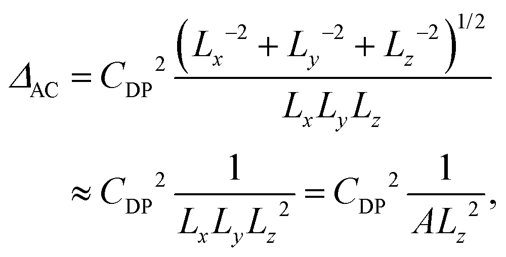 | (5) |
Slight deviations of the actual platelets from the fit curve in Fig. 4(b) may be related to slight variation of sample quality or size determination by TEM.
We remark that the observed trend of a decrease of acoustic phonon coupling with nanostructure size is in-line with calculations by Kelley66 and Takagahara et al.56 for spherical CdSe quantum dots. With increasing size the exciton coupling to acoustic phonons was observed to decrease due to decreasing deformation potential coupling. Our results for large platelets are comparable to large dots, for which Takagahara et al. found the coupling to be about 7 μeV K−1. For small quantum dots, of diameter comparable to the thickness of our 4.5 ML platelets (1.4 nm), they obtained ∼100 μeV K−1 – in good agreement with the values of smaller platelets as shown in Fig. 4(b). We also note that they found a 1/r2 dependence for dots, where r is the crystallite radius. This corresponds to an inverse surface area dependence of the nanocrystal analogous to our findings for the nanoplatelets (∝1/A).
This inverse relationship between coupling to low energy acoustic modes and platelet area A further substantiates our interpretation of the increase of the average phonon temperature θ as shown in Fig. 2(d) with A. For larger lateral sizes the contribution of low energy acoustic modes decreases due to the reduced coupling while optical modes with higher phonon energies increasingly contribute to the average phonon temperature.
In Fig. 4(c) we further observe a by trend increase of the coupling to LO-phonons with increasing nanoplatelet area. The coupling to optical modes tends to increase with A and then saturate for large platelet areas towards values reported by Chia et al. for laterally infinite MBE grown CdSe epilayers (≈20 meV).67 As the Fröhlich interaction is considered the dominating mechanism42 for the LO phonon coupling in polar semiconductor nano-structures we briefly investigate whether this can explain the observed complicated behavior directly. The corresponding interaction potential59 results in a predicted scaling ΔLO ∝ (1/Lx2 + 1/Ly2 + 1/Lz2)−1LxLyLz ∝ A/2Lz[(Lx − Ly)2 + A], where the first proportionality is an approximation due to Lx,Ly ≫ Lz and the last proportionality due to Lx ∼ Ly for fixed well width Lz. A nonlinear increase for larger platelet areas is expected for more quadratic nanoplatelets. The observed scatter of data points may be related to the lateral aspect ratio sensitivity (via the (Lx − Ly)2 dependence), as the used platelets have varying aspect ratios. However, the actual trend in Fig. 4(c) cannot be fully explained by this simple theory. Another explanation for deviations from the simple scaling theory presented could be a varying defect density which alters the LO phonon coupling, as e.g. the number of defect sites scales with the platelet area. A detailed analysis, however, is beyond the scope of this article.
In the following we analyze the cases of CdSe/CdS platelets and dots for varying CdS layer thicknesses. Fig. 4(e) and (f) show the coupling to acoustic and optical modes. ΔAC can be (roughly) approximated with a linear increase with the CdS layer thickness. The 1 ML CdS sample is excluded from the linear fit shown in Fig. 3(e). The trend – which is in line with the reduction of the average phonon temperature in Fig. 3(c + d)via increasing coupling to low energy acoustic phonons – may be interpreted in terms of an increase of the interaction volume with increasing shell thickness. In bulk the acoustic branches of the phonon dispersion in CdSe and CdS are quite similar and have a continuous spectrum. Here we have quantized acoustic modes, but the energy spectrum is still quite similar in both materials, which can be seen from the fact that the acoustic sound velocities 2.3 km s−1 and 2.6 km s−1 for CdSe and CdS (calculated based on ref. 60) are quite similar. Hence there is no strong mode confinement due to the CdSe–CdS interface and to a first approximation the acoustic modes can be considered as to extend over the whole particle, including the CdS shell. In contrast these arguments do not apply to the optical modes, as the energies of LO phonons in CdSe (∼210 cm−1) and CdS (∼302 cm−1) are well distinct. Hence, an increased shell thickness and wavefunction delocalization may tend to decrease the LO coupling as the core (LO) phonon modes cannot couple to the shell modes and the wavefunction overlap of the exciton with the core mode decreases relatively for stronger delocalization into thicker CdS shells.
A reduction of the coupling to LO phonons is further observed in (f). Lin et al.42 measured a non Fröhlich-like reduction of the coupling (Huang–Rhys factor S) with increasing shell thickness in CdSe/CdS quantum dots – in-line with our result. This seems to be a universal trend in hetero-nanoplatelets and quantum dots. Furthermore, the decreasing coupling to high energy LO-phonons with increasing layer thickness is also reflected in the reduction of the average phonon temperature θ as seen in Fig. 3(e) and (f). This also confirms the consistency of our whole analysis via the independent experimental quantities, bandgap and line width.
The same trends of acoustic and optical phonon coupling with CdS shell thickness discussed now for platelets (Fig. 4(e + f)) are also observed for the topologically similar CdSe/CdS dots. On an absolute scale, they show smaller coupling than nanoplatelets. This may stem from smaller transition dipole moments in dots as compared to platelets coupling to phonons, or a not perfect spherical shape of the nanoparticles. The dots are smaller than the nanoplatelets. This may result in a smaller number of acoustic or LO-phonon modes in the system to which the exciton can couple, leading to an overall reduction in CdSe/CdS dots compared to platelets. Furthermore, due to different crystallographic orientations on the dot surface, CdS monolayers are not as ideally smooth as on the platelets, which may result e.g. in the larger data point scatter.
The demonstration of the tuneability of exciton–phonon interaction in colloidal quantum-wells by lateral size and shell growth has strong application potential, for example, for tuning carrier cooling, which is relevant e.g. in solar energy harvesting applications. Furthermore, carrier multiplication is a very active field, where carrier cooling and carrier multiplication are competing processes. The former tunes the multi-carrier pair generation efficiencies and poses a promising way to boost solar cell efficiencies. Hence 2D materials of finite lateral size, like the nanoplatelets in this manuscript, with a control of the carrier cooling rates are desirable model systems, for both basic understanding of the involved processes as well as optimization of the performance of solar energy converters. Also for transport in nanosystems our results show the feasibility of tuning exciton–phonon interaction, for example in field-effect transistors, varying the lateral size of the structure and e.g. tuning from ballistic to diffusive transport. A further interesting implication of our results is that the quantum yield of nanoplatelets with or without a shell, which has been found to be considerably different,12 will depend on the phonon interaction, which governs exciton cooling and relaxation in non-radiative channels. For large platelets or core/shell platelets with thin shells the average phonon coupling is the highest, so that e.g. phonon assisted nonradiative recombination is stronger. These findings can be used for emitters of optimized photoluminescence efficiency. Our results open up a new toolbox for the design of photonic materials.
Conclusion
In summary we have shown that CdSe nanoplatelets possess a lateral confinement of ∼30 meV, which can be adjusted via the lateral size of the nanoplatelets. We demonstrated that exciton–phonon coupling in CdSe nanoplatelets can be varied strongly via the lateral size or the thickness of a CdS shell. The coupling to acoustic phonons decreases with the platelet area by a factor of ∼4, in line with deformation potential theory. The resulting −3.03 eV exciton–acoustic phonon deformation potential is in line with theory predictions. The coupling to LO-phonons is observed to decrease with decreasing platelet area. We further demonstrated that a CdS shell results in an increased coupling to acoustic modes and reduced coupling to optical modes for both CdSe–CdS core–shell platelets and quantum dots. The absolute coupling strengths are lower for quantum dots than for nanoplatelets, which may be attributed to the higher transition dipole moments to which the phonon modes couple in nanoplatelets and more phonon modes to couple to in the larger nanoplatelets. We further demonstrated that the average exciton–phonon coupling strength increases linearly with the platelet area for core-only platelets, while it is linear in the interface area versus the inverse CdS layer thickness in core/shell platelets as well as in nanodots. As the trends for both core/shell structures are similar, there is a universal mechanism for 2D platelets and similar core–shell dots also exhibiting a 2D interface. Our results regarding the tunability of phonon interaction are of immediate interest for carrier cooling and multiexciton generation, relevant for solar light conversion, for transport and high quantum yield emitters and open up a new toolbox for the design of photonic materials. We remark that further in-depth studies beyond the scope of this article are necessary to give a definite answer to the nature of the two emissive states in CdSe nanoplatelets, however our experimental results presented in this paper are not influenced by this.Methods
Synthesis and characterization
TEM analysis of all samples was performed through different instruments (Jeol ARM200F operated at 200 kV and Zeiss Leo 906E at 120 kV). At least 50 platelets per sample were used for size determination.
Conflicts of interest
There are no conflicts to declare.Acknowledgements
R. S., U. W. and A. W. A acknowledge the DFG grants WO477-1/32 and AC290-2/1., M. A. the CHEMREAGENTS program, and A. A. the BRFFI grant no. X17KIG-004.References
- F. Gerdes, C. Navío, B. H. Juárez and C. Klinke, Nano Lett., 2017, 17, 4165–4171 CrossRef CAS PubMed.
- J. Joo, J. S. Son, S. G. Kwon, J. H. Yu and T. Hyeon, J. Am. Chem. Soc., 2006, 128, 5632–5633 CrossRef CAS.
- S. Ithurria and B. Dubertret, J. Am. Chem. Soc., 2008, 130, 16504–16505 CrossRef CAS PubMed.
- A. W. Achtstein, A. Schliwa, A. Prudnikau, M. Hardzei, M. V. Artemyev, C. Thomsen and U. Woggon, Nano Lett., 2012, 12, 3151–3157 CrossRef CAS.
- Q. Wang, K. Kalantar-Zadeh, A. Kis, J. Coleman and M. Strano, Nat. Mater., 2012, 699–712 CAS.
- A. Steinhoff, M. Florian, A. Singh, K. Tran, M. Kolarczik, S. Helmrich, A. W. Achtstein, U. Woggon, N. Owschimikow, F. Jahnke and X. Li, Nat. Phys., 2018, 14, 1199 Search PubMed.
- A. W. Achtstein, R. Scott, S. Kickhöfel, S. T. Jagsch, S. Christodoulou, G. H. Bertrand, A. V. Prudnikau, A. Antanovich, M. Artemyev, I. Moreels, A. Schliwa and U. Woggon, Phys. Rev. Lett., 2016, 116, 116802 CrossRef PubMed.
- J. Planelles, A. W. Achtstein, R. Scott, N. Owschimikow, U. Woggon and J. I. Climente, ACS Photonics, 2018, 5, 3680–3688 CrossRef CAS.
- S. Ithurria, M. D. Tessier, B. Mahler, R. P. S. M. Lobo, B. Dubertret and A. L. Efros, Nat. Mater., 2011, 10, 936–941 CrossRef CAS PubMed.
- A. Naeem, F. Masia, S. Christodoulou, I. Moreels, P. Borri and W. Langbein, Phys. Rev. B: Condens. Matter Mater. Phys., 2015, 91, 121302 CrossRef.
- A. Polovitsyn, Z. Dang, J. L. Movilla, B. Martín-García, A. H. Khan, G. H. V. Bertrand, R. Brescia and I. Moreels, Chem. Mater., 2017, 29, 5671–5680 CrossRef CAS.
- A. W. Achtstein, O. Marquardt, R. Scott, M. Ibrahim, T. Riedl, A. V. Prudnikau, A. Antanovich, N. Owschimikow, J. K. N. Lindner, M. Artemyev and U. Woggon, ACS Nano, 2018, 12, 9476–9483 CrossRef CAS.
- C. She, I. Fedin, D. S. Dolzhnikov, A. Demortière, R. D. Schaller, M. Pelton and D. V. Talapin, Nano Lett., 2014, 14, 2772–2777 CrossRef CAS.
- J. Q. Grim, S. Christodoulou, F. Di Stasio, R. Krahne, R. Cingolani, L. Manna and I. Moreels, Nat. Nanotechnol., 2014, 9, 891–895 CrossRef CAS.
- M. Li, M. Zhi, H. Zhu, W.-Y. Wu, Q.-H. Xu, M. Hyphong Jhon and Y. Chan, Nat. Commun., 2015, 6, 8513 CrossRef CAS PubMed.
- R. Scott, A. W. Achtstein, A. Prudnikau, A. Antanovich, S. Christodoulou, I. Moreels, M. Artemyev and U. Woggon, Nano Lett., 2015, 15, 4985–4992 CrossRef CAS PubMed.
- J. Heckmann, R. Scott, A. V. Prudnikau, A. Antanovich, N. Owschimikow, M. Artemyev, J. I. Climente, U. Woggon, N. B. Grosse and A. W. Achtstein, Nano Lett., 2017, 17, 6321–6329 CrossRef CAS PubMed.
- R. Scott, J. Heckmann, A. V. Prudnikau, A. Antanovich, A. Mikhailov, N. Owschimikow, M. Artemyev, J. I. Climente, U. Woggon, N. B. Grosse and A. W. Achtstein, Nat. Nanotechnol., 2017, 1155–1160 CrossRef CAS.
- D.-E. Yoon, W. D. Kim, D. Kim, D. Lee, S. Koh, W. K. Bae and D. C. Lee, J. Phys. Chem. C, 2017, 121, 24837–24844 CrossRef CAS.
- L. Biadala, F. Liu, M. D. Tessier, D. R. Yakovlev, B. Dubertret and M. Bayer, Nano Lett., 2014, 14, 1134–1139 CrossRef CAS PubMed.
- E. V. Shornikova, L. Biadala, D. R. Yakovlev, V. F. Sapega, Y. G. Kusrayev, A. A. Mitioglu, M. V. Ballottin, P. C. M. Christianen, V. V. Belykh, M. V. Kochiev, N. N. Sibeldin, A. A. Golovatenko, A. V. Rodina, N. A. Gippius, A. Kuntzmann, Y. Jiang, M. Nasilowski, B. Dubertret and M. Bayer, Nanoscale, 2018, 10, 646–656 RSC.
- R. Scott, A. W. Achtstein, A. V. Prudnikau, A. Antanovich, L. D. A. Siebbeles, M. Artemyev and U. Woggon, Nano Lett., 2016, 16, 6576–6583 CrossRef CAS PubMed.
- R. Benchamekh, N. A. Gippius, J. Even, M. O. Nestoklon, J.-M. Jancu, S. Ithurria, B. Dubertret, A. L. Efros and P. Voisin, Phys. Rev. B: Condens. Matter Mater. Phys., 2014, 89, 035307 CrossRef.
- M. Richter, Phys. Rev. Mater., 2017, 1, 016001 CrossRef.
- F. Rajadell, J. I. Climente and J. Planelles, Phys. Rev. B, 2017, 96, 035307 CrossRef.
- S. Christodoulou, J. I. Climente, J. Planelles, R. Brescia, M. Prato, B. Martin-Garcia, A. H. Khan and I. Moreels, Nano Lett., 2018, 18, 6248–6254 CrossRef CAS PubMed.
- R. Scott, S. Kickhofel, O. Schoeps, A. Antanovich, A. Prudnikau, A. Chuvilin, U. Woggon, M. Artemyev and A. W. Achtstein, Phys. Chem. Chem. Phys., 2016, 18, 3197–3203 RSC.
- A. G. Kelly, T. Hallam, C. Backes, A. Harvey, A. S. Esmaeily, I. Godwin, J. Coelho, V. Nicolosi, J. Lauth, A. Kulkarni, S. Kinge, L. D. A. Siebbeles, G. S. Duesberg and J. N. Coleman, Science, 2017, 356, 69–73 CrossRef CAS PubMed.
- A. W. Achtstein, A. V. Prudnikau, M. V. Ermolenko, L. I. Gurinovich, S. V. Gaponenko, U. Woggon, A. V. Baranov, M. Y. Leonov, I. D. Rukhlenko, A. V. Fedorov and M. V. Artemyev, ACS Nano, 2014, 8, 7678–7686 CrossRef CAS PubMed.
- A. Chu, C. Livache, S. Ithurria and E. Lhuillier, J. Appl. Phys., 2018, 123, 035701 CrossRef.
- A. Prudnikau, A. Chuvilin and M. Artemyev, J. Am. Chem. Soc., 2013, 135, 14476–14479 CrossRef CAS PubMed.
- A. V. Antanovich, A. V. Prudnikau, D. Melnikau, Y. P. Rakovich, A. Chuvilin, U. Woggon, A. W. Achtstein and M. V. Artemyev, Nanoscale, 2015, 7, 8084–8092 RSC.
- Y. Kelestemur, B. Guzelturk, O. Erdem, M. Olutas, K. Gungor and H. V. Demir, Adv. Funct. Mater., 2016, 26, 3570–3579 CrossRef CAS.
- E. V. Shornikova, L. Biadala, D. R. Yakovlev, D. Feng, V. F. Sapega, N. Flipo, A. A. Golovatenko, M. A. Semina, A. V. Rodina, A. A. Mitioglu, M. V. Ballottin, P. C. M. Christianen, Y. G. Kusrayev, M. Nasilowski, B. Dubertret and M. Bayer, Nano Lett., 2018, 18, 373–380 CrossRef CAS PubMed.
- R. Pandya, R. Y. S. Chen, A. Cheminal, M. Dufour, J. M. Richter, T. H. Thomas, S. Ahmed, A. Sadhanala, E. P. Booker, G. Divitini, F. Deschler, N. C. Greenham, S. Ithurria and A. Rao, J. Am. Chem. Soc., 2018, 140, 14097–14111 CrossRef CAS PubMed.
- J. Zhao, J. A. Bardecker, A. M. Munro, M. S. Liu, Y. Niu, I.-K. Ding, J. Luo, B. Chen, A. K.-Y. Jen and D. S. Ginger, Nano Lett., 2006, 6, 463–467 CrossRef CAS PubMed.
- Y. Zeng and D. F. Kelley, J. Phys. Chem. C, 2016, 120, 17853–17862 CrossRef CAS.
- M. Nasilowski, P. Spinicelli, G. Patriarche and B. Dubertret, Nano Lett., 2015, 15, 3953–3958 CrossRef CAS PubMed.
- K. Gong, J. E. Martin, L. E. Shea-Rohwer, P. Lu and D. F. Kelley, J. Phys. Chem. C, 2015, 119, 2231–2238 CrossRef CAS.
- M. Cirillo, T. Aubert, R. Gomes, R. Van Deun, P. Emplit, A. Biermann, H. Lange, C. Thomsen, E. Brainis and Z. Hens, Chem. Mater., 2014, 26, 1154–1160 CrossRef CAS.
- C. Gollner, J. Ziegler, L. Protesescu, D. N. Dirin, R. T. Lechner, G. Fritz-Popovski, M. Sytnyk, S. Yakunin, S. Rotter, A. A. Yousefi Amin, C. Vidal, C. Hrelescu, T. A. Klar, M. V. Kovalenko and W. Heiss, ACS Nano, 2015, 9, 9792–9801 CrossRef CAS PubMed.
- C. Lin, K. Gong, D. F. Kelley and A. M. Kelley, ACS Nano, 2015, 9, 8131–8141 CrossRef CAS PubMed.
- J. Cui, A. P. Beyler, I. Coropceanu, L. Cleary, T. R. Avila, Y. Chen, J. M. Cordero, S. L. Heathcote, D. K. Harris, O. Chen, J. Cao and M. G. Bawendi, Nano Lett., 2016, 16, 289–296 CrossRef CAS PubMed.
- G. H. V. Bertrand, A. Polovitsyn, S. Christodoulou, A. H. Khan and I. Moreels, Chem. Commun., 2016, 52, 11975–11978 RSC.
- S. Ithurria and D. V. Talapin, J. Am. Chem. Soc., 2012, 134, 18585–18590 CrossRef CAS PubMed.
- N. Tschirner, H. Lange, A. Schliwa, A. Biermann, C. Thomsen, K. Lambert, R. Gomes and Z. Hens, Chem. Mater., 2012, 24, 311–318 CrossRef CAS.
- M. D. Tessier, L. Biadala, C. Bouet, S. Ithurria, B. Abecassis and B. Dubertret, ACS Nano, 2013, 7, 3332–3340 CrossRef CAS PubMed.
- L. Vina, S. Logothetidis and M. Cardona, Phys. Rev. B: Condens. Matter Mater. Phys., 1984, 30, 1979–1991 CrossRef CAS.
- K. P. O'Donnell and X. Chen, Appl. Phys. Lett., 1991, 58, 2924–2926 CrossRef.
- J. Feldmann, G. Peter, E. O. Göbel, P. Dawson, K. Moore, C. Foxon and R. J. Elliott, Phys. Rev. Lett., 1987, 59, 2337–2340 CrossRef CAS PubMed.
- A. Riedinger, F. D. Ott, A. Mule, S. Mazzotti, P. N. Knusel, S. J. P. Kress, F. Prins, S. C. Erwin and D. J. Norris, Nat. Mater., 2017, 16, 743–748 CAS.
- S. Helmrich, R. Schneider, A. W. Achtstein, A. Arora, B. Herzog, S. M. de Vasconcellos, M. Kolarczik, O. Schöps, R. Bratschitsch, U. Woggon and N. Owschimikow, 2D Mater., 2018, 5, 045007 CrossRef.
- F. Cadiz, E. Courtade, C. Robert, G. Wang, Y. Shen, H. Cai, T. Taniguchi, K. Watanabe, H. Carrere, D. Lagarde, M. Manca, T. Amand, P. Renucci, S. Tongay, X. Marie and B. Urbaszek, Phys. Rev. X, 2017, 7, 021026 Search PubMed.
- Z. Ning, H. Tian, H. Qin, Q. Zhang, H. Ågren, L. Sun and Y. Fu, J. Phys. Chem. C, 2010, 114, 15184–15189 CrossRef CAS.
- L. Wang, K. Nonaka, T. Okuhata, T. Katayama and N. Tamai, J. Phys. Chem. C, 2018, 122, 12038–12046 CrossRef CAS.
- T. Takagahara, Phys. Rev. Lett., 1993, 71, 3577–3580 CrossRef CAS PubMed.
- S. A. Cherevkov, A. V. Fedorov, M. V. Artemyev, A. V. Prudnikau and A. V. Baranov, Phys. Rev. B: Condens. Matter Mater. Phys., 2013, 88, 041303 CrossRef.
- B. K. Basu, Theory of Optical Processes in Semiconductors, Oxford Univ. Press, Oxford, 1997 Search PubMed.
- C. Ndebeka-Bandou, F. Carosella and G. Bastard, Quantum States and Scattering in Semiconductor Nanostructures, World Scientiffic, 2016 Search PubMed.
- A. Girard, L. Saviot, S. Pedetti, M. D. Tessier, J. Margueritat, H. Gehan, B. Mahler, B. Dubertret and A. Mermet, Nanoscale, 2016, 8, 13251–13256 RSC.
- W. Shen and S. Shen, Infrared Phys. Technol., 1996, 37, 655–657 CrossRef CAS.
- S. Shree, M. Semina, C. Robert, B. Han, T. Amand, A. Balocchi, M. Manca, E. Courtade, X. Marie, T. Taniguchi, K. Watanabe, M. M. Glazov and B. Urbaszek, Phys. Rev. B, 2018, 98, 035302 CrossRef.
- D. O. Sigle, J. T. Hugall, S. Ithurria, B. Dubertret and J. J. Baumberg, Phys. Rev. Lett., 2014, 113, 087402 CrossRef PubMed.
- A. Antanovich, A. W. Achtstein, A. Matsukovich, A. Prudnikau, P. Bhaskar, V. Gurin, M. Molinari and M. Artemyev, Nanoscale, 2017, 9, 18042–18053 RSC.
- R. Bhargava, Properties of Wide Bandgap II-VI Semiconductors, INSPEC, Institute of Electrical Engineers, 1997 Search PubMed.
- A. M. Kelley, ACS Nano, 2011, 5, 5254–5262 CrossRef CAS PubMed.
- C. Chia, C. Yuan, J. Ku, S. Yang, W. Chou, J. Juang, S. Hsieh, K. Chiu, J. Hsu and S. Jeng, J. Lumin., 2008, 128, 123–128 CrossRef CAS.
Footnotes |
| † Electronic supplementary information (ESI) available. See DOI: 10.1039/C8NR09458F |
| ‡ These authors contributed equally to this work. |
| § Current address: Physical Chemistry, TU Dresden, Bergstraße 66b, 01062 Dresden, Germany. |
| This journal is © The Royal Society of Chemistry 2019 |