
 Open Access Article
 This Open Access Article is licensed under a Creative Commons Attribution-Non Commercial 3.0 Unported Licence
Silicon substrate effects on ionic current blockade in solid-state nanopores†
Makusu
Tsutsui
 *a,
Kazumichi
Yokota
ab,
Tomoko
Nakada
a,
Akihide
Arima
a,
Wataru
Tonomura
a,
Masateru
Taniguchi
a,
Takashi
Washio
*a and
Tomoji
Kawai
*a
*a,
Kazumichi
Yokota
ab,
Tomoko
Nakada
a,
Akihide
Arima
a,
Wataru
Tonomura
a,
Masateru
Taniguchi
a,
Takashi
Washio
*a and
Tomoji
Kawai
*a
aThe Institute of Scientific and Industrial Research, Osaka University, Japan. E-mail: tsutsui@sanken.osaka-u.ac.jp; washio@ar.sanken.osaka-u.ac.jp; kawai@sanken.osaka-u.ac.jp
bNational Institute of Advanced Industrial Science and Technology, Japan
First published on 22nd February 2019
Abstract
We investigated the roles of silicon substrate material compositions in ionic current blockade in solid-state nanopores. When detecting single nanoparticles using an ionic current in a Si3N4 nanopore supported on a doped silicon wafer, resistive pulses were found to be blunted significantly via signal retardation due to predominant contributions of large capacitance at the ultrathin membrane. Unexpectedly, in contrast, changing the substrate material to non-doped silicon led to the sharpening of the spike-like signal feature, suggesting a better temporal resolution of the cross-channel ionic current measurements by virtue of the thick intrinsic semiconductor layer that served to diminish the net chip capacitance. The present results suggest the importance of the choice of Si compositions regarding the capacitance effects to attain better spatiotemporal resolution in solid-state nanopore sensors.
Introduction
Solid-state nanopores have been widely used as a useful sensor platform for analyzing single particles and single molecules in liquid.1–5 The detection principle involves measurements of an ionic current through a nanoscale hole sculpted in a thin dielectric membrane supported usually on a Si wafer.6 This simple mechanism allows one to detect an object passing through the conduit as it excludes ions there, thereby causing a pulse-like decrease in the current. The thus recorded resistive pulse contains valuable information concerning multiple physical parameters of single particles, including volume,7,8 shape,9,10 mass,11 surface charges,12 and even surface proteins.13Similar to any sensor devices, a signal-to-noise ratio is a crucial issue in nanopore sensing. Usually, this has been dealt with by designing the channel size closer to the analytes of concern so as to produce more pronounced ionic current spikes by letting a larger amount of in-pore ion blockage upon translocation relative to the channel volume.7 Surface coating has also proven to be promising for suppressing the noise stemming from electrochemical reactions at water–dielectric interfaces14 as well as for coupling of amplifier voltage noise to device capacitance.15–18 In addition to these strategies, the choice of substrate materials has been found to be a more basic yet effective way for improving the sensitivity of single-particle detectors.19,20 For instance, compared to widely employed Si, low-k materials such as glass and polymers were demonstrated to offer a lower noise platform.19 However, non-Si substrates are not compatible in general with semiconductor technologies due to the rough surface that necessitates special skills to form membranes and pores.19 In contrast, we herein show that intrinsic Si can still be useful as a nanopore substrate regarding the spatiotemporal resolution of the ionic current-based single-particle analyses.
Results and discussion
Ionic current in a nanopore on doped Si
While the good insulating property of intrinsic Si posed a difficulty for exploiting electron-beam lithography to delineate nanopores, we developed a process to finely define a nanoscale channel by inserting a conductive thin film on a resist layer. By this process, we fabricated a pore of diameter dpore in a 50 nm thick Si3N4 membrane suspended on doped (1–20 Ω cm) or non-doped (>1000 Ω cm) Si substrates and used it for the resistive pulse analyses of carboxylated polystyrene nanoparticles of diameter dPS in an electrolyte solution.The cross-membrane ionic current Iionversus time (t) curves in 1× PBS with a nanopore of dpore = 300 nm supported on a doped Si substrate (Fig. 1, see also Fig. S1†) showed an open pore current of 61 nA. This ionic conductance is in quantitative accordance withthe analytical expression21,22 of the ionic resistance Rpore inside the channel, Rpore = ρ(4tpore/πdpore2 + 1/dpore) = 1.6 MΩ with the solution resistivity ρ = 0.4 Ω m for 1× PBS and the pore depth tpore = 50 nm predicting Iion = 62 nA at 0.1 V. On the other hand, resistive pulses were observed when admitting the buffer containing carboxylated polystyrene beads of dPS = 200 nm, which are indicative of the electrophoretic translocation of the negatively charged polymeric nanoparticles through the channel (Fig. 2a).6 A close view of an Iion signal revealed a rather smooth change in the current reflecting the dynamic motions of the polymer sphere in the expansive sensing zone extending by more than 500 nm from the channel due to the ultra-low thickness-to-diameter aspect ratio motif of the Si3N4 nanopore used (Fig. 2b and c).23
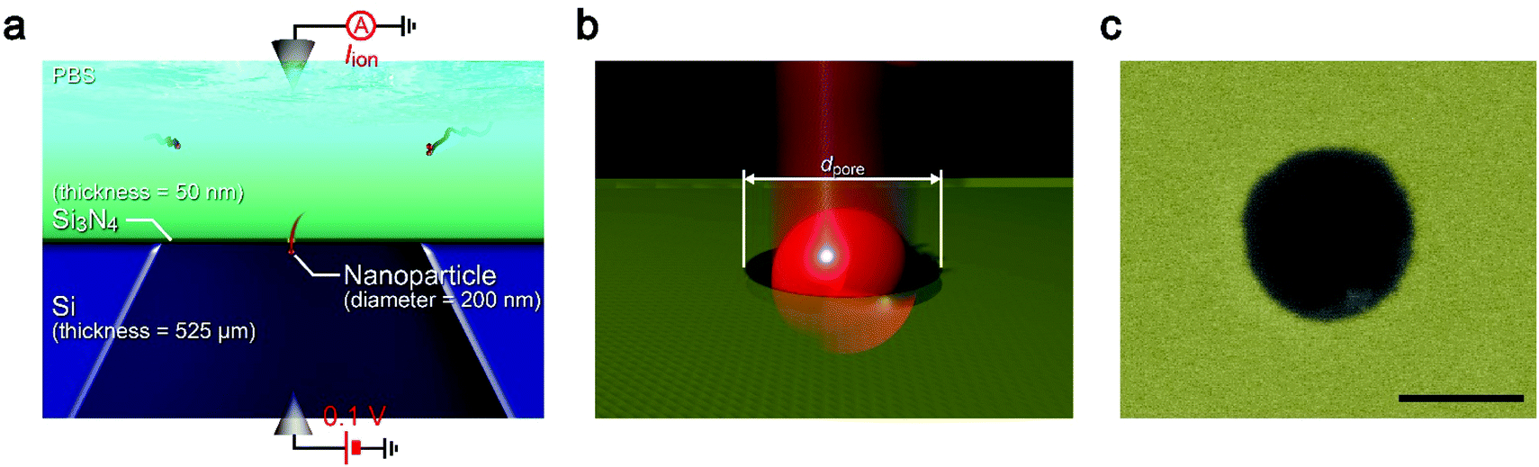 | ||
| Fig. 1 Solid-state nanopore structure. (a and b) Schematic models depicting single-nanoparticle detection in an electrolyte solution using a solid-state nanopore supported on a Si substrate. Two Ag/AgCl electrodes were utilized to apply a dc voltage of 0.1 V to a pore of diameter dpore (b) in a thin membrane and measure the ionic current Iion flowing through therein. (c) False-colored scanning electron micrograph of a nanopore of dpore = 300 nm sculpted in a 50 nm thick Si3N4 membrane. Scale bar denotes 200 nm. | ||
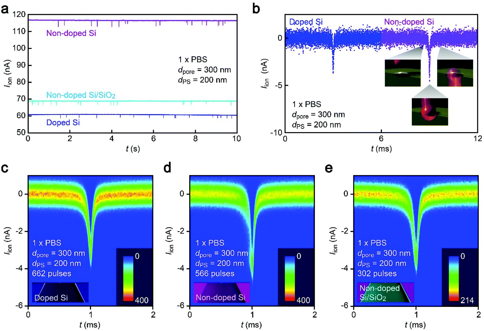 | ||
| Fig. 2 Single-nanoparticle detection using a nanopore on a Si support of various compositions. (a) Temporal change in the ionic current (Iion) through a 300 nm sized nanopore supported on a substrate made up of doped Si (blue), non-doped Si (purple), or SiO2-coated non-doped Si (sky blue) in a dispersion solution of 200 nm sized carboxylated polystyrene nanoparticles in 1× PBS. Pulse-like signals indicate the electrophoretic translocation of the nanoparticles through the nanopore. (b) Magnified views of resistive pulses. The open pore current is offset to zero. Color coding is the same as that in (a). (c–e) Two-dimensional histograms showing a number of resistive pulses obtained with a 300 nm sized nanopore supported on a substrate of doped Si (c), non-doped Si (d), and SiO2-coated non-doped Si (e). | ||
Anomalous cross-pore ionic current characteristics on non-doped Si
Unexpectedly, Iion traces of a nanopore on non-doped Si were found to be quite different. First of all, although the experimental conditions including ion concentrations and pore geometries were all set to be the same, the open pore current was higher by a factor of 2 than that in doped Si (Fig. 2a). Moreover, the ionic spike signals were also found to be slightly larger (Fig. 2b–d). This sort of difference cannot be simply ascribed to a variation in the pore diameter as larger pores should yield smaller resistive pulses in the low-thickness-to-diameter aspect ratio pore structure,23 which is opposite to the case in Fig. 2b. In fact, the pore diameter was confirmed to differ by less than 10% under a scanning electron microscope (Fig. S1†). To shed light on this intriguing material dependence of the cross-membrane ionic current, we coated a SiO2 layer of 50 nm thickness on the non-doped Si by chemical vapor deposition. Surprisingly, it caused only a marginal change in the resistive pulse waveforms from those found in the non-doped Si chips (Fig. 2e), whereas the open pore current became lower to a level comparable to that in the nanopore on doped Si (Fig. 2a; see also Fig. S2†). Similar effects have been observed by Lee and co-workers,13 wherein they attributed them to the suppression of electrochemical reactions at the Si surface. However, whether the results in Fig. 2 can also be explained by the surface effect needs further verification.Leakage current via unintentionally formed pinholes
We thus explored the physical origin of the peculiar open pore conductance (Fig. 3) by measuring the Iionversus bias voltage Vb characteristics. We investigated the salt concentration (cion) dependence of the open pore ionic conductance Gopen. By diluting 10× PBS with ultrapure water (Merck Millipore), we prepared an electrolyte solution consisting mostly of Na+ and Cl− ions with a vast range of cion from 1.4 M down to 1.4 × 10⁻⁶ M (Fig. 3a and b). The results for 1.2 μm sized Si3N4 pores showed a linear decrease in Gpore with decreasing salt concentration at cion > 10−3 M irrespective of the substrate materials manifesting the drift current characteristic of Iion derived from the electric field-driven ion transport through the conduits (Fig. 3c).24 In contrast, Gpore tended to level off at a certain level when further lowering cion. This electrolyte-independent ionic current can be attributed to predominant contributions of counterions at the pore wall surface.25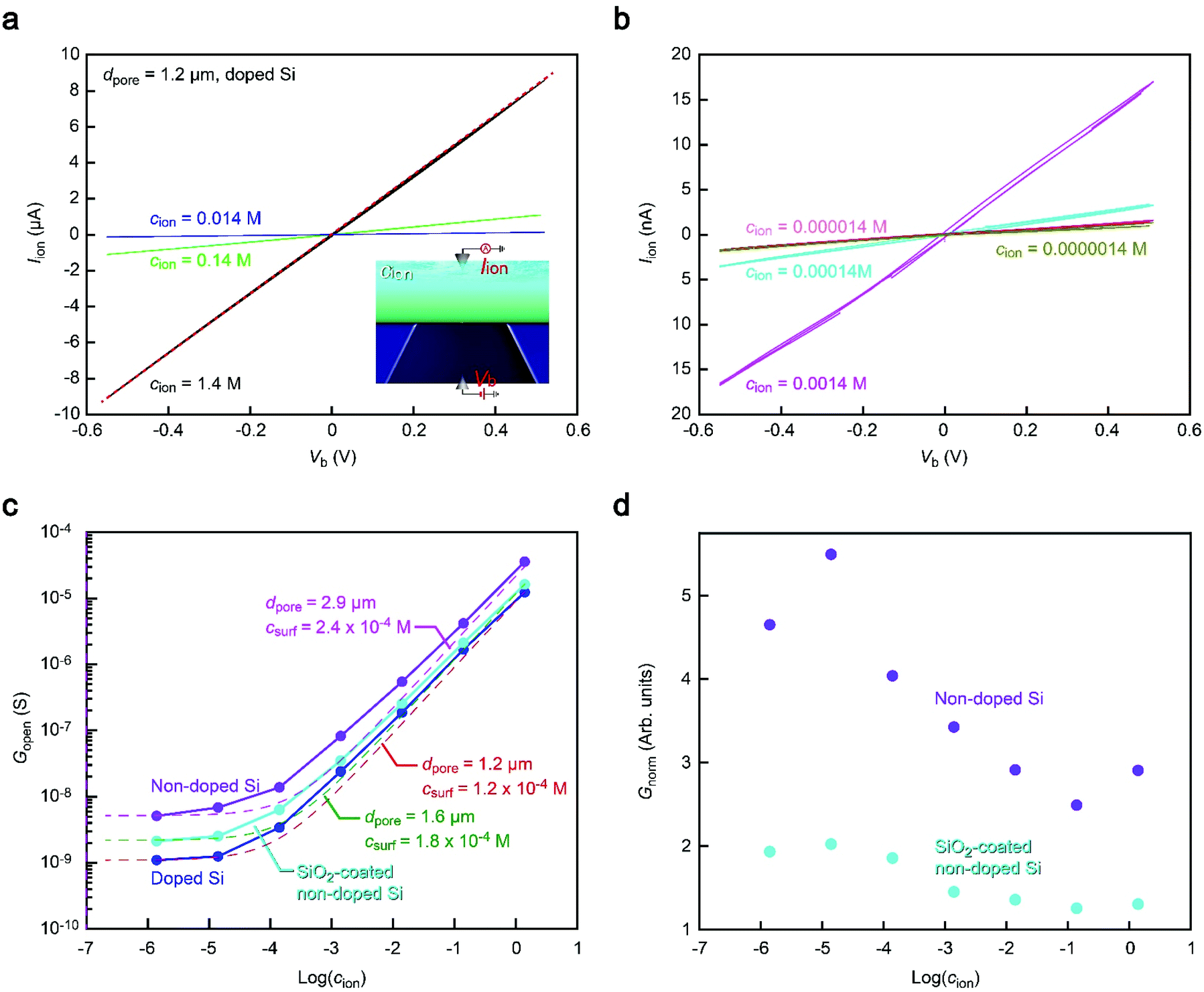 | ||
| Fig. 3 Substrate material dependence of the open pore ionic conductance. (a and b) Iionversus applied voltage Vb characteristics measured in PBS buffer of various salt concentrations cion of high (a) and low (b) ranges. Red dashed line in (a) is a linear fit to the curve at cion = 1.4 M, from which we deduced the open pore conductance Gopen. (c) Salt concentration dependence of Gopen. The dashed line is a fit presuming contributions of the ions in bulk solution cion and the surface charge on the pore wall surface csurf. Irrespective of the substrate materials, Gopen scaled linearly with the ion concentration at cion > 10−3 M. On the other hand, Gopen tended to level off at lower cion, suggesting a pronounced influence of the pore wall surface charges. (d) Gopen normalized, Gnorm, by that of doped Si plotted with respect to log(cion). | ||
Meanwhile, it is also noticeable that the conductance remains in the order (doped Si) < (SiO2-coated non-doped Si) < (non-doped Si) over the entire cion range examined (Fig. 3c), which is consistent with that shown in Fig. 2. To characterize the relative difference, we normalized Gopen by that of non-doped Si. The thus obtained Gnorm demonstrated that while the conductance ratio remains almost constant at cion > 10−2 M, the discrepancy becomes more pronounced at lower ion concentrations until it saturates at cion < 10−4 M (Fig. 3d). This rather complicated behavior suggests a difference in the size of the ion-carrying channel in the Si3N4 membrane. For example, Gnorm at the high cion regime indicates a larger amount of drift current suggestive of a larger space for the ions to traverse the membranes on the non-doped Si substrates. Although no conspicuous difference in dpore was found under a scanning electron microscope together with any signs of additional channels in the membranes, it implies that some tiny pinholes were inadvertently created in the ultrathin membranes that mutually contributed to raising Gopen for the cases of the non-doped substrates. As for the comparatively lower conductance in the nanopore on SiO2-coated Si, it can be due to the filling of the pin holes by the deposited SiO2 layer.
More quantitatively, the Gopen–cion characteristics can be compared to the aforementioned theoretical model of Gpore = σdpore, wherein we ignored the negligibly small resistance inside the pore compared to the access resistance in the present low thickness-to-diameter aspect-ratio pores. In the equation, the solution conductivity σ can be described as αcnet, where α is a constant and cnet is the concentration of ions relevant to the ionic current. Considering the role of the wall surface charges on Gopen, cnet is further approximated to be cnet = cion + csurf, where csurf is the concentration of the surface charge-induced mobile ions. Indeed, Fig. 3c can be fitted by different dpore values from 1.2 μm of the doped Si to 2.9 μm of the non-doped Si with similar csurf in the range of 10−4 M. These results corroborate a variation in the net size of ion carrying pores in the membrane. We emphasize that while there seem to be additional small channels, the pore to detect nanoparticles had a size as defined in the nanofabrication processes as confirmed by electron microscopy observations that ensures no notable difference in the resistive pulse patterns among the Si substrates used.
Blunted resistive pulses in a high-resistance pore
It therefore remains unclear why the resistive pulses became larger in the non-doped Si chips even when taking into account the experimental errors in the diameter of pores (Fig. S1†) as well as distributions in the size of nanoparticles (<5%). In this context, it is noticeable that the substrate effects on ionic blockades were found to be more pronounced in resistive channels as described below. The ionic current flowing through a pore of dpore = 1.2 μm on doped Si in 0.1× PBS was found to be 15 nA at 0.1 V (Fig. 4a and b). The corresponding Rpore of 6.7 MΩ was about a factor of 4 larger than that in the 300 nm sized nanopore in 1× PBS (Fig. 2b). In this relatively high-resistance pore, the resistive pulses (obtained for 780 nm sized carboxylated polystyrene beads) showed a marked difference in their height when changing the support material from doped Si to non-doped Si (Fig. 4c–e).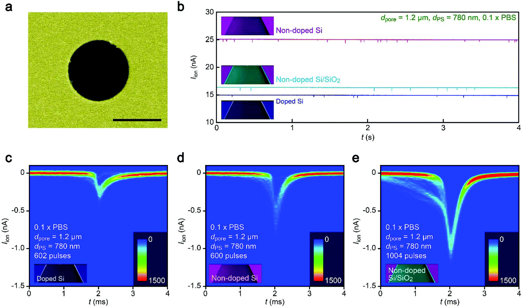 | ||
| Fig. 4 Resistive pulse analysis under low ionic conductance conditions. (a) False-colored scanning electron micrograph of a micropore of dpore = 1.2 μm in a 50 nm thick Si3N4 membrane. Scale bar denotes 1 μm. (b) Typical ionic current curves obtained with the 1.2 μm sized pore supported on a doped Si (blue), non-doped Si (purple), and SiO2-coated non-doped Si (skyblue). (c–e) Two-dimensional histograms showing a number of resistive pulses obtained with the 1.2 μm sized pore supported on a doped Si (c), non-doped Si (d), and SiO2-coated non-doped Si (e). The open pore current is offset to zero. | ||
A possible explanation for the peculiar substrate dependence of ionic current blockade is signal retardation due to the charging of capacitance in the nanopore system,18 which is described by the time constant τ = RporeCnet, where Cnet is the net capacitance of the whole chip. Indeed, the spike-like signals in the 1.2 μm sized pore can be fitted with an exponential decay function Iion = I0![[thin space (1/6-em)]](https://www.rsc.org/images/entities/char_2009.gif) exp(−t/τdecay) with a longer time constant τdecay (633 μs) for doped Si compared to the non-doped Si counterpart (288 μs) for the case of 1.2 μm sized pores (Fig. 5a–c, see also Fig. S3†). The tendency was qualitatively the same in the 300 nm sized nanopores due in part to the lower Rpore (Fig. 5d, see also Fig. S4†). This strongly suggests a prominent role of substrate-material-derived RC effects in the ionic current measurements: the resistive pulses in a pore on doped Si (non-doped Si) were significantly (less) retarded by the long (short) charging time at the capacitive components of the Si chips.
exp(−t/τdecay) with a longer time constant τdecay (633 μs) for doped Si compared to the non-doped Si counterpart (288 μs) for the case of 1.2 μm sized pores (Fig. 5a–c, see also Fig. S3†). The tendency was qualitatively the same in the 300 nm sized nanopores due in part to the lower Rpore (Fig. 5d, see also Fig. S4†). This strongly suggests a prominent role of substrate-material-derived RC effects in the ionic current measurements: the resistive pulses in a pore on doped Si (non-doped Si) were significantly (less) retarded by the long (short) charging time at the capacitive components of the Si chips.
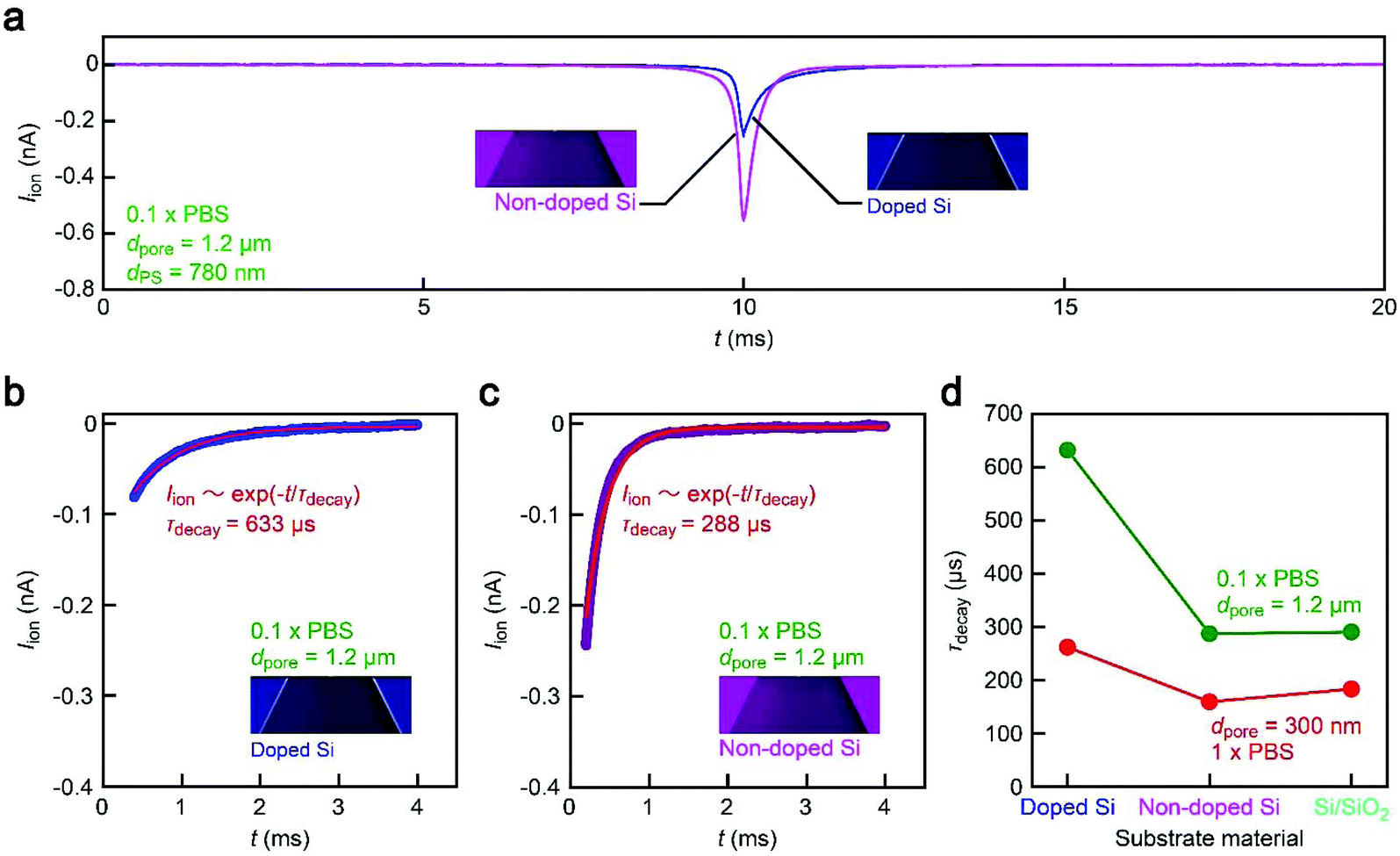 | ||
| Fig. 5 Roles of substrate materials in the temporal response of the ionic current. (a) Average resistive pulses obtained with the 1.2 μm sized pore for 780 nm sized polystyrene nanoparticles in 0.1× PBS. The open pore current is offset to zero. The pulse became significantly blunt in the nanopore on doped Si than that on non-doped Si. (b and c) Ionic current decay at the resistive pulse tails for the 1.2 μm sized pore on doped (b) and non-doped Si (c). The red curves are exponential fitting that provides the decay constant τdecay. (d) Substrate material dependence of τdecay. | ||
Substrate-capacitance-derived signal retardation in a nanopore
How exactly did the substrate contribute to the Iion response to single-nanoparticle translocation then? In the description of time constant, the first term Rpore is solely determined by buffer resistivity and nanopore geometry, both of which were arranged to be the same in the experiments (except the anomalous leakage-like current in non-doped Si chips). This is in fact evident in the Iion traces (Fig. 2a and 4b) showing a similar open pore current through the nanoscale conduit in two different substrates of doped Si and SiO2-coated non-doped Si.With Rpore being not so different, the distinct difference in the resistive pulse waveforms should be attributed to Cnet. Usually, the nanopore structure is modeled as a parallel circuit of Rpore and the cross-membrane capacitance Cnet (Fig. 6). In the present device architecture, Cnet can be modeled as serial-connected capacitors of CEDL/2, CSi3N4, and CSi denoting the capacitance of the electric double layers, the 50 nm thick Si3N4 regions, and the 525 μm thick Si support, respectively. Among the components, CEDL is appreciably larger than the others,26 and thus less important when connected in series. Whether the Si layer affects the ion blockade current therefore depends on the relative size of CSi3N4, and CSi. Based on the fact that the change in the composition of Si led to a pronounced effect on the resistive pulse patterns, CSi was anticipated to be smaller or at least comparable to CSi3N4. Indeed, from bulk physical properties, CSi3N4 and CnSi of non-doped Si per area are estimated to be 65 nF cm−2 and 0.2 nF cm−2, reflecting the two orders of magnitude difference in their thickness together with a minor influence of the relative permittivity of 11.7 and 7.3 for intrinsic Si and Si3N4, respectively. Cnet is then deduced as Cnet = CSi3N4CnSi/(CSi3N4 + CnSi) ∼ CnSi for the intrinsic Si (Fig. 6a).
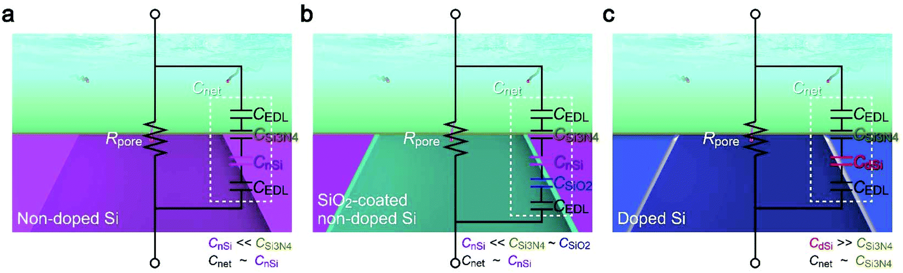 | ||
| Fig. 6 Capacitance of nanopore chips. (a–c) Equivalent circuits of a nanopore on non-doped Si (a), SiO2-coated non-doped Si (b), and doped Si (c). | ||
The discussion is the same for the case where non-doped Si is covered with 50 nm thick SiO2 as its capacitance is only comparable to that of the Si3N4 layer, and hence contributes little to Cnet due to the significantly smaller CnSi connected in series (Fig. 6b). In contrast, the high conductivity of doped Si suggests a huge dielectric constant27,28 that makes its capacitance CdSi to be excessively larger than CSi3N4, and hence Cnet ∼ CSi3N4. As a consequence, the net capacitance became much larger for the nanopore on doped Si, thereby rendering inadequate temporal resolution of the ionic current measurements for detecting the fast ion blockade events by the single-nanoparticle translocation (Fig. 6c). In fact, when assuming the real translocation time to be 287 μs, the pulses should be detected as 288 μs and 633 μs wide signals on non-doped and doped Si considering the RC delay with the relative difference in the specific capacitance, which is in fair agreement with the experimental results (Fig. 5). The overall findings can be used to achieve a faster temporal response of the ionic current and better signal-to-noise ratio in resistive pulse analyses using Si-based solid-state nanopores.
Signal retardation in smaller nanopores
It is interesting to estimate the RC effect in smaller nanopores. For this, we calculated Rnet using an access resistance model29 as Rnet = Rpore + Racc, where Rpore = Rpore = 4ρL/πdpore2 and Racc = ρ/dpore are, respectively, the resistance inside and outside the pore of diameter dpore and depth tpore = 50 nm. The solution resistivity ρ in the equation was tentatively assumed to be 0.8 Ω m for 1× PBS. Then, we deduced the time constant for the cases of Cnet = 95 pF and 0.3 pF corresponding to the properties of a 50 nm thick Si3N4 membrane on doped and non-doped 500 μm thick Si substrates, respectively. The thus obtained τdelay − dpore dependence (Fig. 7) suggested a significant influence of Rnet on nanopores smaller than 100 nm under the conditions assumed. The detrimental influence is expected to become more significant when using a thinner membrane, which is a prerequisite for sensing ultrafine particles and molecules such as proteins30 and polynucleotides.31 This predicts the importance to devote additional efforts to lower the capacitance by shrinking the water-touching area of thin dielectrics17 and also to decrease the net resistance by using an electrolyte solution with a higher ion concentration.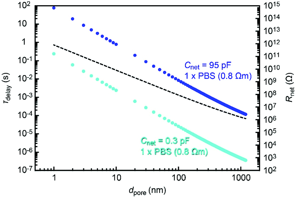 | ||
| Fig. 7 Time constant in smaller nanopores. Blue and sky blue plots are τdelay obtained for a pore of diameter dpore in a 50 nm thick Si3N4 membrane supported on doped and non-doped Si, respectively, in 1× PBS. The dashed line describes the dpore dependence of the pore resistance Rnet. | ||
Dielectric breakdown as a possible cause of pinhole generation
The variation in nanopore chip capacitance infers dielectric breakdown in a Si3N4 membrane as a cause of the anomalous cross-pore ionic current characteristics on non-doped Si. Yanagi et al.17 reported that electric charge imbalance between the two sides of a thin Si3N4 membrane would trigger a local fracture at intrinsic defects in the material in a manner akin to dielectric breakdown. The phenomenon was found to occur more easily in devices with lower capacitance due to the higher voltage induced upon injecting an electrolyte solution to a membrane.32 The resulting leakage current through the created pinholes became larger with decreasing capacitance.32 This would be a plausible explanation for the present results: the lower (higher) capacitance of the non-doped (doped) Si chips tends to trigger (hinder) dielectric breakdown yielding the larger (negligible) leakage-like ionic current through the membrane; meanwhile, SiO2 deposition on non-doped Si contributed to slightly enlarge the net capacitance, thereby partially preventing electrical breakdown. The overall findings consistently indicate the importance of the substrate material not only for achieving a high temporal resolution of nanopore sensing but also for preventing unintentional formations of nanoholes in a membrane.Conclusions
We systematically evaluated the influence of Si substrate materials on the performance of Si3N4 nanopore single-particle detectors. Although the only difference in the silicon substrate materials is the amount of impurities, and despite the fact that the substrate is located far away from the pore and so hardly imaginable to influence the cross-pore ion transport, the results demonstrated a pronounced influence on the ionic current sensitivity to single-nanoparticle translocation. Specifically, when a nanopore on a doped Si wafer was used, the relatively small capacitance at the thick silicon provided a short RC time constant with fast response of Iion to the fast electrophoretic translocation of nanoparticles through the nanoscale conduit. In the case of doped Si, in contrast, its huge capacitance eventually raised the net capacitance of the device chip compared to that on the non-doped Si, thereby causing significant retardation of resistive pulse signals. The present results prove the usefulness of highly insulating silicon as a substrate material for attaining better performance of solid-state nanopore sensors.Methods
Chemicals and materials
Si3N4-coated silicon wafers were purchased from Electronics and Materials. Carboxylated polystyrene nanoparticles were purchased from Polyscience and used without any filtering. Phosphate buffered saline (PBS) was purchased from Wako. Ultra-pure water with a resistivity of 18.2 MΩ cm was obtained using a Milli-Q Millipore system (Merck Millipore). Electron beam resist ZEP520A was purchased from Zeon.Solid-state nanopore fabrications
Solid-state nanopores were fabricated as follows. A 525 μm thick silicon wafer with 50 nm thick Si3N4 layers grown on both sides via low-pressure chemical vapor deposition was diced into 30 mm × 30 mm chips using a dicer. The Si layer was either non-doped (conductivity < 1000 Ω cm) or phosphor-doped (conductivity = 1–20 Ω cm). 1 mm × 1 mm area of Si3N4 was removed by reactive ion etching using CF4 gas. The exposed Si was then deep-etched in KOH solution heated to 80 degrees celsius. As a result, a 50 nm thick Si3N4 membrane of approximately 100 μm × 100 μm square dimension was formed at the bottom of the pyramidal-shaped trench. On the membrane, we spin-coated an electron beam resist (ZEP520A, Zeon) for electron-beam-drawing a nanopore. In the case of the non-doped Si substrate, we added a conductive spacer (ESPACER, Showa Denko) to avoid charge-up. A circle of diameter dpore was then rendered by a standard electron-beam lithography method in a membrane. After development, the remaining resist was used as a mask to drill a nanopore by isotropically etching the surface by reactive ion etching (etchant gas = CHF3). Then, the residual resist was dissolved in N,N-dimethylformamide followed by rinsing in ethanol and acetone. Before the measurements, we sealed the nanopore chip from both sides with two polymer blocks made of polydimethylsiloxane (PDMS). This was done by first activating the surface with oxygen plasma followed by attachment to the chip surface for eternal bonding. In the PDMS blocks, there was a microchannel to inject liquid into the nanopore.Ionic current measurements
Resistive pulse analyses of single nanoparticles were implemented by measuring the ionic current Iion through a nanopore of diameter dpore sculpted in a 50 nm thick Si3N4 membrane under the applied dc voltage of 0.1 V using two Ag/AgCl electrodes. One side of the membrane was filled with a dilute dispersion solution of carboxylated polystyrene beads of diameter dPS in PBS, while the other side was immersed in PBS only. The voltage created a huge electric field at the nanopore that served to electrophoretically draw the negatively charged nanobeads into the channel. As a result, Iion tended to drop rapidly as each nanoparticle passed through the conduit due to the temporal block of the in-pore ion transport. The time-course change in the ionic current was recorded at a sampling rate of 1 MHz without any filter by using a home-built current amplifier backed by a fast digitizer (NI-5922, National Instruments) using a LabVIEW program.Resistive pulse extraction
The moving open pore current was offset to zero by subtracting the linearly fitted base current in every 0.5 seconds of the Iionversus t data. Resistive pulses were then obtained by searching for local minima below a threshold level followed by extraction of 0.005 seconds of data before and after each pulse apex.Conflicts of interest
There are no conflicts to declare.Acknowledgements
A part of this work was supported by the ImPACT Program of the Council for Science, Technology, and Innovation (Cabinet Office, Government of Japan), the “Nanotechnology Platform Project (Nanotechnology Open Facilities in Osaka University)” of the Ministry of Education, Culture, Sports, Science and Technology, Japan [No: F-12-OS-0016], and the Japan Society for the Promotion of Science (JSPS) KAKENHI Grant Number 18H01846.Notes and references
- J. E. Reiner, A. Balijepalli, J. W. F. Robertson, J. Campbell, J. Suehle and J. J. Kasianowicz, Chem. Rev., 2012, 112, 6431–6451 CrossRef CAS PubMed.
- C. Dekker, Nat. Nanotechnol., 2007, 2, 209–215 CrossRef CAS PubMed.
- L. Luo, S. R. German, W.-J. Lan, D. A. Holden, T. L. Mega and H. S. White, Annu. Rev. Anal. Chem., 2014, 7, 513–535 CrossRef CAS PubMed.
- S. Howorka and Z. Siwy, Chem. Soc. Rev., 2009, 38, 2360–2384 RSC.
- D. G. Haywood, A. Saha-Shah, L. A. Baker and S. C. Jacobson, Anal. Chem., 2011, 6, 615–624 Search PubMed.
- W. H. Coulter, US patent, 2656508, 1953 Search PubMed.
- C. Y. Kong and M. Muthukumar, J. Chem. Phys., 2004, 120, 3460 CrossRef CAS PubMed.
- H. Yasaki, T. Yasui, T. Yanagida, N. Kaji, M. Kanai, K. Nagashima, T. Kawai and Y. Baba, J. Am. Chem. Soc., 2017, 139, 14137–14142 CrossRef CAS PubMed.
- E. C. Yusko, B. R. Bruhn, O. M. Eggenberger, J. Houghtaling, R. C. Rollings, N. C. Walsh, S. N. Nandivada, M. Pindrus, A. R. Hall, D. Sept, J. Li, D. S. Kalonia and M. Mayer, Nat. Nanotechnol., 2017, 12, 360–368 CrossRef CAS PubMed.
- M. Tsutsui, T. Yoshida, K. Yokota, H. Yasaki, T. Yasui, A. Arima, W. Tonomura, K. Nagashima, T. Yanagida, N. Kaji, M. Taniguchi, T. Washio, Y. Baba and T. Kawai, Sci. Rep., 2017, 7, 17371 CrossRef PubMed.
- J. W. F. Robertson, C. G. Rodrigues, V. M. Stanford, K. A. Rubinson, O. V. Krasilnikov and J. J. Kasianowicz, Proc. Natl. Acad. Sci. U. S. A., 2007, 104, 8207–8211 CrossRef CAS PubMed.
- N. Arjmandi, W. Van Roy, L. Lagae and G. Borghs, Anal. Chem., 2012, 84, 8490–8496 CrossRef CAS PubMed.
- M.-H. Lee, J.-H. Lee, H.-M. Kim, Y.-R. Kim, T.-J. Jeon, Y. E. Pak and K.-B. Kim, Microfluid. Nanofluid., 2014, 16, 123–130 CrossRef CAS.
- A. Arima, A. H. Harlisa, T. Yoshida, M. Tsutsui, M. Tanaka, K. Yokota, W. Tonomura, J. Yasuda, M. Taniguchi, T. Washio, M. Okochi and T. Kawai, J. Am. Chem. Soc., 2018, 140, 16834–16841 CrossRef CAS PubMed.
- V. Tabard-Cossa, D. Trivedi, M. Wiggin, N. N. Jetha and A. Marziali, Nanotechnology, 2007, 18, 305505 CrossRef.
- S. Shekar, D. J. Niedzwiecki, C.-C. Chien, P. Ong, D. A. Fleischer, J. Lin, J. K. Rosenstein, M. Drndic and K. L. Shepard, Nano Lett., 2016, 16, 4483–4489 CrossRef CAS PubMed.
- Y. Goto, I. Yanagi, K. Matsui, T. Yokoi and K.-I. Takeda, Sci. Rep., 2016, 6, 31324 CrossRef CAS PubMed.
- M. Tsutsui, K. Yokota, A. Arima, W. Tonomura, M. Taniguchi, T. Washio and T. Kawai, ACS Appl. Mater. Interfaces, 2018, 10, 34751–34757 CrossRef CAS PubMed.
- T. Jain, R. J. S. Guerrero, C. A. Aguilar and R. Karnik, Anal. Chem., 2013, 85, 3871–3878 CrossRef CAS PubMed.
- M.-H. Lee, A. Kumar, K.-B. Park, S.-Y. Cho, H.-M. Kim, M.-C. Lim, Y.-R. Kim and K.-B. Kim, Sci. Rep., 2014, 4, 7448 CrossRef PubMed.
- S. W. Kowalczyk, A. Y. Grosberg, Y. Rabin and C. Dekker, Nanotechnology, 2011, 22, 315101 CrossRef PubMed.
- M. Tsutsui, S. Hongo, Y. He, M. Taniguchi, N. Gemma and T. Kawai, ACS Nano, 2012, 6, 3499–3505 CrossRef CAS PubMed.
- M. Tsutsui, Y. He, K. Yokota, A. Arima, S. Hongo, M. Taniguchi, T. Washio and T. Kawai, ACS Nano, 2016, 10, 803–809 CrossRef CAS PubMed.
- W. Guan, R. Fan and M. A. Reed, Nat. Commun., 2011, 2, 506 CrossRef PubMed.
- C. Lee, L. Joly, A. Siria, A.-L. Biance, R. Fulcrand and L. Bocquet, Nano Lett., 2012, 12, 4037–4044 CrossRef CAS PubMed.
- B. Skinner, M. S. Loth and B. I. Shklovskii, Phys. Rev. Lett., 2010, 104, 128302 CrossRef PubMed.
- S. Dhar and A. H. Marshak, Solid-State Electron., 1985, 28, 763–766 CrossRef CAS.
- S. D. Ristic, Z. D. Prijic and S. Z. Mijalkovic, Phys. Status Solidi, 1995, 148, 575 CrossRef CAS.
- S. W. Kowalczyk, A. Y. Grosberg, Y. Rabin and C. Dekker, Nanotechnology, 2011, 22, 315101 CrossRef PubMed.
- J. Wilson, L. Sloman, Z. He and A. Aksimentiev, Adv. Funct. Mater., 2016, 26, 4830–4838 CrossRef CAS PubMed.
- D. B. Wells, M. Belkin, J. Comer and A. Aksimentiev, Nano Lett., 2012, 12, 4117–4123 CrossRef CAS PubMed.
- K. Matsui, I. Yanagi and K.-I. Takeda, Sci. Rep., 2015, 5, 17819 CrossRef CAS PubMed.
Footnote |
| † Electronic supplementary information (ESI) available. See DOI: 10.1039/c8nr09042d |
| This journal is © The Royal Society of Chemistry 2019 |