
High-performance sub-10 nm monolayer Bi2O2Se transistors†
Ruge
Quhe
 *a,
Junchen
Liu
a,
Jinxiong
Wu
b,
Jie
Yang
c,
Yangyang
Wang
d,
Qiuhui
Li
a,
Tianran
Li
b,
Ying
Guo
e,
Jinbo
Yang
cf,
Hailin
Peng
b,
Ming
Lei
*a and
Jing
Lu
*cf
*a,
Junchen
Liu
a,
Jinxiong
Wu
b,
Jie
Yang
c,
Yangyang
Wang
d,
Qiuhui
Li
a,
Tianran
Li
b,
Ying
Guo
e,
Jinbo
Yang
cf,
Hailin
Peng
b,
Ming
Lei
*a and
Jing
Lu
*cf
aState Key Laboratory of Information Photonics and Optical Communications and School of Science, Beijing University of Posts and Telecommunications, Beijing 100876, P. R. China. E-mail: mlei@bupt.edu.cn; quheruge@bupt.edu.cn
bCenter for Nanochemistry, Beijing National Laboratory for Molecular Sciences (BNLMS), College of Chemistry and Molecular Engineering, Peking University, Beijing 100871, P. R. China
cState Key Laboratory for Mesoscopic Physics and Department of Physics, Peking University, Beijing 100871, P. R. China. E-mail: jinglu@pku.edu.cn
dNanophotonics and Optoelectronics Research Center, Qian Xuesen Laboratory of Space Technology, China Academy of Space Technology, Beijing 100094, P. R. China
eSchool of Physics and Telecommunication Engineering and Shaanxi Key Laboratory of Catalysis, Shaanxi University of Technology, Hanzhong 723001, P. R. China
fCollaborative Innovation Center of Quantum Matter, Beijing 100871, P. R. China
First published on 3rd December 2018
Abstract
A successful two-dimensional (2D) semiconductor successor of silicon for high-performance logic in the post-silicon era should have both excellent performance and air stability. However, air-stable 2D semiconductors with high performance were quite elusive until the air-stable Bi2O2Se with high electron mobility was fabricated very recently (J. Wu, H. Yuan, M. Meng, C. Chen, Y. Sun, Z. Chen, W. Dang, C. Tan, Y. Liu, J. Yin, Y. Zhou, S. Huang, H. Q. Xu, Y. Cui, H. Y. Hwang, Z. Liu, Y. Chen, B. Yan and H. Peng, Nat. Nanotechnol., 2017, 12, 530). Herein, we predict the performance limit of the monolayer (ML) Bi2O2Se metal oxide semiconductor field-effect transistors (MOSFETs) by using ab initio quantum transport simulation at the sub-10 nm gate length. The on-current, delay time, and power-delay product of the optimized n- and p-type ML Bi2O2Se MOSFETs can reach or nearly reach the high performance requirements of the International Technology Roadmap for Semiconductors (ITRS) until the gate lengths are scaled down to 2 and 3 nm, respectively. The large on-currents of the n- and p-type ML Bi2O2Se MOSFETs are attributed to either the large effective carrier velocity (n-type) or the large density of states near the valence band maximum and special shape of the band structure (p-type). A new avenue is thus opened for the continuation of Moore's law down to 2–3 nm by utilizing ML Bi2O2Se as the channel.
Introduction
As silicon technology approaches its physical limit, the identification of a new channel material could provide a pathway toward the continued scaling of complementary metal–oxide–semiconductor (CMOS) technology in the next few decades.1,2 Two-dimensional (2D) semiconducting materials emerge as promising channel material candidates, mainly because of their ideal gate electrostatics, dangling-bond-free surfaces, and uniform thicknesses.3,4 In addition to a proper band gap (preferably greater than 0.4 eV (ref. 5)), a successful 2D semiconductor successor of silicon for high performance (HP) electronics should probably meet two criteria: (1) a high drive current, which often requires a high carrier mobility; and (2) a high ambient stability. Unfortunately, 2D semiconductors that meet the two criteria have been quite elusive. With the moderate band gaps, 2D MoS2 and phosphorene are among the most intensively studied materials for electronics.6–8 2D MoS2 is the first 2D semiconductor that has been fabricated into field effect transistors (FETs) in the sub-10 nm regime.9–11 However, the experimental low on-currents (less than 250 μA μm−1),9–11 probably due to the relatively low carrier mobility, render 2D MoS2 more suitable for low power (LP) applications than HP applications. Theoretically, in terms of ab initio quantum transport simulation, the on-currents of the sub-10 nm MoS2 transistors even in extremely optimistic conditions (absence of defects, ideal geometry, and ballistic transport) also fail to meet the International Technology Roadmap for Semiconductors (ITRS) requirements12 for HP application in the next decades.13 Phosphorene and emerging 2D InSe have high carrier mobility, but their poor stability leads to rapid device performance degradation when exposed to air.14,15 Therefore, the identification of a 2D semiconductor with a proper band gap, high carrier mobility, and ambient stability is critical for post-silicon HP electronics.Recently, atomically thin 2D Bi2O2Se has been successfully synthesized by chemical vapor deposition (CVD) on a mica substrate.16,17 The Bi2O2Se crystal is a semiconductor with a layer dependent band gap of 0.31–1.14 eV at the generalized gradient approximation (GGA) level. The electron mobility of the 2D Bi2O2Se is as high as 450 cm2 V−1 s−1 at room temperature and 29![[thin space (1/6-em)]](https://www.rsc.org/images/entities/char_2009.gif) 000 cm2 V−1 s−1 at 1.9 K.16 Moreover, 2D Bi2O2Se shows excellent stability against oxidation and moisture in air. These features make 2D Bi2O2Se very attractive for the next generation electronics. The fabricated top-gated FETs with 21 μm-long Bi2O2Se channels exhibit large on/off current ratios of up to 106 and near-ideal subthreshold swing values down to 65 mV dec−1 at room temperature.16 Three fundamental questions arise naturally: (1) What is the device performance limit of 2D Bi2O2Se based FETs? (2) How does this device performance compare with that of other 2D semiconductor FETs? (3) Can 2D Bi2O2Se FETs meet the HP device requirement of ITRS?
000 cm2 V−1 s−1 at 1.9 K.16 Moreover, 2D Bi2O2Se shows excellent stability against oxidation and moisture in air. These features make 2D Bi2O2Se very attractive for the next generation electronics. The fabricated top-gated FETs with 21 μm-long Bi2O2Se channels exhibit large on/off current ratios of up to 106 and near-ideal subthreshold swing values down to 65 mV dec−1 at room temperature.16 Three fundamental questions arise naturally: (1) What is the device performance limit of 2D Bi2O2Se based FETs? (2) How does this device performance compare with that of other 2D semiconductor FETs? (3) Can 2D Bi2O2Se FETs meet the HP device requirement of ITRS?
In this paper, we investigate for the first time the performance limit of the n- and p-type sub-10 nm double-gated (DG) monolayer (ML) Bi2O2Se metal–oxide semiconductor FETs (MOSFETs) using accurate ab initio quantum transport simulations. The on-currents of the sub-10 nm ML Bi2O2Se MOSFETs are much larger than those of their ML MoS2 counterparts across most of the size range tested. The optimized n- and p-type DG ML Bi2O2Se transistors can reach or nearly reach the ITRS goals for the on-state current, delay time and power-delay product (PDP) of the HP devices until the gate lengths are scaled down to 2 nm and 3 nm, respectively. On the basis of the available data, we reveal that either a very small or a very large effective electron (hole) mass favors a large on-state current for the 2D semiconductor FETs.
Results
ML Bi2O2Se is modeled by buckled [Bi2O2] layers in the middle with planar Se layers terminating both the top and bottom surfaces, to keep the bulk inversion symmetry (Fig. 1(a)).16 The outermost Se layers are passivated by H atoms in accordance with the previous study.16 The optimized lattice parameter of the Bi2O2Se monolayer is 4.03 Å, in agreement with other theoretical calculations.18 The band structure of the ML Bi2O2Se with H atom termination is shown in Fig. 1(b), and an indirect band gap of 1.14 eV is observed with a conduction band minimum (CBM) and valence band maximum (VBM) located at the Γ and X points, respectively. The band near the CBM is quite steep, leading to a very small effective mass of 0.20m0 for the electrons. On the contrary, the band near the VBM is relatively flat, leading to a large effective mass of 1.40m0 for holes. From the projected density of states, the states near the CBM mainly originate from the Bi atoms, while the states near the VBM are from the Se atoms.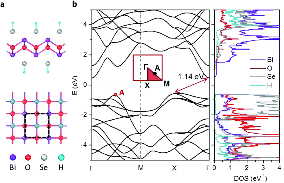 | ||
| Fig. 1 Crystal and electronic structures of ML Bi2O2Se. (a) Side and top views of ML Bi2O2Se. The dashed rectangle indicates the primitive unit cell. (b) Band structure and projected density of states. The inset shows the first Brillouin Zone. | ||
A gated two-probe model of the DG ML Bi2O2Se MOSFET is constructed with intrinsic ML Bi2O2Se as the channel and degenerately doped ML Bi2O2Se as the electrodes, as shown in Fig. 2(a). The underlap (UL) configuration, i.e. the spacer region between the gate and electrode, has also been considered to improve the device performance.19–22 We apply silicon dioxide as the dielectric material. The equivalent oxide thicknesses (tox) in the MOSFETs are set to 0.41–0.54 nm according to the ITRS 2.0 2013 edition requirement.
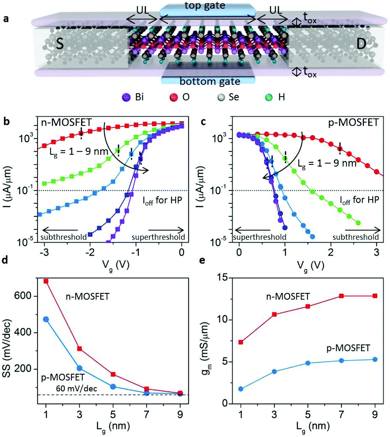 | ||
| Fig. 2 (a–c) Schematic model (a) and transfer characteristics (b,c) of the DG ML Bi2O2Se MOSFETs with gate lengths of 1 to 9 nm. (d, e) Subthreshold swing (d) and gate conductance (e) of the sub-10 nm ML Bi2O2Se MOSFETs as a function of the gate length. The supply voltage is 0.64 V and UL = 0 nm in (b–e). The arrows in (b,c) indicate the change of gate length from 1 to 9 nm with a step size of 2 nm. The vertical dashed lines in (b,c) separate the subthreshold and superthreshold regions. | ||
We first investigate the device performance without the UL configuration and with the electron/hole concentration of ρ = 5 × 1013 cm−2 in both the source and the drain. This level of doping concentration has commonly been applied in the previous 2D materials-based device simulations.23–27 Experimentally, the doping strategy for 2D layered materials includes substitutional doping,28,29 ion implantation,30,31 plasma treatment,32 surface charge transfer,33 and photoinduced doping.34 With the introduction of AuCl3 dopants, a p-type doped MX2 transistor with a hole concentration of 5 × 1013 cm−2 is achieved.35 By Nb atom substitution28 or UV photoinduced doping,34 a hole or electron concentration (about 1014 cm−2) that is even higher than our modeled value is achieved in MoS2. Theoretically, we model the effect of doping by changing the number of electrons of the system with respect to the neutral case. Correspondingly, the electrostatic potential acting on the Kohn–Sham one-electron states is modified.
The transfer characteristics of the Bi2O2Se n- and p-MOSFETs at a supply voltage Vdd = 0.64–0.72 V are shown in Fig. 2(b) and (c). At a given gate voltage Vg, the currents of the n-MOSFETs are generally higher than those of the p-MOSFETs due to the smaller effective mass (me = 0.20m0vs. mh = 1.40m0) and thus higher carrier mobility of electrons than holes. As the gate length Lg decreases, the current increases apparently in the subthreshold region, a result associated with the more severe source to drain direct tunneling.
From the transfer characteristics, we extract the subthreshold swing (SS) and transconductance (gm) values to evaluate the gate control ability in the ML Bi2O2Se MOSFETs in the subthreshold and superthreshold regions, respectively. A small SS value implies weak short-channel effects, and the smallest SS achievable in thermionic devices at room temperature is 60 mV dec−1. As shown in Fig. 2(d), the SS values of n- and p-MOSFETs show similar degradation behavior at shorter Lg, and the former degrade faster. At Lg = 9 nm, the nearly ideal SS value of 60 mV dec−1 is achieved in both the n- and p-MOSFETs. As Lg decreases to 1 nm, the SS values increase to 600 and 500 mV dec−1 in the n- and p-MOSFETs, respectively. The trend to larger SS values at shorter Lg is consistent with the stronger gate controllability at the band edge location (Fig. S1†). The gate control ability in the superthreshold region also decreases with the shorter Lg, as evidenced by the smaller gm values (Fig. 2(e)). Notably, the ML Bi2O2Se n-MOSFETs show generally larger gm values (7–12 mS μm−1) than the p-MOSFETs (2–5 mS μm−1), implying a better superthreshold gate control for the former over the latter.
In a digital device, a higher on–state current is beneficial for achieving a faster logic transition speed. The off–current is fixed to 0.1 μA μm−1 according to the ITRS 2.0 2013 edition standards for HP applications, and the on-current is evaluated under a supply voltage (Vdd = Vb) of 0.64–0.72 V (Table S1†). As shown in Fig. 4(a), the on-currents of the n- and p-MOSFETs without a UL fulfill the ITRS HP requirements of 900–1350 μA μm−1 until Lg = 7 nm and 5 nm, respectively. Remarkably, the on-current in the Bi2O2Se n-MOSFET at Lg = 9 nm reaches 3500 μA μm−1. This on-current is the highest among the simulated sub-10 nm transistors based on the stable 2D semiconductors at the ab initio quantum transport level, to the best of our knowledge.13,19,26
To further improve the device performance, utilization of the UL structure is a viable solution. The UL could improve the subthreshold electrostatics because it increases the effective channel length and thereby suppresses the source to drain leakage. We consider the symmetric UL structure in the ML Bi2O2Se MOSFETs with Lg ≤ 5 nm; the length of the UL is chosen under the precondition of keeping the whole channel length (Lch = Lg + 2 × UL) at less than 10 nm. As shown in Fig. S2,† the transfer characteristics of the 1 nm-gate-length n- and p-MOSFETs become steeper in the subthreshold region with the increasing UL. As the UL increases from 0 to 4 nm, the SS values decrease from 660 to 168 mV dec−1 and from 474 to 111 mV dec−1 for the 1 nm-gate-length n- and p-MOSFETs, respectively. This enhanced electrostatic effect by the UL also occurs in all the other studied cases. As shown in Fig. S3(a and b),† the longer UL always renders a smaller SS. The SS decreases by 28–75% with the aid of the UL, and the magnitude of the SS reduction is larger for devices with shorter Lg.
The improved gate control in the subthreshold region by using the UL is also reflected in the enhanced modulation of the band edge location by Vg. Take the ML Bi2O2Se p-MOSFET at Lg = 1 nm as an example. In Fig. 3, we define a maximum hole barrier height ϕmax as the energy barrier for the holes at the VBM of the source (E = −0.32 eV) to transport to the drain. To keep the same off-current of 0.1 μA μm−1 in the off-state, ϕmax is largest at UL = 0 nm followed by UL = 2 nm and UL = 4 nm (Fig. 3(a)–(c), respectively), and the peaks of the three spectral current curves are of the same order of magnitude (Fig. 3(d)). Under the gate modulation of 0.64 eV, the VBMs of the ML Bi2O2Se MOSFETs in the channel move upward, and the devices are turned to the on-state. ϕmax decreases slightly by 0.10 eV at UL = 0 nm, while it decreases significantly by 0.31 eV at UL = 2 nm and by 0.25 eV at UL = 4 nm (Fig. 3(e)–(g)). The enhanced subthreshold electrostatics induced by the UL are advantageous for boosting the on-current. As shown in Fig. 3(h), the peak of the spectral current increases apparently with the longer UL. Remarkably, the current chiefly comes from those transmissions with the energy below the chemical potential of the source μs (namely out of the bias window) in terms of the spectral current. The maximum enhancement of the on-current by the UL is 21 times in the ML Bi2O2Se MOSFET with Lg ≤ 5 nm (Fig. S3(c and d)†). After applying the UL, the on-currents of the ML Bi2O2Se p-MOSFET at Lg = 3 nm and n-MOSFET at Lg = 2 nm reach 1127 and 871 μA μm−1, respectively, fulfilling or almost fulfilling the ITRS requirement of 900 μA μm−1 (Fig. 4(a)).
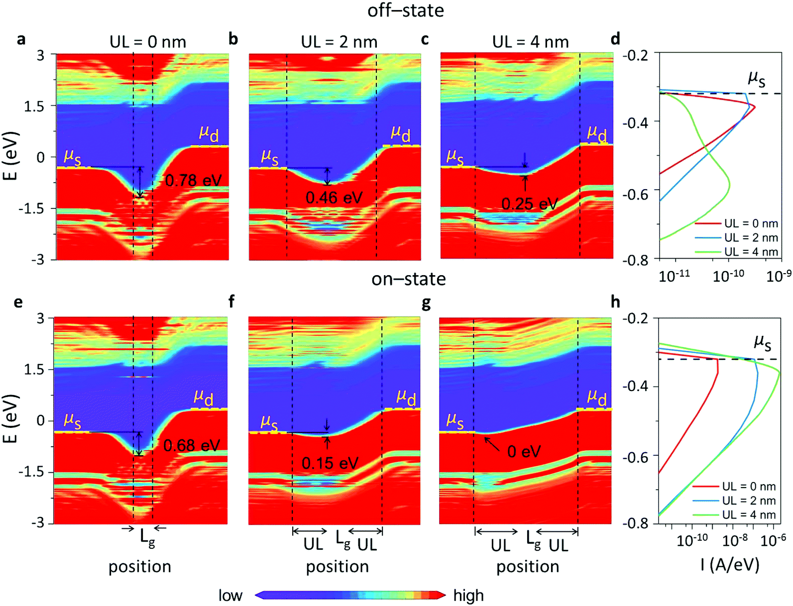 | ||
Fig. 3 Comparison of the local density of states (a–c, e–g) and spectral currents (d,h) of the ML Bi2O2Se p-MOSFETs at the off- and on-states with different ULs. Lg = 1 nm; μs and μd are the electrochemical potential of the source and the drain, respectively. The off-state has a current of 0.1 μA μm−1, and the on-state is the state with a gate difference of Vdd = 0.64 V to the off-state. The maximum hole barrier height ϕmax is labeled. The spectral current is defined as 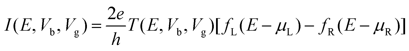 . . | ||
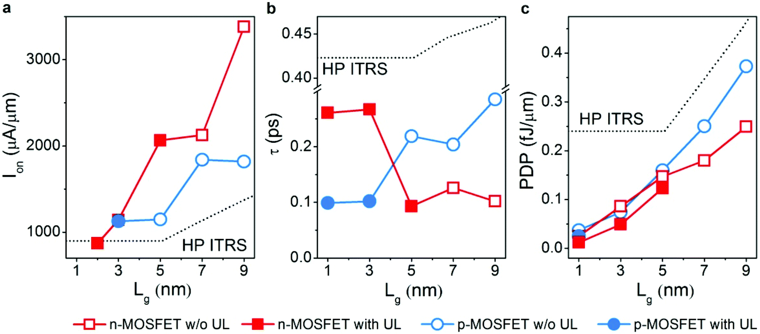 | ||
| Fig. 4 Benchmark of the on-state current, intrinsic delay time, and power-delay product of the sub-10 nm ML Bi2O2Se MOSFETs against the ITRS 2013 edition requirements for HP applications. The supply voltage is 0.64–0.72 V. Only the devices whose performances fulfill or almost fulfill the requirements are shown. The red and blue colors indicate the n-MOSFET and p-MOSFET, respectively, and the solid and empty circles indicate the MOSFETs without a UL and with the optimal UL, respectively. | ||
Next, we check the intrinsic gate delay time (τ) and PDP, which are two key figures of merit reflecting the switching speed and power efficiency for the transistor operation, respectively. The fringing capacitance Cf is included by assuming it is twice the intrinsic gate capacitance Cg according to the ITRS requirements. The total capacitance Ctotal is the sum of Cg and Cf. The delay time is calculated by τ = CtotalCdd/Ion. Without the UL, the calculated delay times (0.10–42.00 ps) of the ML Bi2O2Se n- and p-MOSFETs meet the ITRS HP requirements of 0.423–0.446 ps until Lg = 7 nm and 5 nm, respectively (Fig. 4(b)). The introduction of the UL brings τ of the ML Bi2O2Se n- and p-MOSFETs below 0.26 ps at Lg ≤ 5 nm, thus meeting the ITRS HP goal even at Lg = 1 nm. PDP is calculated according to the equation PDP = VddIonτ = CtotalVdd.2 Even without the UL, PDPs of the sub-10 nm ML Bi2O2Se n- and p-MOSFETs range from 0.03 to 0.37 fJ μm−1 and decrease with shorter Lg values (Fig. 4(c)). The use of the optimal UL makes PDP decrease by 20%–110% in the ML Bi2O2Se MOSFETs at Lg < 5 nm. Therefore, the sub-10 nm ML Bi2O2Se n- and p-MOSFETs require low energy during on–off state switching, in terms of the smaller PDP compared with the ITRS requirements for HP application (0.24–0.45 fJ μm−1).
We have also explored the potential of the sub-10 nm ML Bi2O2Se n- and p-MOSFETs for LP application. The details are provided in Table S2 and Fig. S4.† For the n-MOSFETs, the leakage current is too large to be lower than the ITRS off-current requirement of 10−5 μA μm−1, due to the small effective mass and short channel barrier. For the p-MOSFETs, only those with 7- and 9 nm gate lengths could fulfill the ITRS LP requirements for the on-current and the application of a UL does not help. Apparently, ML Bi2O2Se is less satisfactory for LP applications in the sub-10 nm region.
Discussions
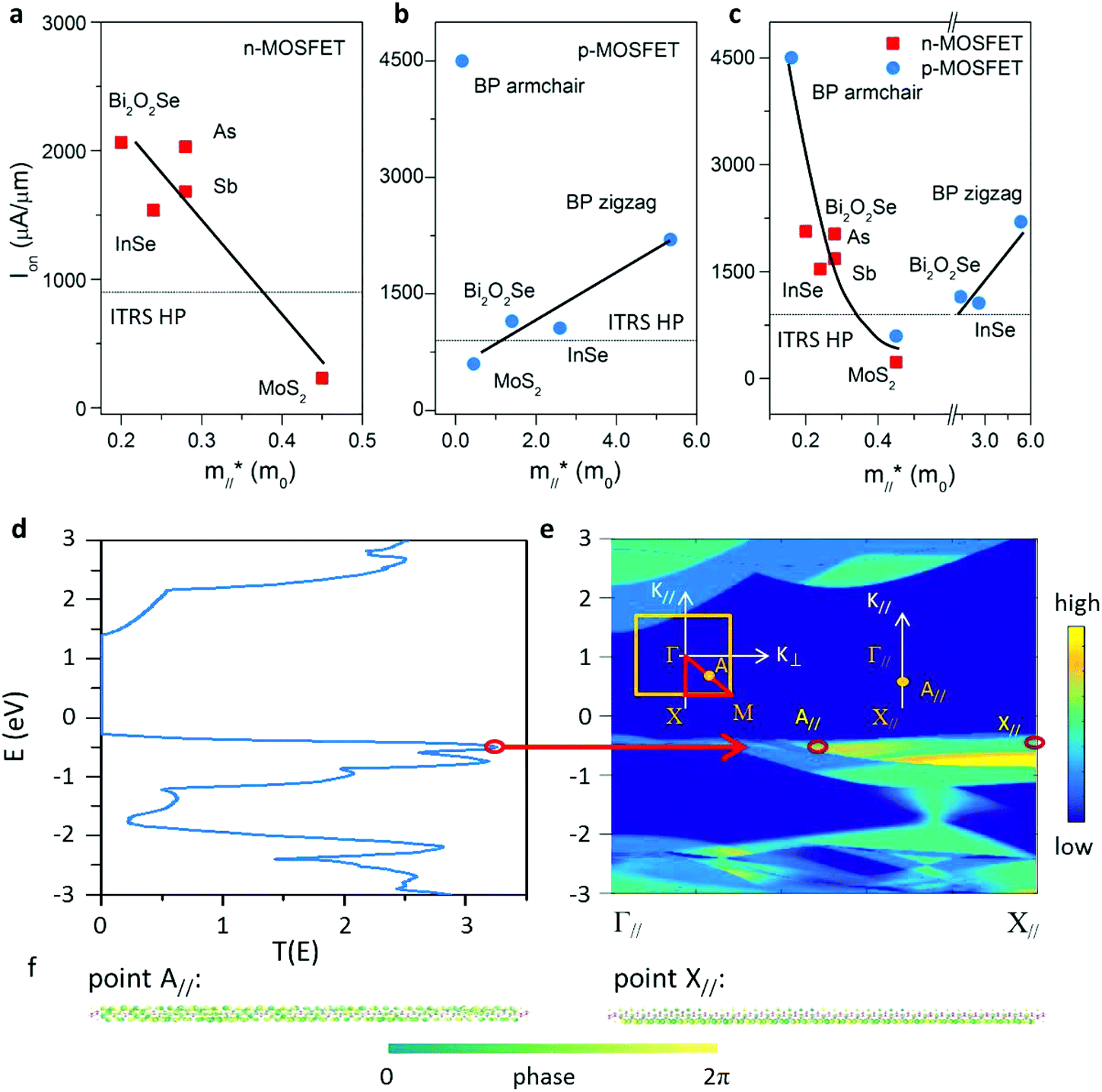
It is intriguing to compare the on-currents of the sub-10 nm ML Bi2O2Se MOSFETs with those of other typical 2D semiconductor MOSFETs, such as ML phosphorene,21,36 arsenene,19,26 antimonene,19,26 InSe,20 and MoS2 MOSFETs. Fig. 5 shows the highest reported on-currents of the MOSFETs so far calculated at the ab initio quantum transport level. The UL configuration has been considered in this comparison. The p-type ML phosphorene MOSFETs and n-type ML arsenene/antimonene MOSFETs generally show higher or similar overall on-currents compared with those based on ML Bi2O2Se. However, the stability issues of phosphorene37 and arsenene remain a major obstacle. The possible formation of highly toxic arsenic trioxide in the fabrication of 2D arsenene is another concern.38 ML antimonene is air stable,38 but ML antimonene transistors with high performance have not been fabricated yet. Compared with the ML InSe MOSFETs, the n-type ML Bi2O2Se MOSFETs have superior on-current at Lg ≥ 5 nm and the p-type ML Bi2O2Se MOSFETs are superior at Lg ≥ 3 nm but they give worse or similar performance at small gate lengths (Lg < 5 nm for the n-type MOSFETs and Lg < 3 nm for the p-type MOSFETs). However, spontaneous surface oxidation of InSe in ambient conditions is harmful for mobility and degrades the device performance greatly.15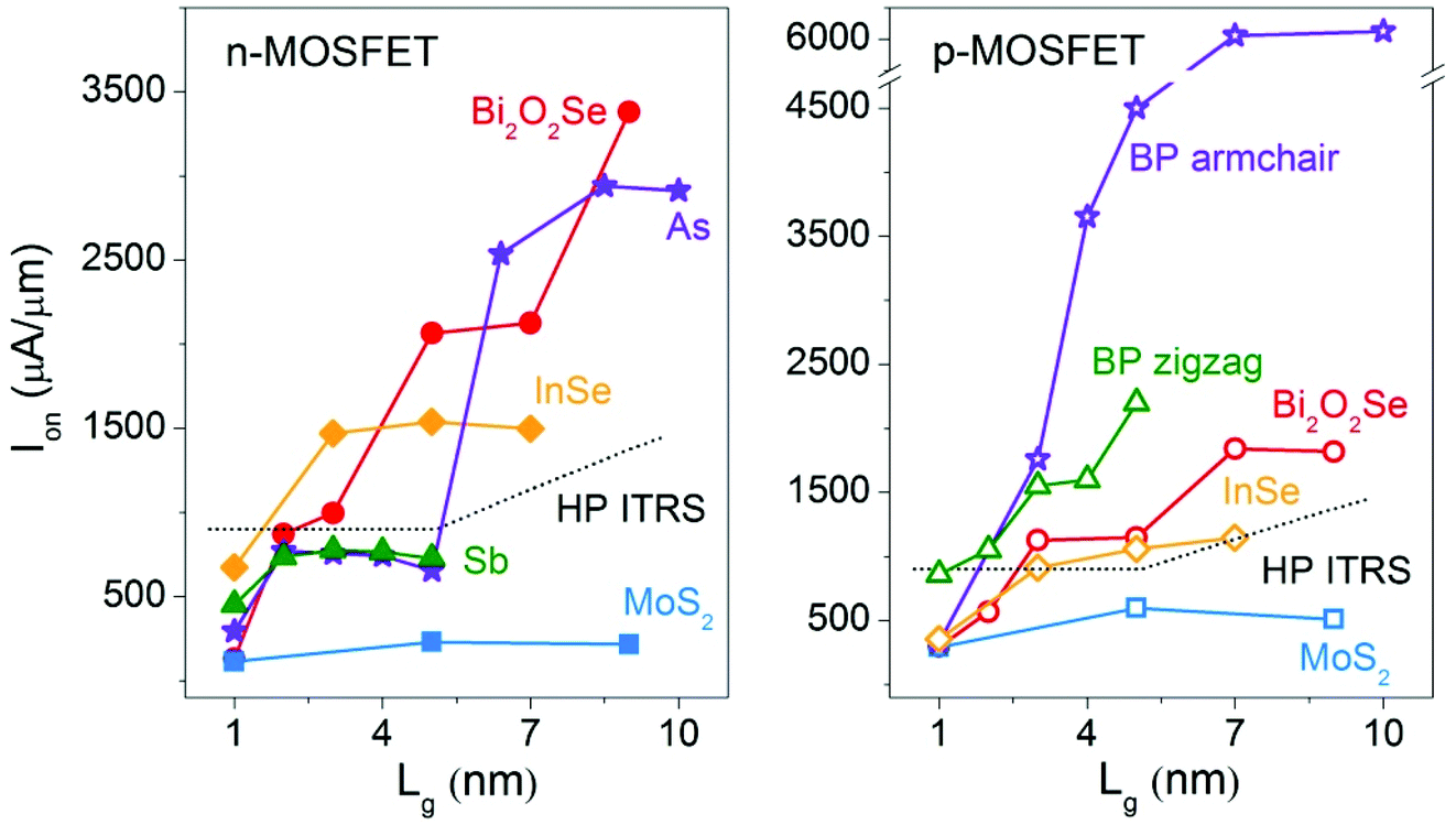 | ||
| Fig. 5 Comparison of the on-currents of the optimal ML Bi2O2Se, black phosphorus (BP),21,36 arsenene (As),19,26 antimonene (Sb),19,26 InSe,20 and MoS2 MOSFETs at different gate lengths obtained from the ab initio quantum transport simulations. The presented on-current has been optimized by using a UL. The detailed computational parameters are provided in Table S4.† | ||
Remarkably, the on-currents of the ML Bi2O2Se MOSFETs exceed those of the ML MoS2 ones, and the difference increases with increasing Lg. At Lg = 9 nm, the on-currents of the ML Bi2O2Se n- and p-MOSFETs are 15.6 and 3.6 times, respectively, those of their ML MoS2 counterparts. Besides the on-state current, the sub-10 nm ML Bi2O2Se MOSFETs also show generally superior performance to ML MoS2 in terms of the delay time and PDP (Table S3†). We are aware that the recently fabricated semiconductor tellurene (2D tellurium) also possesses both high carrier mobility and air stability,39 but its performance limit is unclear.
To interpret the difference in the on-current of the above 2D material-based transistors, it is helpful to check the dependence of the on-current on the effective mass of the channel materials along the transport direction ( ). A small effective mass of the channel material produces two effects: (1) it implies a large carrier effective velocity along the transport direction, which is beneficial for achieving a large on-current. (2) It implies a small density of states (DOS) near the VBM or CBM (
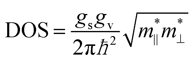 , where the symbols ‖ and ⊥ indicate the transport and transverse directions, respectively). This is a disadvantage for achieving a large on-current, because a small DOS near the VBM or CBM indicates that a large variation of the gate voltage ΔVg is needed to drive a certain variation of the channel charge ΔQch, leading to a small transconductance gm. Another disadvantage, namely large tunneling leakage induced by a small
  , is not discussed here as this has been depressed by the aid of the UL.
In Fig. 6(a) and (b), we provide the on-current as a function of the effective mass in the 2D semiconductor n- and p-MOSFETs, respectively, with Lg fixed at 5 nm. In the range of small effective masses 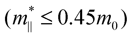 , the on-current shows an increasing trend with decreasing m* for both the n- and p-MOSFETs. In the range of large effective masses
 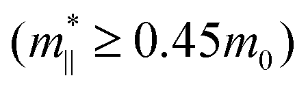 , the on-current shows an increasing trend with increasing
  for the p-MOSFETs. The relation between
  and on-current (Ion) in the n- and p-MOSFETs can be well fitted by the linear functions
 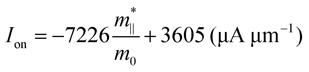 and
and 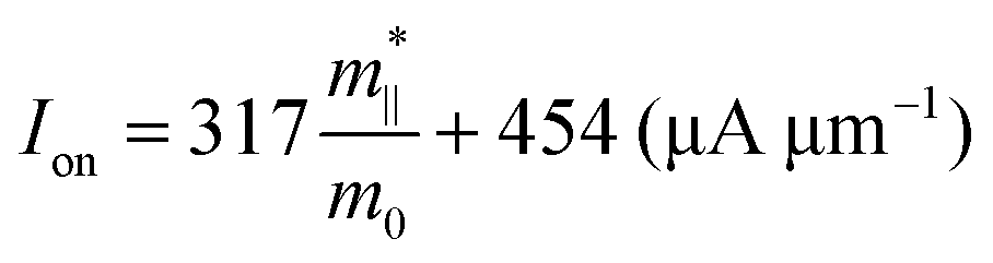 , respectively (except for the armchair-directed ML phosphorene p-MOSFET).
 | ||
| Fig. 6 (a–c) On-currents of the n-MOSFET, p-MOSFET, and both n- and p-MOSFETs versus the effective masses of the ML channel material along the transport direction at Lg = 5 nm.19–21,26,36 All the data here are obtained from ab initio quantum transport simulations. The solid lines in (a,b) are linear fitted to the data (excluding BP in (b)). The solid line in (c) is for guidance to the eyes. (d–f) Total transmission spectra, k-point resolved transmission spectra, and transmission eigenstates of the ML Bi2O2Se p-MOSFET at the on-state. Lg = 9 nm and UL = 0 nm. The inset in (e) shows the 2D Brillouin zone of ML Bi2O2Se and the 1D Brillouin zone of the transistor. In (f), E = −0.5 eV. | ||
To establish an overall picture, we replot the data in Fig. 6(a) and (b) as a whole in Fig. 6(c). Among all the 2D semiconductors in Fig. 6(c), ML phosphorene is anisotropic  while the other channel materials are isotropic
  . For the armchair-directed ML phosphorene p-MOSFETs, the noticeably large on-current (4500 μA μm−1) comes from the fact that it possesses both a small
  and large
  at the same time. Thereby, it can achieve both a large carrier effective velocity and a large DOS near the VBM. For the other cases, the two effects introduced by the effective masses are always in opposition, and the effective mass needs to be optimized so that a balance between the two effects is established. Compared with the case of MoS2
 , ML Bi2O2Se, InSe, arsenene, and antimonene n-MOSFETs
 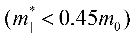 give full play to the advantage of the large carrier effective velocity while ML Bi2O2Se, InSe and phosphorene p-MOSFETs
 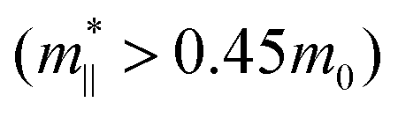 maximize the advantage of the large DOS in the on-current. Therefore, not only those 2D semiconductors with very small
  but those with large
  are worthy of exploration for ultra-scaled electronics. The ML MoS2 MOSFET with
  shows the lowest Ion in Fig. 6(c). However, more studies are needed to precisely locate the Ion minimum point since no data is available in the range of 0.45m0–1.40m0. Another question that needs more exploration is to what extent the increasing trend of the on-current at
  continues.
It is noteworthy that the special shape of the valence band of ML Bi2O2Se contributes to the large on-current in the ML Bi2O2Se p-MOSFETs. In the valence band, there is a local maximum at point A with an energy of about 0.1 eV lower than that of the VBM at the point X (Fig. 1(a)). The hole effective mass of ML Bi2O2Se at the point A is 0.21m0, only 15% of the hole effective mass at the VBM (1.40m0). The key role of the point A in the transport properties of ML Bi2O2Se can be found by checking its contribution to the on-state transmission of the device.
Fig. 6(d) and (e) shows the on-state transmission spectrum and the k-point resolved transmission spectrum of the 9 nm ML Bi2O2Se p-MOSFET. The left inset in Fig. 6(e) shows the 2D Brillouin zone of ML Bi2O2Se, and the right inset shows the 1D Brillouin zone of the device, with K‖ indicating the transverse direction. Point A‖ is the projection of the point A to the 1D Brillouin zone. The transmission peak closest to the Fermi level is located at E = −0.5 eV, and the corresponding largest transmission contribution is from the point A‖, as shown in the k-point resolved transmission spectrum. The significant contribution of A‖ to the transmission can also be found in the transmission eigenstates (Fig. 6(f)). At E = −0.5 eV, the incoming wave function of both the points A‖ and X‖ spread over the whole transistor. The wave function of the point A‖ covers both the Bi and Se atoms, while the wave function of the point X‖ is mainly localized near the Se atoms. This is related to the fact that both the orbitals of the Bi and Se atoms contribute to the point A while only the orbitals of the Se atoms contribute to the point X in the band structure (Fig. S5†).
The excellent performance of the ML Bi2O2Se MOSFETs is predicted in the Ohmic contact limit, which is ensured by the degenerately doped source and drain. Experimentally, it is rather challenging to heavily dope the 2D semiconductors,3 and the metal is often applied as the source and drain electrodes in the devices. This metal-contacted FET is termed a Schottky barrier FET (SBFET). A Schottky barrier might exist at the metal-ML Bi2O2Se interfaces and hinder the carrier injections. To achieve the predicted excellent performance in practice, it is essential to find a proper metal electrode that forms a barrier-free Ohmic contact with ML Bi2O2Se. The ab initio simulations reveal that Pt, Sc and Ti electrodes would form a desirable n-type Ohmic contact with ML Bi2O2Se.40 With these metals as electrodes, the ML Bi2O2Se SBFETs are highly likely to approach the predicted performance limit of the corresponding MOSFETs.
Conclusion
Stimulated by the recent experimental fabrication of air-stable 2D Bi2O2Se FETs with high electron mobility, we predict the performance limit of the sub-10 nm ML Bi2O2Se n- and p-MOSFETs based on rigid ab initio quantum transport simulations. The sub-10 nm ML Bi2O2Se MOSFETs show on-currents lower than those of the air-unstable ML phosphorene MOSFETs, and similar to those of the air-unstable ML InSe MOSFETs, but significantly higher than those of the air-stable ML MoS2 MOSFETs. The on-currents, delay times, and power-delay products of the optimized n- and p-type ML Bi2O2Se MOSFETs can fulfill or nearly fulfill the ITRS requirements for HP devices until the gate lengths are scaled down to 2 and 3 nm, respectively. The simultaneous possession of excellent device performance and high ambient stability renders the sub-10 nm ML Bi2O2Se MOSFETs superior to other existing 2D semiconductor counterparts as a post-silicon-era candidate channel material. Based on the analysis of a variety of ML 2D semiconductor FETs, we find that either a very small or a very large effective electron (hole) mass is beneficial for a large on-current.Computational method
The transport properties are studied based on density functional theory (DFT) combined with the nonequilibrium Green's function (NEGF) formalism, as implemented in the Atomistix ToolKit package.41 Following the Landauer–Bűttiker formula, the drain current at a given bias voltage Vb and gate voltage Vg is calculated by the equation below:42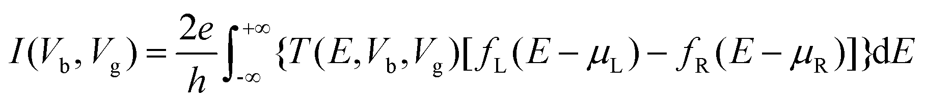 | (1) |
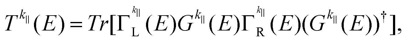
The transmission coefficient T(E) is the average of k-dependent transmission coefficients Tk‖(E) over the Brillouin zone. The k-dependent transmission coefficient at energy E is
 | (2) |
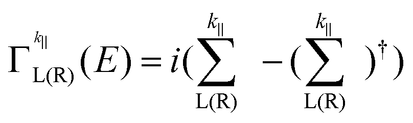 is the level broadening originating from the left (right) electrode expressed by the electrode self-energy
 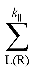 .43,44
The electrostatics are treated by solving the Poisson equation self-consistently via a real space solver. The periodic and Neumann conditions are used on the boundaries along the transverse direction and the direction normal to the Bi2O2Se surface, respectively. To make sure of the charge neutrality in the electrode region, the Dirichlet boundary condition is applied on the electrode-channel boundaries along the transport direction. The k-point grids45 are sampled with a separation of 0.01 Å−1 in the Brillouin zone. The double-ζ plus polarization (DZP) basis set is adopted. The temperature is set to 300 K.
We utilize the generalized gradient approximation (GGA) in the form of the Perdew–Burke–Ernzerhof (PBE) exchange–correlation functional.46 Because the electron–electron interaction is significantly screened by doping carriers, the single electron approximation (DFT-PBE) is a good approximation to describe the electronic structure of the device.26,41,47–50 The reliability of the quantum transport simulation at the DFT-PBE level in predicting the sub-10 nm FET performance is validated by the comparison of the performance of the simulated 2D MoS2 transistors and the experimental ones. A general agreement in the overall transfer characteristics in the 1 nm-gate-length 2D MoS2 transistors with extremely thin effective oxide thicknesses is found.1,21 Especially in the subthreshold region, a SS of 66 mV dec−1 in the simulated device agrees well with the observed 65 mV dec−1.1,21 We further calculate the 5–9 nm-channel-length ML MoS2 n-type MOSFETs, and the drive currents in the ballistic transport limit are predicted to be 270–290 μA μm−1 at a bias of Vb = 0.64 V (Fig. S6†). These values are close to the drive current of approximately 180 μA μm−1 at Vb = 1 V in the fabricated 10 nm-channel-length ML MoS2 FET with the nearly Ohmic graphene-MoS2 contact and are still working in the diffusive regime.9
Author contributions
J.L. conceived the idea. J.L. and M.L. supervised the work. R.Q. carried out the simulations. J.L., M.L., and R.Q. co-wrote the paper. All authors discussed the results and commented on the manuscript.Conflicts of interest
There are no conflicts to declare.Acknowledgements
This work was supported by the National Natural Science Foundation of China (No. 11604019, 11674005, and 61574020), the National Materials Genome Project (No. 2016YFB0700601), the Fund of State Key Laboratory of Information Photonics and Optical Communications (Beijing University of Posts and Telecommunications), the Special Fund of the Education Department of Shaanxi Province, China (No. 17JK0138), and the key research and development program of Ningxia (No. 2018BEE03023).References
- S. B. Desai, S. R. Madhvapathy, A. B. Sachid, J. P. Llinas, Q. Wang, G. H. Ahn, G. Pitner, M. J. Kim, J. Bokor, C. Hu, H.-S. P. Wong and A. Javey, Science, 2016, 354, 99–102 CrossRef CAS PubMed.
- C. Qiu, Z. Zhang, M. Xiao, Y. Yang, D. Zhong and L.-M. Peng, Science, 2017, 355, 271–276 CrossRef CAS.
- A. Allain, J. Kang, K. Banerjee and A. Kis, Nat. Mater., 2015, 14, 1195–1205 CrossRef CAS PubMed.
- G. Iannaccone, F. Bonaccorso, L. Colombo and G. Fiori, Nat. Nanotechnol., 2018, 13, 183–191 CrossRef CAS.
- F. Schwierz, Nat. Nanotechnol., 2010, 5, 487 CrossRef CAS.
- A. Carvalho, M. Wang, X. Zhu, A. S. Rodin, H. Su and A. H. Castro Neto, Nat. Rev. Mater., 2016, 1, 16061 CrossRef CAS.
- L. Li, Y. Yu, G. J. Ye, Q. Ge, X. Ou, H. Wu, D. Feng, X. H. Chen and Y. Zhang, Nat. Nanotechnol., 2014, 9, 372–377 CrossRef CAS PubMed.
- B. Radisavljevic, A. Radenovic, J. Brivio, V. Giacometti and A. Kis, Nat. Nanotechnol., 2011, 6, 147 CrossRef CAS PubMed.
- L. Xie, M. Liao, S. Wang, H. Yu, L. Du, J. Tang, J. Zhao, J. Zhang, P. Chen, X. Lu, G. Wang, G. Xie, R. Yang, D. Shi and G. Zhang, Adv. Mater., 2017, 29, 1702522 CrossRef.
- A. Nourbakhsh, A. Zubair, R. N. Sajjad, A. Tavakkoli K. G., W. Chen, S. Fang, X. Ling, J. Kong, M. S. Dresselhaus, E. Kaxiras, K. K. Berggren, D. Antoniadis and T. Palacios, Nano Lett., 2016, 16, 7798–7806 CrossRef CAS PubMed.
- K. Xu, D. Chen, F. Yang, Z. Wang, L. Yin, F. Wang, R. Cheng, K. Liu, J. Xiong, Q. Liu and J. He, Nano Lett., 2017, 17, 1065–1070 CrossRef CAS.
- International Technology Roadmap for Semiconductors (ITRS), http://www.itrs2.net/, 2013.
- Z. Ni, M. Ye, J. Ma, Y. Wang, R. Quhe, J. Zheng, L. Dai, D. Yu, J. Shi, J. Yang, S. Watanabe and J. Lu, Adv. Electron. Mater., 2016, 2, 1600191 CrossRef.
- P. Miro, M. Audiffred and T. Heine, Chem. Soc. Rev., 2014, 43, 6537–6554 RSC.
- P.-H. Ho, Y.-R. Chang, Y.-C. Chu, M.-K. Li, C.-A. Tsai, W.-H. Wang, C.-H. Ho, C.-W. Chen and P.-W. Chiu, ACS Nano, 2017, 11, 7362–7370 CrossRef CAS PubMed.
- J. Wu, H. Yuan, M. Meng, C. Chen, Y. Sun, Z. Chen, W. Dang, C. Tan, Y. Liu, J. Yin, Y. Zhou, S. Huang, H. Q. Xu, Y. Cui, H. Y. Hwang, Z. Liu, Y. Chen, B. Yan and H. Peng, Nat. Nanotechnol., 2017, 12, 530 CrossRef CAS PubMed.
- J. Wu, C. Tan, Z. Tan, Y. Liu, J. Yin, W. Dang, M. Wang and H. Peng, Nano Lett., 2017, 17, 3021–3026 CrossRef CAS PubMed.
- J. Yu and Q. Sun, Appl. Phys. Lett., 2018, 112, 053901 CrossRef.
- X. Sun, Z. Song, S. Liu, Y. Wang, Y. Li, W. Wang and J. Lu, ACS Appl. Mater. Interfaces, 2018, 10, 22363–22371 CrossRef CAS PubMed.
- Y. Wang, R. Fei, R. Quhe, J. Li, H. Zhang, X. Zhang, B. Shi, L. Xiao, Z. Song, J. Yang, J. J. Shi, F. Pan and J. Lu, ACS Appl. Mater. Interfaces, 2018, 10, 23344 CrossRef CAS PubMed.
- R. Quhe, Q. Li, Q. Zhang, Y. Wang, H. Zhang, J. Li, X. Zhang, D. Chen, K. Liu, Y. Ye, L. Dai, F. Pan, M. Lei and J. Lu, Phys. Rev. Appl., 2018, 10, 024022 CrossRef.
- W. Cao, J. Kang, D. Sarkar, W. Liu and K. Banerjee, IEEE Trans. Electron Devices, 2015, 62, 3459–3469 CAS.
- F. Liu, Q. Shi, J. Wang and H. Guo, Appl. Phys. Lett., 2015, 107, 203501 CrossRef.
- L. Liu, Y. Lu and J. Guo, IEEE Trans. Electron Devices, 2013, 60, 4133–4139 CAS.
- G. Pizzi, M. Gibertini, E. Dib, N. Marzari, G. Iannaccone and G. Fiori, Nat. Commun., 2016, 7, 12585 CrossRef CAS PubMed.
- Y. Wang, P. Huang, M. Ye, R. Quhe, Y. Pan, H. Zhang, H. Zhong, J. Shi and J. Lu, Chem. Mater., 2017, 29, 2191–2201 CrossRef CAS.
- X. Jiang, J. Luo, S. Li and L. Wang, in How good is mono-layer transition-metal dichalcogenide tunnel field-effect transistors in sub-10 nm? – An ab initio simulation study, 2015 IEEE International Electron Devices Meeting (IEDM), Washington, DC, USA, 7–9 Dec. 2015, IEEE, Washington, DC, USA, 2015, pp. 12.4.1–12.4.4 Search PubMed.
- J. Suh, T.-E. Park, D.-Y. Lin, D. Fu, J. Park, H. J. Jung, Y. Chen, C. Ko, C. Jang, Y. Sun, R. Sinclair, J. Chang, S. Tongay and J. Wu, Nano Lett., 2014, 14, 6976–6982 CrossRef CAS PubMed.
- S. Feng, Z. Lin, X. Gan, R. Lv and M. Terrones, Nanoscale Horiz., 2017, 2, 72–80 RSC.
- Y. Zhao, K. Xu, F. Pan, C. Zhou, F. Zhou and Y. Chai, Adv. Funct. Mater., 2017, 27, 1603484 CrossRef.
- L. Zhong, M. Amber, B. Natalie, S. Shruti, Z. Kehao, S. Yifan, L. Xufan, J. B. Nicholas, Y. Hongtao, K. F.-S. Susan, C. Alexey, Z. Hui, M. Stephen, M. L. Aaron, X. Kai, J. L. Brian, D. Marija, C. M. H. James, P. Jiwoong, C. Manish, E. S. Raymond, J. Ali, C. H. Mark, R. Joshua and T. Mauricio, 2D Mater., 2016, 3, 042001 CrossRef.
- M. Chen, H. Nam, S. Wi, L. Ji, X. Ren, L. Bian, S. Lu and X. Liang, Appl. Phys. Lett., 2013, 103, 142110 CrossRef.
- S. Tongay, J. Zhou, C. Ataca, J. Liu, J. S. Kang, T. S. Matthews, L. You, J. Li, J. C. Grossman and J. Wu, Nano Lett., 2013, 13, 2831–2836 CrossRef CAS.
- R. Zhang, Z. Xie, C. An, S. Fan, Q. Zhang, S. Wu, L. Xu, X. Hu, D. Zhang, D. Sun, J.-H. Chen and J. Liu, ACS Appl. Mater. Interfaces, 2018, 10, 27840–27849 CrossRef CAS PubMed.
- X. Liu, D. Qu, J. Ryu, F. Ahmed, Z. Yang, D. Lee and W. J. Yoo, Adv. Mater., 2016, 28, 2345–2351 CrossRef CAS PubMed.
- R. Quhe, X. Peng, Y. Pan, M. Ye, Y. Wang, H. Zhang, S. Feng, Q. Zhang, J. Shi, J. Yang, D. Yu, M. Lei and J. Lu, ACS Appl. Mater. Interfaces, 2017, 9, 3959–3966 CrossRef CAS PubMed.
- J. O. Island, G. A. Steele, H. S. J. van der Zant and A. Castellanos-Gomez, 2D Mater., 2015, 2, 011002 CrossRef.
- S. Zhang, S. Guo, Z. Chen, Y. Wang, H. Gao, J. Gómez-Herrero, P. Ares, F. Zamora, Z. Zhu and H. Zeng, Chem. Soc. Rev., 2018, 47, 982–1021 RSC.
- Y. Wang, G. Qiu, R. Wang, S. Huang, Q. Wang, Y. Liu, Y. Du, W. A. Goddard, M. J. Kim, X. Xu, P. D. Ye and W. Wu, Nat. Electron., 2018, 1, 228–236 CrossRef.
- S. Liu, L. Xu, J. Yang, J. Li, X. Zhang, J. Yan, B. Shi, Y. Pan, H. Zhang, L. Xu, J. Yang, F. Pan and J. Lu, Unusual Fermi level pinning and Ohmic contact at monolayer Bi2O2Se – metal interface, 2018, in preparation Search PubMed.
- Y. Liang and L. Yang, Phys. Rev. Lett., 2015, 114, 063001 CrossRef CAS PubMed.
- S. Datta, Electronic transport in mesoscopic systems, Cambridge University Press, Cambridge, England, 1995 Search PubMed.
- M. Brandbyge, J.-L. Mozos, P. Ordejón, J. Taylor and K. Stokbro, Phys. Rev. B: Condens. Matter Mater. Phys., 2002, 65, 165401 CrossRef.
- W. Y. Kim and K. S. Kim, J. Comput. Chem., 2008, 29, 1073–1083 CrossRef CAS PubMed.
- H. J. Monkhorst and J. D. Pack, Phys. Rev. B: Solid State, 1976, 13, 5188–5192 CrossRef.
- J. P. Perdew, K. Burke and M. Ernzerhof, Phys. Rev. Lett., 1996, 77, 3865–3868 CrossRef CAS PubMed.
- Y. Wang, R. X. Yang, R. Quhe, H. Zhong, L. Cong, M. Ye, Z. Ni, Z. Song, J. Yang, J. Shi, J. Li and J. Lu, Nanoscale, 2016, 8, 1179–1191 RSC.
- H. Zhong, R. Quhe, Y. Wang, Z. Ni, M. Ye, Z. Song, Y. Pan, J. Yang, L. Yang, M. Lei, J. Shi and J. Lu, Sci. Rep., 2016, 6, 21786 CrossRef CAS PubMed.
- Y. Pan, Y. Wang, L. Wang, H. Zhong, R. Quhe, Z. Ni, M. Ye, W.-N. Mei, J. Shi, W. Guo, J. Yang and J. Lu, Nanoscale, 2015, 7, 2116–2127 RSC.
- Y. Pan, Y. Wang, M. Ye, R. Quhe, H. Zhong, Z. Song, X. Peng, D. Yu, J. Yang, J. Shi and J. Lu, Chem. Mater., 2016, 28, 2100–2109 CrossRef CAS.
Footnote |
| † Electronic supplementary information (ESI) available. See DOI: 10.1039/c8nr08852g |
| This journal is © The Royal Society of Chemistry 2019 |