
 Open Access Article
 This Open Access Article is licensed under a Creative Commons Attribution-Non Commercial 3.0 Unported Licence
Current-induced restructuring in bent silver nanowires†
Nitin M.
Batra
 a,
Ahad
Syed
b and
Pedro M. F. J.
Costa
*a
a,
Ahad
Syed
b and
Pedro M. F. J.
Costa
*a
aKing Abdullah University of Science and Technology, Physical Sciences and Engineering Division, Thuwal 23955-6900, Saudi Arabia. E-mail: pedro.dacosta@kaust.edu.sa
bKing Abdullah University of Science and Technology, Core Labs, Thuwal 23955-6900, Saudi Arabia
First published on 27th January 2019
Abstract
A number of metallic one-dimensional nanostructures have been proposed as interconnects for next-generation electronic devices. Generally, reports on charge transport properties consider low current density regimes in nanowires (or nanotubes) with intrinsically straight configurations. In these circumstances, direct observations of the interconnecting nanofilament electrical failure are scarce, particularly for initially crooked structures. Here, the electrical and structural responses of suspended silver nanowires exposed to increasing current densities were analysed using in situ transmission electron microscopy. At low rates of bias application, initially straight nanowires showed trivial behaviour up to their breakdown, with electromigration and gradual necking taking place. By contrast, these nanowires with an initially crooked configuration exhibit a mixed set of responses which included string-like resonance and structural rearrangements. Remarkably, it was observed that restructuring does not necessarily compromise the transport function of these interconnectors. Hence, initially crooked nanowires could import higher resilience to future nanoelectronic devices by delaying catastrophic breakdown of interconnectors subjected to unexpected current surges.
1. Introduction
To understand the physical and chemical properties of one-dimensional (1D) nanoparticles, it is necessary to analyze them both at the level of the isolated component and of the aggregate. With respect to the latter, pressing a sample of nanowires (or nanotubes) into a pellet (or film) and measuring, for instance, its electrical properties is a trivial task. The same, however, cannot be said for individual nanoparticles. Probing these requires specialized instrumentation such as conductive atomic force microscopes, scanning tunneling microscopes or nanomanipulators integrated in probe stations.1–6 Powerful as they may be, these tools lack the breadth necessary to study an individual nanoparticle in its different physicochemical aspects (composition, structure, properties, etc.). In this respect, and for the last three decades, the transmission electron microscope (TEM) has evolved into a tool of excellence for the characterization of nanomaterials where the range and amount of extractable information/data have been continuously expanding as more detectors and techniques are coupled to it.7–11 This includes electrical probing which, presently, can be performed alongside mechanical, chemical and structural analyses.12–14 An example of how to conjugate electrical manipulation with mechanical essays was described by Costa et al. when individual carbon nanotubes filled with Ga-doped ZnS were voided of their content, via directional Joule heating, and their elastic modulus estimated before and after this change.15,16Bulk Ag is known for its high electrical conductivity, good chemical stability and resilience against electromigration.17 When scaled down to nanowires (NW), it is possible to fabricate meshes that work as an electrically-conductive (and transparent) layer in flexible devices such as touch panel displays,18–20 light emitting diodes,21–23 fuel cells,24–26 solar cells,27–29 soft robotics actuators,30 electromagnetic interference shielding,31 energy storage systems32–34 and nanogenerators.35 Further to this, Ag NWs have been proposed as interconnectors for next-generation electrical devices.36
In the numerous cases highlighted above, a critical aspect to consider is the response of Ag nanowires to prolonged electrical stress and associated failure mechanisms. Several reports have addressed this issue but, invariably, experiments were performed in straight, column-type 1D nanostructures (or assumed to be).36–40 However, this does not reflect entirely real systems as Ag NWs can have large aspect ratios and show undulated shapes (i.e. initially crooked configurations), particularly when mixed with polymers or when suspended in a bridge-like disposition (i.e. between two electrodes). It is also known that bending stresses can alter the physical properties of nanowires and their composites.41–44 Accordingly, the analysis of Ag NW-based composite films (such as those proposed for flexible electronics) should ideally include electrically-stressed 3-point flexural assays.44–46
Herein, the electrical response and current-induced breakdown of suspended Ag NWs were studied using in situ TEM. Besides identifying several modes of deformation and failure, these discrete-level experiments revealed how differentiated the behavior is dependent on the initial shape of the interconnecting nanowires.
2. Experimental section
Metallic Ag nanowires dispersed in isopropyl alcohol (IPA) were procured from Sigma-Aldrich (CAS #7440-22-4). The powder X-ray diffraction (XRD) pattern was recorded on a Bruker D8 Advance using a 2° min−1 resolution, with the sample prepared by releasing multiple drops of the NW suspension onto a low-background XRD holder. For Raman spectroscopy, an Alpha 300RA spectrometer (WITec, GmbH), with a 532 nm laser source and a 100× objective lens, was employed. Scanning electron microscopy (SEM) analysis was performed on a Quanta 600 (FEI Company, Inc.). TEM structural and spectroscopic analyses were carried out on an FEI Titan G2 CT microscope operating at 300 kV. The images and videos were collected using a 4k × 4k UltraScan™ (Gatan, Inc.) charged-coupled device (CCD), using exposure of 0.05 to 0.1 s. Videos were recorded in the so-called “live mode” of the Gatan camera and the screen recording software Snagit (TechSmith Corporation) was activated to register them. Energy-dispersive X-ray spectroscopy (EDX) was performed on the FEI Titan G2 CT microscope with an EDAX detector.For in situ TEM electrical probing studies, the as-received Ag NWs were further diluted by adding additional IPA (Sigma-Aldrich, CAS #67-63-0) and then drop-cast onto custom-made TEM chips (Fig. S1†).47 The two-probe electrical measurements were performed with an Aduro TEM holder (Protochips, Inc.) mounted on the FEI Titan G2 CT. The bias voltage was applied while current data were collected over time and the overall resistance was calculated in tandem. For this, a Keithley 2611 (Tektronix, Inc.) source-measurement unit (SMU) was used. All in situ electrical stress experiments were carried out in the environment of a TEM column, i.e. with exposure to a high-energy electron beam (here, 300 keV) and under high vacuum (∼10−5 Pa). Raising the electron beam dose (within the normal interval associated with medium- to high-resolution TEM) did not influence the response type of the interconnecting Ag NW. Still, for all assays, steps were taken to minimize the influence of the imaging beam.
3. Results
3.1 Ag nanowires as interconnects
The as-received sample consisted of Ag NWs with various lengths, on the order of tens of micrometers (15–60 μm), as shown in Fig. 1a. The range of diameters was large (from 65 to 195 nm) and followed a tailed Gaussian-like distribution with an average diameter close to 95 nm (Fig. 1b). High-resolution imaging revealed that the NWs were covered with a very thin layer, commonly <5 nm (inset in Fig. 1b). This is expected as the literature is consistent in stating that these coatings protect metallic silver nanoparticles from aggregation, corrosion and other surface reactions.48,49 Selected area electron diffraction (SAED) patterns were collected to analyse the crystalline structure of the Ag NW. For the most part, these had penta-twinned cross-sections, as confirmed from the patterns showing the overlapping of the [001] and [112] zone axes (Fig. 1c). This kind of complex SAED diffraction pattern is a well-reported feature of Ag NWs grown along the 〈110〉 direction.50–52 The elongated diffraction spots are assigned to the presence of elastic strain in the nanowire. In addition to this, the penta-twinned cross-section and face-centered cubic (fcc) structure of the Ag NWs were corroborated by the SEM (Fig. S2a–f†) and XRD (Fig. S2g†) analyses, respectively. The chemical purity of the 1D nanoparticles was confirmed by EDX, as shown in Fig. 1d. As for the coating, Raman spectroscopy identified it as carbon-based (Fig. S2h†). Likely, the profusion of peaks between 1050 and 1750 cm−1 derives from polyvinylpyrrolidone (PVP), a common surface protecting agent used in the solution-based synthesis of Ag NWs.53,54 Of note, the organic shell was sensitive to Raman's laser beam and, at more than 1 mW of power, it underwent carbonization. The change is visible in the post-exposure spectrum (Fig. S2h†) where two distinct peaks appear, and these correspond to the well-known D- and G-bands present in carbon materials.55,56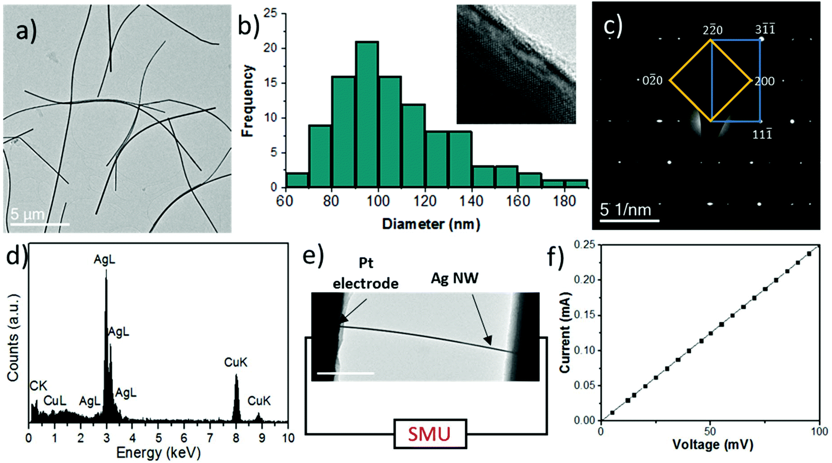 | ||
| Fig. 1 (a) Bright-field TEM image of the as-received Ag nanowires; (b) frequency distribution of the Ag nanowire diameter; the height of the bar represents the number of nanowires and the width of each bar is 10 nm, inset: a representative high-resolution TEM image showing a thin organic coating on the Ag NW surface; (c) SAED pattern of a section of an individual Ag nanowire, the yellow and blue boxes mark the set of diffraction spots from the overlapping zone axis [001] and [112], respectively; (d) EDX spectrum of the Ag nanowire (the Cu originates from the TEM sample supporting grid); (e) TEM micrograph of Ag NW-1 suspended between two Pt electrodes, along with the schematic setup for electrical measurements; (f) two-probe I–V curve of the system in (e). | ||
Using drop-casting, the Ag NWs were suspended from Pt electrodes and positioned over the through-holes of the custom-made chips (Fig. 1e). To absorb excess liquid, filter paper was placed underneath. Upon taking the chips for SEM imaging, it was observed that a good number of them hosted bent nanowires (Fig. S1c†). This can be justified by the effect of surface tension: an increasing downward force is exerted on the suspended nanowire as the IPA evaporates or gets absorbed by the filter paper. After drying, the chips were taken to the TEM where they were analysed electrically in a two-probe configuration (Fig. 1e). The voltage was first swept from 0 to 100 mV to infer the total electrical resistance of the nanowire-electrode system (the bias was kept purposely low to avoid Joule heating). Consistently, the current–voltage (I–V) curves were linear, identifying the 28 devices probed as Ohmic-type (Fig. 1f). Given that the typical contact resistance of Ag NWs with metal electrodes is <20 Ω,40,57i.e. much lower than the resistance (R) of hundreds of ohms measured for the present systems (cf. Table S1†), this term was overlooked when calculating the resistivity (ρ) of the interconnecting wires (eqn (1), where A refers to cross-sectional area and l to length):
 | (1) |
As listed in Table S1,† the resistivity varied between 1.1 × 10⁻⁷ and 5.0 × 10⁻⁸ Ω m. The average of these, 3.1 × 10⁻⁷ Ω m, is comparable to the values reported in the literature (Table S2†). Still, this is one order of magnitude higher than the resistivity of bulk Ag (1.6 × 10⁻⁸ Ω m)58 which can be justified considering the size effects, structural defects and, as mentioned above, the presence of a carbonaceous shell.27,28,36,59
3.2 Breakdown of initially straight Ag nanowires
In electrical stress studies of 1D nanostructures, the rate at which the applied bias is incremented can considerably change the outcome of the experiment.13,38,60 To evaluate this, fast- (>20 mV s−1) and slow-rate (<20 mV s−1) in situ TEM electrical probing experiments were carried out on initially straight (or almost straight) Ag NWs. When using a fast-rate regime, the interconnect breakdown took place suddenly and resulted in sectioning of the nanowire. In these cases, two opposite segments were observed with “drop-like” tips (an example, NW-2, is shown in Fig. S3 and Video 1†). By contrast, the slow-rate approach induced a different behaviour, as illustrated with NW-3 in Fig. 2a. When the bias was applied (7 mV s−1), the current flowing through the nanowire gradually increased (Fig. 2b). Throughout, a gradual drop in resistance was seen. One reasoning is the slow annealing of contacts.37,61–63 In addition, electromigration and Joule heating may have induced stress which resulted in a slight displacement of the nanowire/contacts (as seen by the downward movement signalled with the red line position marker in Fig. 2a). In this system, necking occurred and, at 2.1 V (7.5 mA), the nanowire failed (see Video 2†). “Needle-like” tips were observed (Fig. 2c and d) and the breakdown point was closer to one of the electrodes (Fig. S4†). Note that for both regimes (slow- and fast-rate), breakdown did not necessarily take place at the mid-length of the nanowires, an observation that concurs with the literature and often explained by pinning of hot-spots due to structural defects or localized lattice strain.64,65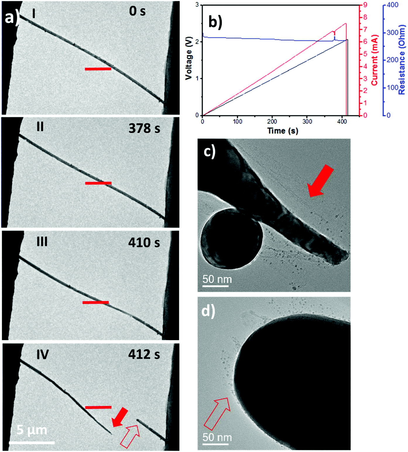 | ||
| Fig. 2 (a) Time series (panels I–IV) TEM micrographs of the NW-3 breakdown, in this (and following figures of the article), the thick red line acts as a position marker; (b) voltage vs. time curve with output datasets of current and resistance; (c, d) high magnification TEM micrographs after breakdown of NW-3, the solid and empty red arrows refer to panel IV in (a) and point to the sectioned ends of the nanowire. | ||
3.3 Breakdown of initially crooked (bent) Ag nanowires
Observing that slow bias rates provided better control over the dynamics of the interconnect breakdown process, this approach was adopted to study the response of bent Ag NWs to electrical stress. In the following, and besides nanowire sectioning, different types of behaviour are described ranging from string-like resonance (elastic deformation) to re-crystallization (plastic deformation).| ε = r/(r + Rc), | (2) |
| σ = E × ε, | (3) |
 | ||
| Fig. 3 (a) Time series (panels I–IV) TEM micrographs of the Ag NW-4 response; (b) voltage vs. time curve with output datasets of current and resistance; (c, d) TEM micrographs of the bent NW-4, before and after buckling, respectively. Inset of (d): a magnified view highlighting the carbon sleeve that restrains the sectioned ends of the nanowire. | ||
While the Young's modulus of bulk Ag is 84 GPa,66 for Ag NWs with diameters ranging from 80 to 120 nm, this value varies between 70 and 100 GPa.51,67,68 Given the diameter of 98 nm for NW-4, by assuming E = 80 GPa, its estimated bending strain and stress were 0.82% (±0.1%) and 654 MPa (±80 MPa), respectively. As the bending strain is roughly half of the reported yield figure for bulk Ag (1.5%)51 and one-fourth of the bending strain of Ag NWs (2.5–5.2%),45,46,52 plastic deformation was not expected for this nanowire with an initially crooked configuration.
In tandem with video-recording, electrical probing data (voltage, current) were collected and processed in real-time (resistance). With an initial resistance of 467 Ω, NW-4 was subjected to a monotonic increment of applied bias starting from 0 V and up to 1 V, at a rate of 10 mV s−1 (Fig. 3b). With the exception of a small drop during the first few seconds (likely due to contact adjustment), the overall resistance of this system remained constant for 35 s (blue curve in Fig. 3b). Then, for about 5 s, another resistance drop occurred, possibly from the completion of contact curing.28 Just before buckling (ca. t = 63 s), the resistance rose (as shown in Fig. 3a, the configuration of the nanowire was still stable). Immediately after (t = 65 s, ∼0.75 V), NW-4 thinned and buckled close to the left electrode (panel IV, Fig. 3a, and Video 3†). The mechanical failure resulted from a significant structural change, as illustrated by the before (Fig. 3c) and after (Fig. 3d) TEM micrographs. The formation of a hillock close to the anode and small voids near the cathode (Fig. S5†) indicated the occurrence of electromigration, a common phenomenon in metallic interconnects subjected to electrical stress.38,64,65 However, and in contrast to the straight nanowires, there was no abrupt separation of segments after breakdown. The analysis in Fig. 3c shows that the diameter of NW-4 necked to a minimum of 70 nm in the elbow region. Furthermore, a small gap originated (inset in Fig. 3d) but the disjointed wire was kept in place due to the organic coating acting as a restraining sleeve (at this stage, carbonized due to Joule heating). The final resistance of NW-4 was about 16 kΩ, indicating the role of the carbon shell (viz. nanowire gap) as an alternative but much less efficient path for conduction of electrons. It should be stated that throughout the plastic deformation process, NW-4 did not move at the contact regions (cf. Fig. S5a and S5b†).
 | ||
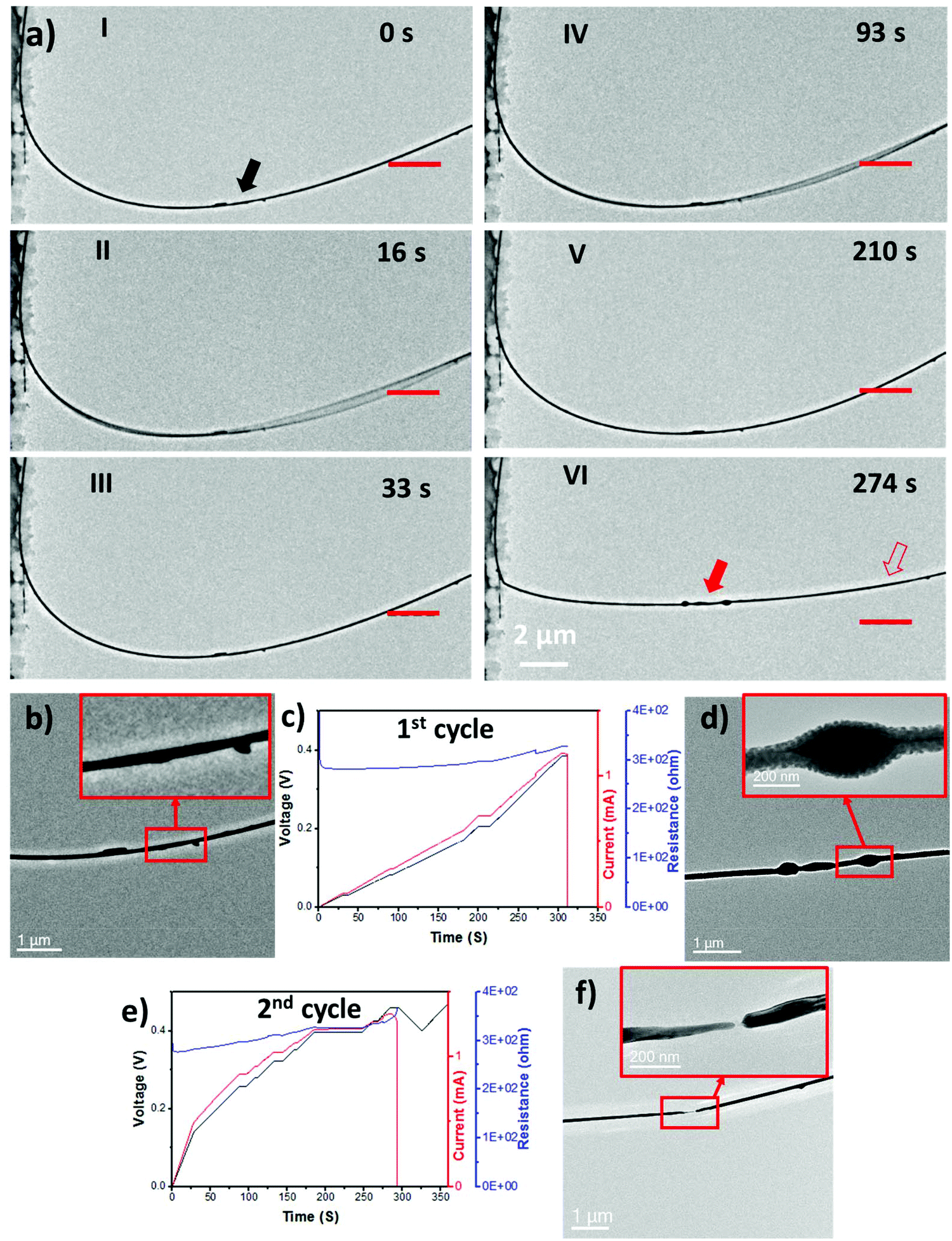
| Fig. 4 (a) Time series TEM micrographs of the Ag NW-5 response; the experiments were performed in two cycles with panels I–VI relating to the first cycle and panels I–XII to the second one; (b) high-magnification TEM micrograph of the nanowire after the first cycle; (c, d) voltage vs. time curves with output datasets of current and resistance curves for the first and second cycles, respectively; (e) high-magnification TEM micrograph of the sectioned area in NW-5, i.e. after completion of the second cycle. | ||
Following the above, NW-5 was electrically stressed until it failed. The electrical datasets and video recording for this second bias cycle are given in Fig. 4d and Video 5,† respectively. As expected, the response was equal to that of the first cycle up to t = 30 s. However, and soon after (t = 42 s, 0.85 V), an inversion of the apex direction took place confirming the existence of a second overtone (panel X, Fig. 4a). The entire sequence indicates that the suspended nanowire acts as a resonant string with the first and third harmonic modes pinned at 20 s and 42 s, respectively. Interestingly, the first overtone was not observed, possibly due to the rigidity of the contacts that impair large phase changes at the nodes of the interconnect.
Continuing with the second cycle, and after t = 42 s, the electromigration of Ag became more prominent. Failure of NW-5 occurred with a current injection of 1.3 mA (panel XI, Fig. 4a and S6†). Notwithstanding, this interconnect kept conducting charge (albeit with a much higher resistance, 15 kΩ). High-resolution imaging of the failure section shows the presence of a corrugated graphene-like film after the segmentation of the core Ag nanowire (Fig. 4e). Just as for NW-4, besides acting as a sleeve and keeping the Ag segments close-by, this carbonaceous fragment offered an alternative path for the transport of electrons (explaining the similar values of post-failure resistance for NW-4 and NW-5, see Table 1).
| NW-# | Diameter (nm) | Length (μm) | Radius of curvature (μm) | Bending strain (±0.1%) | Bending stress (±80 MPa) | Resistance before restructuring (Ω) | Resistance after restructuring (Ω) |
|---|---|---|---|---|---|---|---|
| NW-4 | 98 | 12 | 6 | 0.82% | 654 | 467 | 15![[thin space (1/6-em)]](https://www.rsc.org/images/entities/char_2009.gif) 750 750 |
| NW-5 | 85 | 20 | 12 | 0.35% | 283 | 560 | 15465 |
| NW-6 | 120 | 22 | 9 | 0.65% | 516 | 520 | 7061 |
| NW-7 | 85 | 30 | 8 | 0.53% | 425 | 320 | 360 |
Initially, the Ag NW-6 seen in Fig. 5a had an estimated bending strain and stress of 0.64 ± 0.1% and 516 ± 80 MPa, respectively. As the applied bias increased, the curved nanowire was slightly displaced from right to left (panels I–III, Fig. 5a and Video 6†). At t = 37 s (panel II, Fig. 5a), the current density passing through the radial cross-section of the 120 nm wide interconnect was 8.8 × 10⁶ A cm−2. A few seconds later (t = 40 s), the nanowire failed and its arc collapsed (panel IV, Fig. 5a). In contrast to all previous cases, the connection to the two electrodes was retained without gaps in the core Ag (i.e. no segmentation). Remarkably, the interconnect was entirely restructured in the failure zone (Fig. 5b–d). The plastic deformation, induced by electrically stressing the Ag nanowire, not only shortened the interconnect but also formed a “knot-like” section in it. Electron diffraction patterns collected from this section (Fig. S7†) demonstrate that the long-range crystalline order was lost due to the inclusion of defects commonly associated with shear bands (dislocations, twins, etc.).
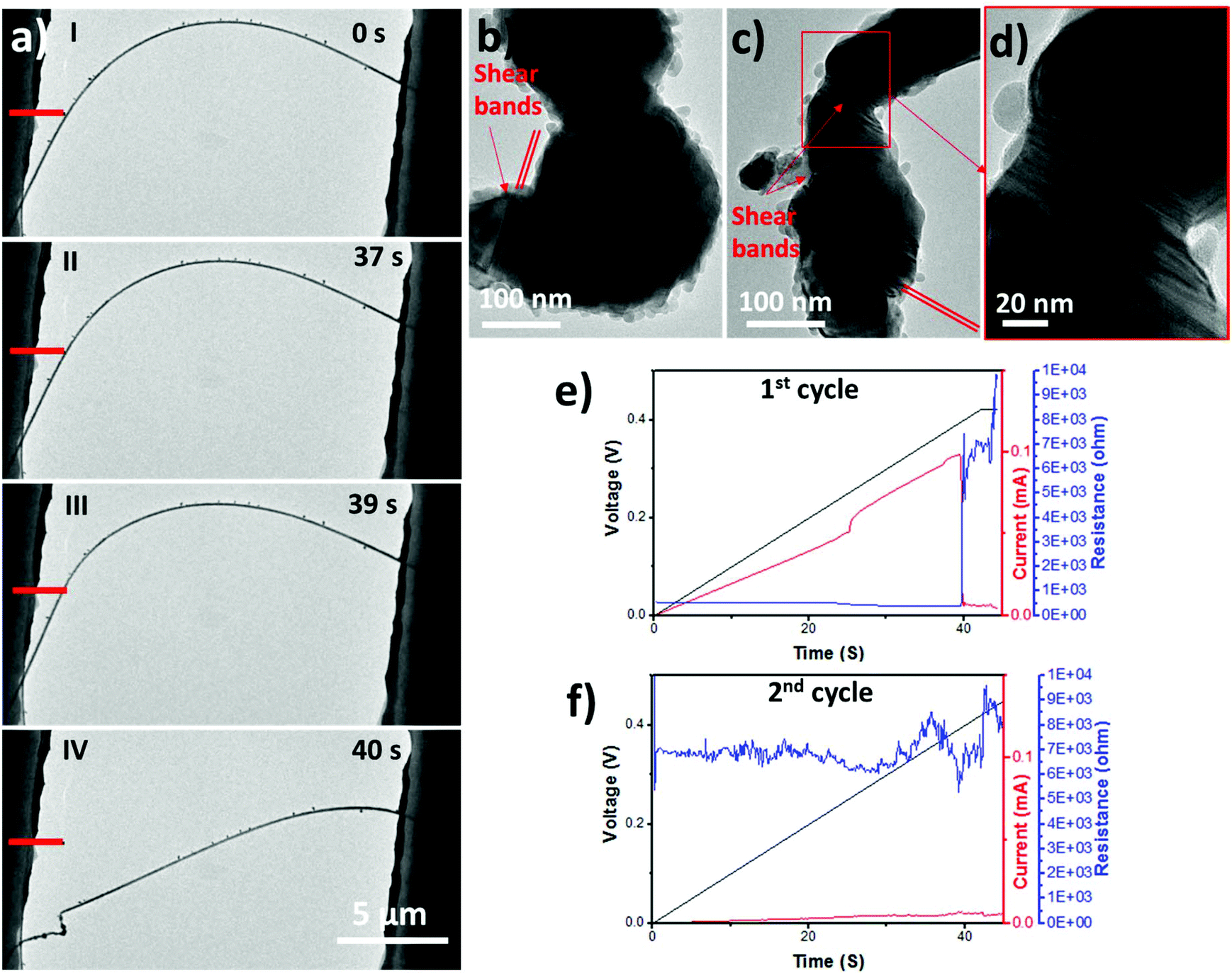 | ||
| Fig. 5 (a) Time series (panels I–IV) TEM micrographs of the Ag NW-6 response; (b–d) magnified view of the deformed “knot-like” region where shear bands and associated twins are visible (some of these are marked with thin red parallel lines); (e, f) voltage vs. time curves with output datasets of current and resistance for the first and second cycles, respectively. | ||
Throughout the first bias cycle, the current flowing through NW-6 followed the same trend as that in the previous examples (Fig. 5e). However, when the second cycle was performed (i.e. after restructuring), the resistance readings of NW-6 were much lower than the analogous ones for NW-5 (Fig. 5f). In fact, whereas the resistance increased from 560 Ω to ∼15 kΩ for NW-5, this difference was considerably smaller for NW-6 (from 516 Ω to ∼7 kΩ).
When compared to NW-4 and NW-5, the lower post-failure resistance achieved by NW-6 indicated that a non-sectioned, restructured Ag NW interconnect could retain a higher degree of charge transport capability. Further investigation confirmed and expanded on this observation. With a length of 30 μm and a diameter of 85 nm (panel I, Fig. 6a), NW-7 had an estimated bending stress of 425 ± 80 MPa (for an initial bending strain of 0.53 ± 0.1%). Soon after the bias application (t = 16 s), a section of the nanowire started to vibrate in a first-order mode (panel II, Fig. 6a and Video 7†). Unlike NW-5, this was not centred at the apex of the bent nanowire but rather in its half-length closer to the anode (i.e., the electrode on the right, not shown). It is interesting to note that the resonant behaviour is pinned to a place on the nanowire where a couple of small fragments are located (the section marked with a black arrow in Fig. 6a and magnified in Fig. 6b). Their presence may have locally damped the vibrations, which would imply a high sensitivity of this resonant system to foreign bodies. Further to this, the vibration was intermittent as it would stop (e.g. t = 33 s, panel III in Fig. 6a) and re-initiate, during the same bias cycle, in the presence of a higher current density (e.g. t = 93 s, panel IV in Fig. 6a). The discontinuity may be understood if, beyond the fundamental frequency, higher order vibration modes were partly frustrated due to the short length of the resonant section.
 | ||
| Fig. 6 (a) Time series (panels I–VI) TEM micrographs of the Ag NW-7 response during the first cycle of the applied bias; the arrows mark sections mentioned in the following panels and main text; (b) TEM micrograph of the region marked with a solid black arrow in (a), panel I, inset: magnified view of the boxed area; (c) voltage vs. time curve with output datasets of current and resistance for the first cycle; (d) TEM micrograph of the region marked with a solid red arrow in (a), panel VI, inset: a magnified view of the boxed area; (e) voltage vs. time curve with output datasets of current and resistance for the second bias cycle; (f) TEM micrograph, taken after the second cycle, of the region marked with an empty red arrow in (a), panel VI, inset: magnified view of the boxed area showing segmentation of the nanowire. | ||
As concerns the transport of charge, and up until the nanowire failed and re-structured, the current increased monotonically with the applied bias (first cycle, Fig. 6c). The curves of the first cycle proceeded in two stages: first, from t = 0 s to t = 175 s, the rate used was 1 mV s−1; then, from t = 176 s to 390 s, the rate was 1.7 mV s−1. Steps in the ramps can be seen which corresponded to periods of constant bias application. This was done to follow the stability of NW-7 under constant bias or observe the interconnect in more detail (to take high-resolution TEM micrographs, for instance). Interestingly, between t = 55 s and t = 270 s, the resistance rose continuously from 281 Ω to 320 Ω. Still during this first cycle of bias application, at t = 270 s (which corresponded to a current flow of 1.30 mA, Fig. 6c), a sudden drop in resistance was observed. This was accompanied by a very visible change in the shape of the nanowire (panel VI, Fig. 6a). Similar to NW-6, there was no segmentation of the interconnect, with restructuring taking place instead (Fig. 6d). However, while NW-6 underwent extensive plastic deformation, the structural rearrangements at the failure section of NW-7 were less conspicuous (section marked with a solid red arrow in panel VI, Fig. 6a). Nonetheless, and as seen from the inset of Fig. 6d, the crystal order of the nanowire changed to that of a polycrystalline material. Overall, the restructured region of NW-7 resembled other junctions made by the welding of two different nanowires.28,29 Again, shortening of the interconnect occurred with a reduction in the length of more than 3 μm.
To test the functional integrity of the restructured NW-7 interconnect, the bias was applied a second time (Fig. 6e). Remarkably, the resistance of the system stood at 360 Ω, which is a value similar to that before the mechanical failure (320 Ω). This observation implies that the contacts remained electrically and structurally stable, with the restructured region accounting for the 40 Ω increment. With an additional bias increase, the current flowing through the device reached a maximum value of 1.25 mA. At this point, the nanowire broke down (t = 290 s). As shown in Fig. 6f, this occurred via necking and segmentation, resulting in the formation of sharp tips akin to those seen in post-breakdown straight nanowires (cf. NW-3, Fig. 2). Most interestingly, the location of failure was not where the mended part was (marked with a solid red arrow in panel VI, Fig. 6a, see also Fig. 6d) but in another section of the nanowire (empty arrow in panel VI, Fig. 6a, see also Fig. 6e). This implies that, upon the restructuring phase, the nanowire “self-healed” and the section where the polycrystalline knot appeared was no longer the “weakest link” of the interconnect.
4. Discussion
Even though there is a body of literature that delved into the electrical breakdown mechanisms of Ag NWs, the dynamics and variables affecting this are not yet entirely clear due to the lack of real-time, high-resolution analysis of individual nanowires. It is consensual, however, that Joule heating and electromigration are the two main driving forces of this process.From the results above, it is evident that there is a range of responses from suspended Ag NWs acting as interconnects between two metal electrodes with equal work-function (Pt/Pt). These responses can be categorized according to the initial configuration of the nanowires, whether straight or bent, and the rate at which the bias is applied (Scheme 1).
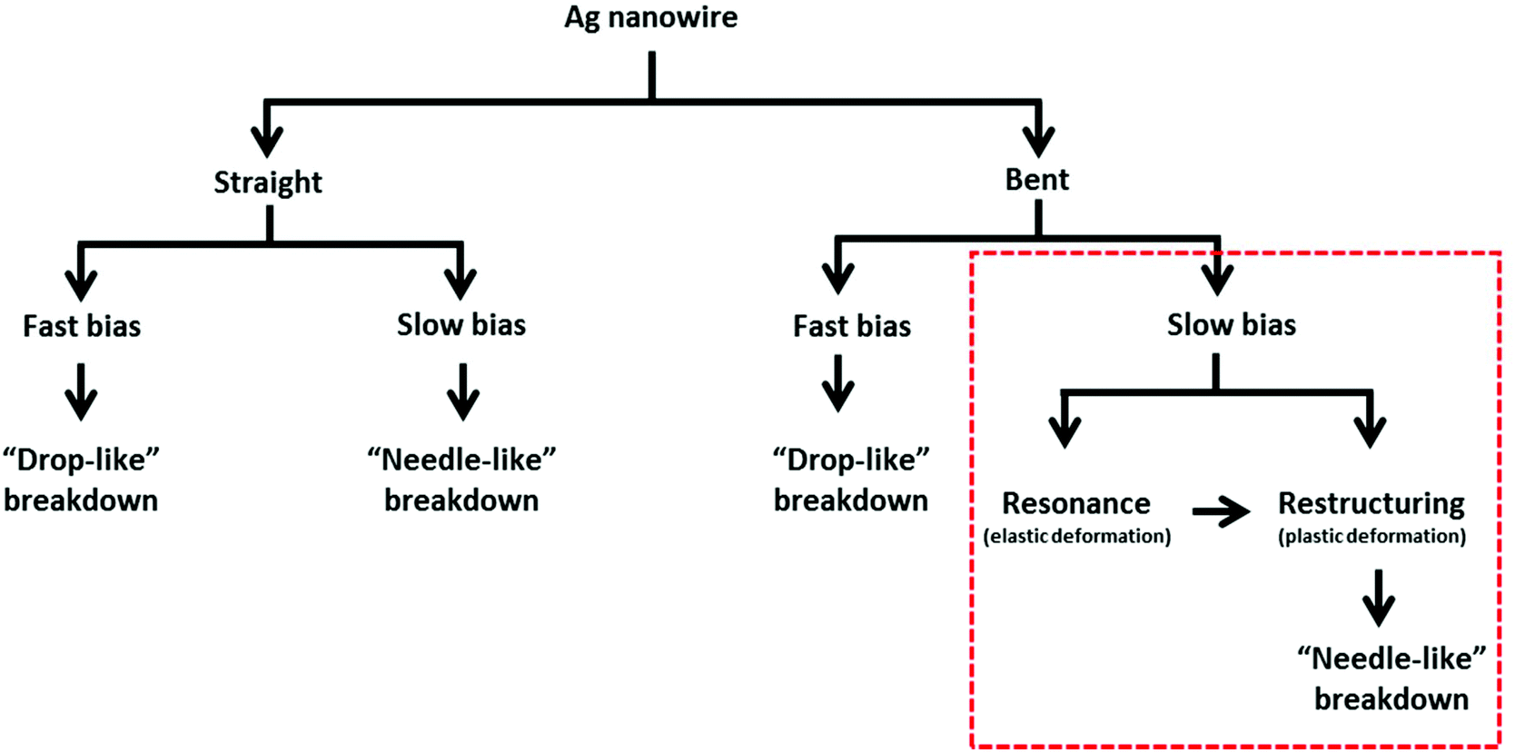 | ||
| Scheme 1 Flow chart of different current induced responses in straight and bent Ag nanowires. | ||
4.1 Straight Ag NWs
Our experiments show that if the suspended nanowire has an initially straight configuration then its breakdown will occur in one of two ways: (1) segmentation with the formation of “drop-like” ends or (2) segmentation with “needle-like” ends (Scheme 1). The case is simple as it is clearly dependent on the rate at which the threshold of current density of the interconnect is approached: fast-bias will lead to a “drop-like” segmentation whereas slow-bias will induce necking before breakdown. These observations concur with the literature. For instance, Ag NWs were utilized as resistive heaters to grow ZnO NWs in a liquid medium. For currents >8 mA, Yeo et al. reported Joule heating occurring in the Ag NW and a rapid breakdown in a “drop-like” fashion.69 On the other hand, “needle-like” breakdown of Ag NWs has been repeatedly observed and explained by the current-driven migration of atoms (and/or vacancies), these taking place preferentially around grain boundaries or via surface diffusion.38,64,65 Vafaei et al. found breakdown points of the welded nanowire at contacts, primarily due to Joule heating at nanowire–nanowire and nanowire–electrode junctions.63 However, in that work, the Ag nanowires were not suspended, rather in contact with a Si substrate. The influence that the rate at which the bias is applied was also mentioned by Hadeed et al.5 In addition, these authors stated that the location of breakdown along the length of the interconnect can differ and will depend on the type of substrate, contacts, work-function and conductivity of the electrodes as well as the medium surrounding the nanowire. In the present work, while there is no substrate-effect (suspended nanowires) and the medium is vacuum, the bending stress is also an important variable to consider.4.2 Bent Ag NWs
As expected, the suspended Ag nanowires bearing an initially crooked configuration had a more complex set of responses (Scheme 1). Besides breakdown, the bent interconnects showed two interesting phenomena: resonance and restructuring.With regard to the first, it was possible to induce a string-like resonant behaviour in a number of nanowires. This phenomenon was non-intentional and, when occurred, preceded the restructuring and breakdown phases. As far as we could observe, it did not result in plastic deformation nor did it change the contact regions of the interconnect. It is known that resonance in nanostructures can be induced by electrostatic forces,70,71 electromagnetic forces,72 opto-thermal effects73 or electron beam exposure.74,75 During our experiments, the energy of the electron beam (300 keV) and the magnetic field created by the electromagnetic lenses in the TEM remained unaltered. On the other hand, the current passing through the Ag NW was continuously increased. Note that the resonance before elastic deformation was reversible, as observed for NW-5, so we can rule out the possibility of charging induced resonances. In these circumstances, as the initial stages of resistive (or Joule) heating and electromigration developed, it is logical to assume that strain in the Ag lattice was gradually altered and that this changed the overall stiffness of the nanowire.76–78 Consequently, due to the varying internal stresses, different shapes may emerge as a mechanism to accommodate, elastically, the tension in the interconnect subjected to resistive heating. In this sense, the suspended nanowire can be considered as a string under tension. In addition to the role of current, the force exerted by the 300 keV electron beam, with a particle velocity and momentum of 3.25 × 10⁸ m s−1 and 2.95 × 10⁻²² N s, respectively, will certainly contribute to trigger a particular mode of vibration. In conclusion, the observed resonances such as those observed for NW-5 and NW-7 (with cross-sectional areas of 1.7 μm2 and 2.55 μm2, respectively) occur when the bent interconnect is electrically stressed to a point that its physical interaction with the constant electron flux (e.g. via momentum transfer) promotes the release of lattice strain build-up through a reversible shape change (elastic deformation).
Restructuring was another interesting phenomenon that preceded breakdown in bent Ag NWs. In the Results section, four representative examples of different restructuring modes are described. The main characteristics of these nanowires (NW-4 to NW-7) are listed in Table 1 (in total, 10 bent nanowires were studied in a sample population of 28 interconnects, see Table S1†).
From Tables 1 and S1,† the initial resistance for the 28 nanowires analysed fell majorly in the interval of 250–750 Ω. Recently, Bernal et al. derived a relationship between resistance and strain for suspended nanowires:39
| R(ε) = R0 + [R0(1 + 2ν)]ε, | (4) |
As mentioned above, Joule heating and electromigration can, in the first stage, alter the mechanical strength of metallic interconnects. Beyond this, and as the current density passes a threshold value that is NW-specific, softening of the interconnect is expected, followed by melting. In the present work, the Ag NWs started to melt when subjected to a current density on the order of 106 A cm−2. At this stage, and considering the slow-rates of applied bias, the bent interconnects invariably underwent a structural rearrangement (plastic deformation). Though the final configuration obtained was not uniform, restructuring can be reasoned as a (non-reversible) mechanism to relax the strained nanowires as it allows them to approximate the “straight nanowire” configuration. In this sense, and while constituting a failure event, this phenomenon did not necessarily compromise the function of the nanowires in transporting charge. For this reason, a distinction needs to be made between restructuring and breakdown for bent interconnects. As proposed in Scheme 1, breakdown refers to full segmentation of the nanowire resulting in two distant and well-separated segments (i.e. without contact between them).
During the restructuring phase (which precedes breakdown), the presence of the carbonaceous coating is critical. When carbonised, due to resistive heating under vacuum, it has a dual role since it offers an alternative path for charge conduction (albeit with a much lower conductivity than the metallic Ag) and acts as a stabilising sleeve that delays full segmentation. Logically, upon further increments of applied bias, these linking carbon layers will reach their current density threshold and disintegrate (leading to breakdown of the NW, as defined). In these cases where the rearrangement did not result in the formation of gaps along the Ag nanowire, the restructured region showed knots with varied degrees of crystalline order. In cases such as that of NW-6 (Fig. 5), the knot included several shear bands and twins, both characteristic features of metals deformed plastically by compressive forces.79,80 More remarkably, in situations such as those of NW-7 (Fig. 6), smaller crystalline grains condensed along the knot which enabled the preservation of electrical conductivity in the interconnect. It is not clear what factors localize the rearrangement but it is possible that fatigue and location of structural defects in the initial nanowire (whether closer or not from the electrodes, for instance) could play an important role. As for the re-crystallisation stage, the directionality of the relaxation, strength of the carbonaceous sleeve and/or the rate of heat dissipation could account for how fast the molten Ag re-solidifies and what the final shape/length of the knots is. Finally, past the restructuring phase, the initially crooked nanowires will break in a similar way to the straight ones. Here, the point of segmentation will be either the carbon bridge (as there will be no contact through the Ag segments) or, in the case of NWs such as NW-6 and NW-7, some other locations outside the knot region.
5. Conclusions
Suspended Ag nanowires (acting as interconnects) were stressed electrically, inside a TEM, to the point of structural breakdown. Depending on their initial configuration and the rate at which the bias was applied, the nanowires showed different mechanisms of electrical and mechanical failure. For straight interconnects, the behaviour was akin to classical metallic wires subjected to high current densities with phenomena such as electromigration and necking observed in real-time. In these cases where the suspended nanowires were initially crooked (with bending strain and stress between ±0.30–0.80% and 283–654 MPa, respectively), different failure responses were observed. Under the combined effect of high current density and bending stress, the crooked nanowires underwent structural rearrangements that, in the first stage, avoided full segmentation (or breakdown). The integrity of the connection was (partly) safeguarded by a carbonised shell enveloping the Ag nanowires. Remarkably, the restructuring event (plastic deformation) did not forcibly undermine the electrical function of the interconnect. In some instances, the conductivity of the “mended” nanowire was close to its original values. In addition to this, resonance was also identified in bent Ag nanowires. When present, it invariably preceded the structural failure (restructuring) and breakdown phases.While the above observations may be applicable only in a vacuum environment, the identification of resonance and restructuring in bent Ag nanowires could have important implications in the design and fabrication of flexi-transparent conductive films and nanoelectronic devices based on these 1D nanostructures.
Conflicts of interest
There are no conflicts of interest to declare.Acknowledgements
NMB thanks KAUST for a graduate scholarship. All authors are grateful for the financial support from the KAUST (BAS/1/1346-01-01) and acknowledge the technical assistance and collaboration from the Core Labs at KAUST. We thank Syed N. R. Kazmi and Jasmin Smajic for useful discussions and feedback.References
- T. W. Ebbesen, H. J. Lezec, H. Hiura, J. W. Bennett, H. F. Ghaemi and T. Thio, Nature, 1996, 382, 54–56 CrossRef CAS
.
- H. J. Dai, E. W. Wong and C. M. Lieber, Science, 1996, 272, 523–526 CrossRef CAS
- J. Muster, G. T. Kim, V. Krstić, J. G. Park, Y. W. Park, S. Roth and M. Burghard, Adv. Mater., 2000, 12, 420–424 CrossRef CAS
- K. S. Novoselov, A. K. Geim, S. V. Morozov, D. Jiang, Y. Zhang, S. V. Dubonos, I. V. Grigorieva and A. A. Firsov, Science, 2004, 306, 666–669 CrossRef CAS PubMed
- F. O. Hadeed and C. Durkan, Appl. Phys. Lett., 2007, 91, 123120 CrossRef
- N. M. Batra, S. P. Patole, A. Abdelkader, D. H. Anjum, F. L. Deepak and P. M. Costa, Nanotechnology, 2015, 26, 445301 CrossRef PubMed
-
E. J. Kirkland, Advanced computing in electron microscopy, Springer Science & Business Media, 2010 Search PubMed
- G. McMullan, S. Chen, R. Henderson and A. R. Faruqi, Ultramicroscopy, 2009, 109, 1126–1143 CrossRef CAS PubMed
- N. Shibata, Y. Kohno, S. D. Findlay, H. Sawada, Y. Kondo and Y. Ikuhara, J. Electron Microsc., 2010, 59, 473–479 CrossRef CAS PubMed
-
F. L. Deepak, A. Mayoral and R. Arenal, Advanced Transmission Electron Microscopy: Applications to Nanomaterials, Springer, 2015 Search PubMed
-
S. Canepa, S. B. Alam, D.-T. Ngo, K. Mølhave and F. M. Ross, in Controlled Atmosphere Transmission Electron Microscopy: Principles and Practice, ed. T. W. Hansen and J. B. Wagner, Springer, 2016, pp. 281–300. DOI:10.1007/978-3-319-22988-1_10
- D. Golberg, P. M. Costa, M. Mitome, S. Hampel, D. Haase, C. Mueller, A. Leonhardt and Y. Bando, Adv. Mater., 2007, 19, 1937–1942 CrossRef CAS
- P. M. F. J. Costa, D. Golberg, M. Mitome, S. Hampel, A. Leonhardt, B. Buchner and Y. Bando, Nano Lett., 2008, 8, 3120–3125 CrossRef CAS PubMed
- P. M. Costa, U. K. Gautam, Y. Bando and D. Golberg, Nat. Commun., 2011, 2, 421 CrossRef PubMed
- P. M. F. J. Costa, P. B. Cachim, U. K. Gautam, Y. Bando and D. Golberg, Nanotechnology, 2009, 20, 405706 CrossRef PubMed
- P. M. F. J. Costa, U. K. Gautam, M. Wang, Y. Bando and D. Golberg, Carbon, 2009, 47, 541–544 CrossRef CAS
- M. Hauder, J. Gstöttner, W. Hansch and D. Schmitt-Landsiedel, Appl. Phys. Lett., 2001, 78, 838–840 CrossRef CAS
- J. Lee, P. Lee, H. Lee, D. Lee, S. S. Lee and S. H. Ko, Nanoscale, 2012, 4, 6408–6414 RSC
- B. Bari, J. Lee, T. Jang, P. Won, S. H. Ko, K. Alamgir, M. Arshadd and L. J. Guo, J. Mater. Chem. A, 2016, 4, 11365–11371 RSC
- H. Jeong, S. Park, J. Lee, P. Won, S.-H. Ko and D. Lee, Adv. Electron. Mater., 2018, 4, 1800243 CrossRef
- J. Lee, K. An, P. Won, Y. Ka, H. Hwang, H. Moon, Y. Kwon, S. Hong, C. Kim, C. Lee and S. H. Ko, Nanoscale, 2017, 9, 1978–1985 RSC
- T. H. Seo, S. Lee, K. H. Min, S. Chandramohan, A. H. Park, G. H. Lee, M. Park, E. K. Suh and M. J. Kim, Sci. Rep., 2016, 6, 29464 CrossRef CAS PubMed
- J. Y. Kim, J. H. Jeon and M. K. Kwon, ACS Appl. Mater. Interfaces, 2015, 7, 7945–7950 CrossRef CAS PubMed
- I. Chang, T. Park, J. Lee, M. H. Lee, S. H. Ko and S. W. Cha, J. Mater. Chem. A, 2013, 1, 8541–8546 RSC
- I. Chang, T. Park, J. Lee, H. B. Lee, S. Ji, M. H. Lee, S. H. Ko and S. W. Cha, Int. J. Hydrogen Energy, 2014, 39, 7422–7427 CrossRef CAS
- I. Chang, T. Park, J. Lee, H. B. Lee, S. H. Ko and S. W. Cha, Int. J. Hydrogen Energy, 2016, 41, 6013–6019 CrossRef CAS
- J.-Y. Lee, S. T. Connor, Y. Cui and P. Peumans, Nano Lett., 2008, 8, 689–672 CrossRef CAS PubMed
- T.-B. Song, Y. Chen, C.-H. Chung, Y. M. Yang, B. Bob, H.-S. Duan, G. Li, K.-N. Tu, Y. Huang and Y. Yang, ACS Nano, 2014, 8, 2804–2811 CrossRef CAS PubMed
- E. C. Garnett, W. Cai, J. J. Cha, F. Mahmood, S. T. Connor, M. Greyson Christoforo, Y. Cui, M. D. McGehee and M. L. Brongersma, Nat. Mater., 2012, 11, 241–249 CrossRef CAS PubMed
- H. Kim, H. Lee, I. Ha, J. Jung, P. Won, H. Cho, J. Yeo, S. Hong, S. Han, J. Kwon, K.-J. Cho and S. H. Ko, Adv. Funct. Mater., 2018, 28, 1801847 CrossRef
- J. Jung, H. Lee, I. Ha, H. Cho, K. K. Kim, J. Kwon, P. Won, S. Hong and S. H. Ko, ACS Appl. Mater. Interfaces, 2017, 9, 44609–44616 CrossRef CAS PubMed
- H. Lee, S. Hong, J. Lee, Y. D. Suh, J. Kwon, H. Moon, H. Kim, J. Yeo and S. H. Ko, ACS Appl. Mater. Interfaces, 2016, 8, 15449–15458 CrossRef CAS PubMed
- H. Moon, H. Lee, J. Kwon, Y. D. Suh, D. K. Kim, I. Ha, J. Yeo, S. Hong and S. H. Ko, Sci. Rep., 2017, 7, 41981 CrossRef CAS PubMed
- L. Hu, J. W. Choi, Y. Yang, S. Jeong, F. La Mantia, L.-F. Cui and Y. Cui, Proc. Natl. Acad. Sci. U. S. A., 2009, 106, 21490–21494 CrossRef CAS PubMed
- C. K. Jeong, J. Lee, S. Han, J. Ryu, G. T. Hwang, D. Y. Park, J. H. Park, S. S. Lee, M. Byun, S. H. Ko and K. J. Lee, Adv. Mater., 2015, 27, 2866–2875 CrossRef CAS PubMed
- W. Xu and S. H. Yu, Small, 2009, 5, 460–465 CrossRef CAS PubMed
- B. J. Wiley, Z. Wang, J. Wei, Y. Yin, D. H. Cobden and Y. Xia, Nano Lett., 2006, 6, 2273–2278 CrossRef CAS PubMed
- X. Liu, J. Zhu, C. Jin, L. M. Peng, D. Tang and H. Cheng, Nanotechnology, 2008, 19, 085711 CrossRef PubMed
- R. A. Bernal, T. Filleter, J. G. Connell, K. Sohn, J. Huang, L. J. Lauhon and H. D. Espinosa, Small, 2014, 10, 725–733 CrossRef CAS PubMed
- J. Wang, Z. Wu, C. Mao, Y. Zhao, J. Yang and Y. Chen, Sci. Rep., 2018, 8, 4862–4869 CrossRef PubMed
- P. Gao, Z. Z. Wang, K. H. Liu, Z. Xu, W. L. Wang, X. D. Bai and E. G. Wang, J. Mater. Chem., 2009, 19, 1002–1005 RSC
- W. Wang, Q. Yang, F. Fan, H. Xu and Z. L. Wang, Nano Lett., 2011, 11, 1603–1608 CrossRef CAS PubMed
- E. K. McCarthy, A. T. Bellew, J. E. Sader and J. J. Boland, Nat. Commun., 2014, 5, 4336 CrossRef CAS PubMed
- X. Xia, B. Yang, X. Zhang and C. Zhou, Mater. Res. Express, 2015, 2, 075009 CrossRef
- B. Hwang, T. Kim and S. M. Han, Extreme Mech. Lett., 2016, 8, 266–272 CrossRef
- B. Hwang, J. G. Seol, C.-H. An and S. H. Kim, Thin Solid Films, 2017, 625, 1–5 CrossRef CAS
-
N. M. Batra and P. M. F. J. Costa, US Pat., 62/677333, 2018 Search PubMed
- X. Sun and Y. Li, Langmuir, 2005, 21, 6019–6024 CrossRef CAS PubMed
- X. Tan, Z. Wang, J. Yang, C. Song, R. Zhang and Y. Cui, Nanotechnology, 2009, 20, 445102 CrossRef PubMed
- H. Chen, Y. Gao, H. Zhang, L. Liu, H. Yu, H. Tian, S. Xie and J. Li, J. Phys. Chem. B, 2004, 108, 12038–12043 CrossRef CAS
- Y. Zhu, Q. Qin, F. Xu, F. Fan, Y. Ding, T. Zhang, B. J. Wiley and Z. L. Wang, Phys. Rev. B: Condens. Matter, 2012, 85, 045443 CrossRef
- D. Kim, S. H. Kim, J. H. Kim, J. C. Lee, J. P. Ahn and S. W. Kim, Sci. Rep., 2017, 7, 45903 CrossRef CAS PubMed
- Y. Gao, P. Jiang, D. F. Liu, H. J. Yuan, X. Q. Yan, Z. P. Zhou, J. X. Wang, L. Song, L. F. Liu, W. Y. Zhou, G. Wang, C. Y. Wang and S. S. Xie, Chem. Phys. Lett., 2003, 380, 146–149 CrossRef CAS
- X. Sun and Y. Li, Adv. Mater., 2005, 17, 2626–2630 CrossRef CAS
- J. Schwan, S. Ulrich, V. Batori, H. Ehrhardt and S. R. P. Silva, J. Appl. Phys., 1996, 80, 440–447 CrossRef CAS
- Y. Wang, X. Zhao, Y. Tian, Y. Wang, A. K. Jan and Y. Chen, Chemistry, 2017, 23, 419–426 CrossRef CAS PubMed
-
J. Wang, Z. Wu, C. Mao, J. Yang, Y. Ding, Y. Chen and Z. Ni, Proceedings of the Asian Conference on Thermal Sciences, 2017, pp. 1–4
- R. A. Matula, J. Phys. Chem. Ref. Data, 1979, 5, 1147–1179 CrossRef
- Z. Cheng, L. Liu, M. Lu and X. Wang, Sci. Rep., 2015, 5, 10718 CrossRef CAS PubMed
- P. M. F. J. Costa, U. K. Gautam, Y. Bando and D. Golberg, Carbon, 2011, 49, 3747–3754 CrossRef CAS
- H. Tohmyoh, J. Appl. Phys., 2009, 105, 014907 CrossRef
- D. P. Langley, M. Lagrange, G. Giusti, C. Jimenez, Y. Brechet, N. D. Nguyen and D. Bellet, Nanoscale, 2014, 6, 13535–13543 RSC
- A. Vafaei, A. Hu and I. A. Goldthorpe, Nano-Micro Lett., 2014, 6, 293–300 CrossRef
- J. Zhao, H. Sun, S. Dai, Y. Wang and J. Zhu, Nano Lett., 2011, 11, 4647–4651 CrossRef CAS PubMed
- P. S. Ho and T. Kwok, Rep. Prog. Phys., 1989, 52, 301–348 CrossRef CAS
-
T. H. Courtney, Mechanical Behavior of Materials, Waveland Press, USA, 2005 Search PubMed
- S. Vlassov, B. Polyakov, L. M. Dorogin, M. Antsov, M. Mets, M. Umalas, R. Saar, R. Lõhmus and I. Kink, Mater. Chem. Phys., 2014, 143, 1026–1031 CrossRef CAS
- D. Alducin, R. Borja, E. Ortega, J. J. Velazquez-Salazar, M. Covarrubias, F. M. Santoyo, L. Bazán-Díaz, J. E. Sanchez, N. Torres, A. Ponce and M. José-Yacamán, Scr. Mater., 2016, 113, 63–67 CrossRef CAS
- J. Yeo, G. Kim, S. Hong, J. Lee, J. Kwon, H. Lee, H. Park, W. Manoroktul, M. T. Lee, B. J. Lee, C. P. Grigoropoulos and S. H. Ko, Small, 2014, 10, 5015–5022 CrossRef CAS PubMed
- S. N. Kazmi, M. A. Hafiz, K. N. Chappanda, S. Ilyas, J. Holguin, P. M. Costa and M. I. Younis, Nanoscale, 2017, 9, 3449–3457 RSC
- D. A. Dikin, X. Chen, W. Ding, G. Wagner and R. S. Ruoffa, J. Appl. Phys., 2003, 93, 226–230 CrossRef CAS
- X. L. Feng, R. He, P. Yang and M. L. Roukes, Nano Lett., 2007, 7, 1953–1959 CrossRef CAS
- R. De Alba, T. S. Abhilash, R. H. Rand, H. G. Craighead and J. M. Parpia, Nano Lett., 2017, 17, 3995–4002 CrossRef CAS PubMed
- J. Su and X. Zhu, RSC Adv., 2017, 7, 45691–45696 RSC
- P. Vincent, S. Perisanu, A. Ayari, M. Choueib, V. Gouttenoire, M. Bechelany, A. Brioude, D. Cornu and S. T. Purcell, Phys. Rev. B: Condens. Matter, 2007, 76, 085435 CrossRef
-
L. Xu, J. H. L. Pang, F. Ren, X. Zhang, J.-W. Nah and K. N. Tu, Electronics Packaging Technology Conference, 2006, pp. 760–765
- X. J. Wang, Q. L. Zeng, Q. S. Zhu, Z. G. Wang and J. K. Shang, J. Mater. Sci. Technol., 2010, 26, 737–742 CrossRef CAS
- J. R. P. Carreker, J. Met., 1957, 112–115 Search PubMed
- S. Lee, J. Im, Y. Yoo, E. Bitzek, D. Kiener, G. Richter, B. Kim and S. H. Oh, Nat. Commun., 2014, 5, 3033 CrossRef PubMed
- J. Wang, Y. Wang, W. Cai, J. Li, Z. Zhang and S. X. Mao, Sci. Rep., 2018, 8, 4574–4581 CrossRef PubMed
Footnote |
| † Electronic supplementary information (ESI) available: Sample loading for TEM chips, characterisation of the as-received Ag NWs, a list of NWs studied, literature survey, analysis of failed and restructured nanowires, SAED patterns of restructured regions, and video-recording of electrical stress responses of Ag NWs. See DOI: 10.1039/c8nr08551j |
| This journal is © The Royal Society of Chemistry 2019 |