
 Open Access Article
 This Open Access Article is licensed under a Creative Commons Attribution-Non Commercial 3.0 Unported Licence
A sub 20 nm metal-conjugated molecule junction acting as a nitrogen dioxide sensor†
Ishtiaq H.
Wani
 ad,
S. Hassan M.
Jafri
*ad,
John
Warna
b,
Aqib
Hayat
a,
Hu
Li
a,
Vivek A.
Shukla
b,
Andreas
Orthaber
c,
Anton
Grigoriev
b,
Rajeev
Ahuja
b and
Klaus
Leifer
*a
ad,
S. Hassan M.
Jafri
*ad,
John
Warna
b,
Aqib
Hayat
a,
Hu
Li
a,
Vivek A.
Shukla
b,
Andreas
Orthaber
c,
Anton
Grigoriev
b,
Rajeev
Ahuja
b and
Klaus
Leifer
*a
aApplied Materials Science, Department of Engineering Sciences, Uppsala University, Box 534, Uppsala SE-75121, Sweden. E-mail: Klaus.leifer@angstrom.uu.se
bCondensed Matter Theory, Department of Physics and Astronomy, Uppsala University, Box 516, Uppsala SE-75120, Sweden
cMolecular Inorganic Chemistry, Department of Chemistry/Ångström, Uppsala University, Uppsala SE-75120, Sweden
dDepartment of Electrical Engineering, Mirpur University of Science and Technology (MUST) Mirpur Azad Kashmir, 10250, Pakistan. E-mail: Hassan.Jafri@must.edu.pk
First published on 18th March 2019
Abstract
The interaction of a gas molecule with a sensing material causes the highest change in the electronic structure of the latter, when this material consists of only a few atoms. If the sensing material consists of a short, conductive molecule, the sensing action can be furthermore probed by connecting such molecules to nanoelectrodes. Here, we report that NO2 molecules that adhere to 4,4′-biphenyldithiol (BPDT) bound to Au surfaces lead to a change of the electrical transmission of the BPDT. The related device shows reproducible, stable measurements and is so far the smallest (<20 nm) gas sensor. It demonstrates modulation of charge transport through molecules upon exposure to nitrogen dioxide down to concentrations of 55 ppb. We have evaluated several devices and exposure conditions and obtained a close to linear dependence of the sensor response on the gas concentration.
Single molecule electrical circuits containing components such as diodes, transistors and sensors were predicted1 and to date, many of these constituents have been demonstrated.2–4 With the help of specialized techniques and laboratory setups such as STM-break junctions,5,6 mechanically controllable break junctions (MCBJs)7 and conductive AFM,8 many exotic short chain molecules with various functionalities have been characterized. But these setups operate under very special conditions with respect to the temperature, environment and long term stability of the trapped molecule. It thus appears to be difficult to use them for sensor measurements where the sensor often requires to be positioned in a variety of environments, places and chambers. A portable nano molecular electronic device (nanoMoED) that is reproducible and retrieves its electrical response from the electronic structure of molecules that bridge gold surfaces was proposed and demonstrated.9
When setting up an experiment to obtain the ultimate sensitivity of the surface of a material to the interaction with single gas molecules, one of the ingredients of the device is a sensor surface consisting of as few atoms as possible. In this case, the modification of the electronic structure of the sensor material after interaction with the gas would be strong, meaning that one could expect the change in the electronic structure to be an important fraction of characteristic magnitudes such as energy gaps and density of states. In the case of a chemiresistor, this can only be achieved by highly conducting materials containing few atoms so that, in principle, conductive small conjugated molecules are excellent candidates for this approach.
In previous studies on gas sensors based on nanomaterials such as graphene,10,11 carbon nanomaterials12 and other 2D materials like phosphorene,13 the change of the electronic structure of the sensing material upon adhesion of a gas has been demonstrated in chemiresistor measurements. The electronic structure of the carbon containing hexagonal rings in graphene and CNTs is different from the electronic structure of small conjugated molecules containing phenyl rings. However, the adhesion of gas molecules like NO2, one of the most harmful gases in cities,14 to the phenyl rings and their effect on its electronic structure makes it possible to fabricate a nanometric sized sensor with short organic molecules such as BPDT. This could lead to a molecular electronics based sensor which would have the advantage that the sensing molecules can be synthesized in a variety of shapes and constituents and thus the gas–molecule interaction could be tuned by the choice of the molecule and finally the gas sensor response and selectivity could be influenced, if not determined by the choice of the molecule.
The possibility of sensing gases and ions by using molecular electronics has been theoretically predicted. Metalloporphyrins change their conductivity upon interaction with gas molecules i.e. O2, CO, NO2, and NO.15 Kondo et al. predicted that an iron porphyrin based gas sensor has a distinct bias voltage behavior for different gases such as O2, CO, and NO.16 Qusiy Al-Galiby et al. suggested that the conductance of perylene diimide changes in the presence of electron acceptors (TNT, tetracyanoethylene) and donors (bis(ethylenedithio)tetrathiafulvalene).17
Experimentally, conductance switching in tetrathiafulvalene could be initiated in liquids by cyclic redox reactions.18 Gas sensing by molecules has been demonstrated using thin films of polymers. A conductance change in the thin film of oligophenylene-vinylene (OPV) in the presence of different aromatic molecules was observed.19 Electrical circuits based on organic thin films and polymers are electronic devices retrieving some of their properties from the electronic structure of the molecules and they have been used for sensing applications. Polyaniline (PANI) based gas and vapor sensors20 and poly(3-hexylthiophene) (P3HT) based volatile organic compound sensors21 are examples using this class of molecules. The sensing action in such thin film devices can have multiple origins such as changes of the conductivity of the polymer thin film by gases adsorbing onto grain boundaries, change of the spacing between polymer chains in the presence of gases or charge transfer between the gas and the molecule.
Here, we demonstrate a 20 nm molecular electronic device that shows a significant change in the conductivity of biphenyl dithiol (BPDT) molecules upon interaction with NO2 gas in an experimental setup that derives its electrical properties from the electronic structure of the single molecule. Density functional theory (DFT) simulations support these findings. We have developed a molecular electronic platform consisting of 20 nm spaced gold nanoelectrodes bridged by functionalized gold nanoparticles.22,23 In these nanoMoEDs, the electrons are transported between the nanoelectrodes through a conductive chain where the individual member of the chain consists of thiol terminated molecules bound to a gold nanoparticle (AuNP) surface.22,24,25 We could show that for a gap size of ≈20 nm and 5 nm AuNPs used in this work, the electrical current will flow through a chain consisting of 4–6 AuNP–molecule junctions. Furthermore, the electrical response of the device retains the single molecule signature as shown in inelastic tunneling spectroscopy measurements.9
To prepare this platform for gas sensing measurements, the ω-thiol protected α,ω-octane dithiol functionalized gold AuNPs were trapped in the nanoelectrode gap by dielectrophoresis.26 The junction between the molecule and the Au surfaces is then formed by inserting BPDT molecules through a place exchange reaction.27 The place exchange manifests by a resistance drop of 2–3 orders of magnitude (ESI Fig. S1†). This indicates that the BPDT is bound by chemisorption to the Au surfaces, which are either Au-electrode–BPDT–AuNP or AuNP–BPDT–AuNP junctions (Fig. 1A, B and ESI Fig. S1†). The stable and portable devices on a Si/SiO2 wafer22,28 are brought into contact electrically and can be exposed to external stimuli such as light and environmental gases. The devices are stable over time and thus are appropriate to follow the chemiresistor behavior of the BPDT based junctions exposed to gas molecules for several hours or even days.
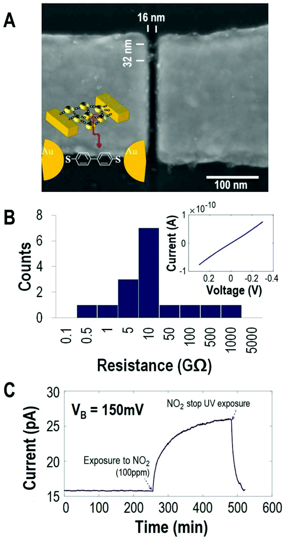 | ||
| Fig. 1 Structure, electrical properties and response upon exposure of the nanoMoED to NO2. (A) SEM image showing trapped AuNPs inside the nanogap. Inset: Schematic of the final device where AuNPs and gold surfaces are linked with BPDT molecules. (B) Resistance histogram of 16 devices, measured at 150 mV. The majority of the devices show a resistance between 1 GΩ and 10 GΩ. Inset: Typical current–voltage curve of a typical device. (C) Current versus time graph showing the electron transport through a nanoMoED at an applied bias voltage of 150 mV, in a 100 ppm NO2 environment with N2 as a carrier gas. | ||
During the gas sensing measurements, the nanoMoEDs are at a constant bias voltage VB while exposing them to a range of concentrations of NO2 at room temperature in a closed chamber (see the ESI† for the experimental setup) and recording the electron transport through the individual device. In the first stage of the measurement, while the device is exposed to N2 (Fig. 1C), the electrical current through the nanoMoED stays constant at 15.8 pA ± 20 fA. Upon exposure to 100 ppm NO2 (in N2), the current increases to 26 pA ± 50 fA. The response R is 64% above the baseline current and is calculated as

After purging the chamber with N2 gas and illuminating the sample with UV light, the current decreases rapidly to the base current.
Under the same exposure conditions, all devices showed a clear increase of the current in the presence of 100 ppm NO2. Table 1 summarizes the response R observed for 6 devices. The average percentage response is C = 54 ± 12% and ESI Fig. S2† shows the individual current time response.
| Device no | Applied voltage | Percentage response (%) |
|---|---|---|
| 1 | 150 mV | 39.5% |
| 2 | 150 mV | 67.8% |
| 3 | 100 mV | 54.7% |
| 4 | 150 mV | 63.9% |
| 5 | 150 mV | 66.28% |
| 6 | 150 mV | 66.1% |
Nonequilibrium Green's function (NEGF) combined with density functional theory (DFT) calculations (see the ESI† for the detailed method) on the BPDT connected with gold electrodes at both the ends predicts the availability of additional transport channels when NO2 is either chemisorbed or physisorbed as shown in Fig. 2.
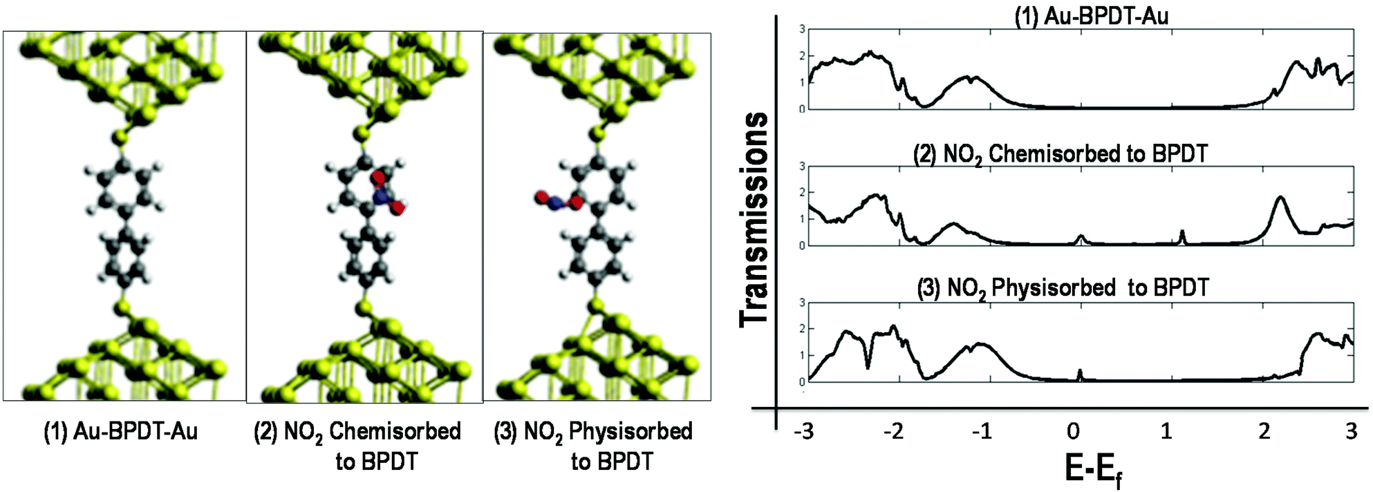 | ||
| Fig. 2 Transmission plots for three types of systems: (1) BPDT bridging gold electrodes and without a gas molecule, (2) BPDT bridging gold electrodes and with a NO2 molecule chemisorbed on it and (3) BPDT bridging gold electrodes and with a NO2 molecule physisorbed on it. | ||
In the chemisorbed case, the gas molecule binds to the BPDT molecule, which is reflected in the changes in transmission, including the changed transmission of the BPDT HOMO and LUMO-related states. Also, a broadening of the NO2 state at the Fermi level is observed which does not happen in the physisorbed case and which is due to better coupling of the electronic states to the continuum of the states induced from gold electrodes.
In the physisorbed case, the gas molecule just slightly influences the BPDT molecule and the peak at the Fermi level is due to an extra state coming from the gas molecule. The calculated adsorption energies using the LDA/GGA of the NO2 molecule on BPDT are 1.04/0.43 eV in the case of chemisorption and 2.04/0.64 eV in the case of physisorption. It is thus worthwhile to emphasize that this is one of the rare cases where the chemisorbed state is less stable than the physisorbed one. If NO2 is trapped between two benzene rings of two closely adsorbed BPDT molecules, then the binding energy is 0.94 eV. Thus, both binding configurations should yield a very stable NO2–BPDT interaction as well as lead to an increase in the conductivity of the NO2–BPDT complex as compared to only BPDT.
In a control experiment, we verified the importance of the BPDT–NO2 interaction. For this purpose, the nano-MoED containing only the ω-thiol protected α,ω-octanedithiol functionalized gold NPs was exposed to 100 ppm of NO2 gas. No significant change in electron transport was observed (see the ESI†).
Theoretical calculations and simulations where the α,ω-octane dithiol molecules were exposed to NO2 show that NO2 was only loosely bonded with a negligible effect on the conductivity (see the ESI† for details). The reproducibility of the sensor response upon NO2 gas flux was analyzed by exposing the nano-MoED repeatedly to 1 ppm NO2 gas concentration (Fig. 3A) where the devices are reset by exposure to a low intensity of UV irradiation.
 | ||
| Fig. 3 Response of the nanoMoED is repeatable and it increases with increasing concentration. (A) Repeatedly observed response of 17.62 ± 0.42% at 1 ppm concentration of NO2 for one of the devices. Points 1, 2, and 3 are the instances of 1 ppm NO2 injection whereas 1′, 2′ and 3′ are the instances of stopping NO2 and illuminating the chemiresistor with UV light under an N2 atmosphere. (B) Concentration versus response relationship for one of the chemiresistors is used to evaluate the adsorption kinetics of NO2. (C) Linear fitting of the concentration versus response data to calculate the sensitivity and detection limit of the nanoMoED. | ||
Exposure to higher concentrations of NO2 leads to higher saturation levels of the current through the BPDT molecules as shown in Fig. 3B.
To understand the kinetics of the gas sensor and its detection limits, we measured its electrical response at various input NO2 concentrations and used the Langmuir isotherm to evaluate the sensor performance parameters.29 ESI Fig. S3† shows the variable concentration response and application of the Langmuir model. The sticking probability for our NO2-chemiresistor calculated from the experimental data is 1.83 × 10⁻³ and the value of binding energy of our system is between 0.8 eV and 0.9 eV. Fig. 3C shows the linear region of response versus the concentration curve with the changing concentration of NO2. The error bars are an estimate of the variation in response to repeated exposures to a fixed concentration of the NO2/N2 mixture. The slope of the linear fit gives the sensitivity of this sensor device which is 13% ppm−1. The detection limit of the device is determined to be 55 ppb as described in ESI Fig. S3.†
In fact, optically read out, plasmonic near field sensors were shown to be miniaturized where the sensing nanoparticles were about 60 nm in diameter and the sensing unit, antenna plus nanoparticles, was as small as about 200 nm.30 The size of the nanoMoED sensor, 20 nm, is thus remarkably small. The peak concentration limits of NO2 harmful to human health are of the order of 100 ppm.31 Thus, this single 20 nm sized sensor reaching sensitivities of 55 ppb can be used as a nano-gas sensor in concentration ranges that are very useful for applications to date.
Conclusions
We have shown that BPDT molecules change their electrical conductivity upon interaction with NO2 molecules, confirmed by both theoretical and experimental work. Using this novel short chain molecule based sensor phenomenon, the first systematic gas sensor experiments with a device size of 20 nm and BPDT as a sensing element showed a reproducible and repeatable change in electrical resistance in the presence of NO2. The resistance decreases upon increasing the concentration of NO2 in the environment. From DFT simulations, the increased electrical transmission can be related to the additional states at the Fermi level when NO2 is either chemisorbed or physisorbed onto the BPDT. The sensitivity of one of our devices is calculated to be 13% per ppm and its detection limit is 55 ppb. This sensing phenomenon can be the base for novel future sensor devices.Conflicts of interest
There are no conflicts to declare.Acknowledgements
We thank U3MEC at Uppsala University, especially Henrik Ottosson and Andreas Wallner, for helpful discussions. We are grateful for financial support from the Uppsala University priority center KoF-U3MEC, the Swedish Research Council (Vetenskapsrådet), the Knut and Alice Wallenberg Foundation, the Göran Gustafsson Foundation, the Carl Tryggers Stiftelse för Vetenskaplig Forskning, the Swedish Energy Agency, the Stiftelsen för Strategisk Forskning (SSF (SUSBATT)) and the European Erasmus fellowship program. The calculations were performed at the Swedish National Infrastructure for Computing (SNIC) centers NSC (Triolith) and HPC2N (Abisko).References
- D. Xiang, X. Wang, C. Jia, T. Lee and X. Guo, Chem. Rev., 2016, 116, 4318–4440 CrossRef CAS PubMed.
- X. Yin, Y. Zang, L. Zhu, J. Z. Low, Z.-F. Liu, J. Cui, J. B. Neaton, L. Venkataraman and L. M. Campos, Sci. Adv., 2017, 3, 2615 CrossRef PubMed.
- Z. Liu, S. Ren and X. Guo, Top. Curr. Chem., 2017, 375, 56 CrossRef.
- X. Chen, M. Roemer, L. Yuan, W. Du, D. Thompson, E. del Barco and C. A. Nijhuis, Nat. Nanotechnol., 2017, 12, 797 CrossRef CAS PubMed.
- S. V. Aradhya and L. Venkataraman, Nat. Nanotechnol., 2013, 8, 399 CrossRef CAS PubMed.
- M. A. Reed, C. Zhou, C. J. Muller, T. P. Burgin and J. M. Tour, Science, 1997, 278, 252–254 CrossRef CAS.
- C. Huang, A. V. Rudnev, W. Hong and T. Wandlowski, Chem. Soc. Rev., 2015, 44, 889–901 RSC.
- T. W. Kelley, E. L. Granstrom and C. D. Frisbie, Adv. Mater., 1999, 11, 261–264 CrossRef CAS.
- S. H. M. Jafri, H. Löfås, J. Fransson, T. Blom, A. Grigoriev, A. Wallner, R. Ahuja, H. Ottosson and K. Leifer, Nanoscale, 2013, 5, 4673–4677 RSC.
- S. S. Varghese, S. Lonkar, K. K. Singh, S. Swaminathan and A. Abdala, Sens. Actuators, B, 2015, 218, 160–183 CrossRef CAS.
- Y. Hajati, T. Blom, S. H. M. Jafri, S. Haldar, S. Bhandary, M. Z. Shoushtari, O. Eriksson, B. Sanyal and K. Leifer, Nanotechnology, 2012, 23, 505501 CrossRef CAS PubMed.
- E. Llobet, Sens. Actuators, B, 2013, 179, 32–45 CrossRef CAS.
- S. Cui, H. Pu, S. A. Wells, Z. Wen, S. Mao, J. Chang, M. C. Hersam and J. Chen, Nat. Commun., 2015, 6, 8632–8632 CrossRef CAS.
- M. Chiusolo, E. Cadum, M. Stafoggia, C. Galassi, G. Berti, A. Faustini, L. Bisanti, M. A. Vigotti, M. P. Dessì, A. Cernigliaro, S. Mallone, B. Pacelli, S. Minerba, L. Simonato, F. Forastiere and G. EpiAir Collaborative, Environ. Health Perspect., 2011, 119, 1233–1238 CrossRef CAS PubMed.
- H. Liu, Z. Xu, N. Wang, C. Yu, N. Gao, J. Zhao and N. Li, J. Chem. Phys., 2010, 132, 244702 CrossRef PubMed.
- H. Kondo, J. Nara and T. Ohno, J. Phy. Chem. C, 2011, 6886–6892 CrossRef CAS.
- Q. Al-Galiby, I. Grace, H. Sadeghi and C. J. Lambert, J. Mater. Chem. C, 2015, 3, 2101–2106 RSC.
- J. Liao, J. S. Agustsson, S. Wu, C. Schönenberger, M. Calame, Y. Leroux, M. Mayor, O. Jeannin, Y.-F. Ran, S.-X. Liu and S. Decurtins, Nano Lett., 2010, 10, 759–764 CrossRef CAS PubMed.
- J. Del Re, M. H. Moore, B. R. Ratna and A. Szuchmacher Blum, Phys. Chem. Chem. Phys., 2013, 15, 8318 RSC.
- I. Fratoddi, I. Venditti, C. Cametti and M. V. Russo, Sens. Actuators, B, 2015, 220, 534–548 CrossRef CAS.
- P. Lienerth, S. Fall, P. Lévêque, U. Soysal and T. Heiser, Sens. Actuators, B, 2016, 225, 90–95 CrossRef CAS.
- H. Li, I. H. Wani, A. Hayat, S. H. M. Jafri and K. Leifer, Appl. Phys. Lett., 2015, 107, 103108 CrossRef.
- T. Blom, K. Welch, M. Strømme, E. Coronel and K. Leifer, Nanotechnology, 2007, 18, 285301 CrossRef.
- S. H. M. Jafri, T. Blom, K. Leifer, M. Strømme, H. Löfås, A. Grigoriev, R. Ahuja and K. Welch, Nanotechnology, 2010, 21, 435204 CrossRef CAS PubMed.
- S. H. M. Jafri, H. Löfås, T. Blom, A. Wallner, A. Grigoriev, R. Ahuja, H. Ottosson and K. Leifer, Sci. Rep., 2015, 5, 14431 CrossRef CAS PubMed.
- A. Wallner, S. H. M. Jafri, T. Blom, A. Gogoll, K. Leifer, J. Baumgartner and H. Ottosson, Langmuir, 2011, 27, 9057–9067 CrossRef CAS PubMed.
- J. Liao, S. Blok, S. J. van der Molen, S. Diefenbach, A. W. Holleitner, C. Schönenberger, A. Vladyka and M. Calame, Chem. Soc. Rev., 2015, 44, 999–1014 RSC.
- S. H. M. Jafri, T. Blom, A. Wallner, H. Ottosson and K. Leifer, J. Nanopart. Res., 2014, 16, 2811 CrossRef.
- W. Wongwiriyapan, S. Inoue, S.-I. Honda and M. Katayama, Jpn. J. Appl. Phys., 2008, 47, 8145–8147 CrossRef CAS.
- N. Liu, M. L. Tang, M. Hentschel, H. Giessen and A. P. Alivisatos, Nat. Mater., 2011, 10, 631 CrossRef CAS PubMed.
- Air Quality Air Quality Guidelines, WHO Regional Office for Europe, 2006.
Footnote |
| † Electronic supplementary information (ESI) available: Materials and methods, results of exposure of the molecular nanoMoED to nitrogen dioxide and calculation/measurement of binding energy and sticking probability. See DOI: 10.1039/c8nr08417c |
| This journal is © The Royal Society of Chemistry 2019 |