
Direct observation of quantum tunnelling charge transfers between molecules and semiconductors for SERS†
Nam-Jung
Kim
 ab,
Jayeong
Kim
c,
Jun-Beom
Park
b,
Hyemin
Kim
c,
Gyu-Chul
Yi
b and
Seokhyun
Yoon
*c
ab,
Jayeong
Kim
c,
Jun-Beom
Park
b,
Hyemin
Kim
c,
Gyu-Chul
Yi
b and
Seokhyun
Yoon
*c
aDepartment of Mechanical & Aerospace Engineering, University of Missouri, Columbia, MO 65211, USA
bSchool of Physics, Seoul National University, Seoul, 08826, Korea
cDepartment of Physics, Ewha Womans University, Seoul, 03760, Korea. E-mail: syoon@ewha.ac.kr
First published on 26th November 2018
Abstract
We used high-quality ZnO nanostructures/graphene substrates for understanding the mechanisms of charge transfer (CT) that take place under nonplasmonic conditions. As the optimal conditions for CT processes are found, we studied the range of CT normal to the ZnO surface that is coated with nanoscale HfO2 layers with different thicknesses. We could observe that CT decays over a few nanometers. In addition, we also observed a unique oscillation of the SERS intensity in the atomically thin oxide layers, which reflects the quantum tunneling effects of CT electrons across the oxide layers. To the best of our knowledge, this is the first direct observation of SERS-active charge transport and measurement of a CT span with atomic-scale accuracy.
Surface-enhanced Raman spectroscopy (SERS) has attracted significant, growing interest from diverse fields of science and technology due to its enormous signal amplification, nondestructive sensing ability, and use as an ideal tool for examining surface chemistry and molecular interactions in various environments.1–5 Whereas localized surface plasmon or electromagnetic (EM) field enhancement is mainly responsible for the giant increase of the Raman signal, rather complicated chemical-enhancing mechanisms (CMs) are present at the same time, often making raw SERS results difficult to interpret and analyze exactly.6–10 In order to fully understand SERS CMs at the fundamental level, there have been a great number of investigations using both theoretical and experimental approaches. However, a unified solution showing a complete picture of the complex components is still lacking. For instance, it is not trivial to measure the CMs apart from EM effects and identify individual chemical effects from all possible CM routes.
Recently, Lombardi et al. have intensively studied all the charge transfer routes from molecular levels to semiconductors and vice versa.11 They proposed a simple proof-of-concept method to find the optimal conditions to produce the best CM results depending on the excitation laser wavelength, sizes and material types of semiconductors, and choice of target molecules. Although their study offers a strategic platform to attack the entangled problem, it is unclear which component would dominate the others and how much enhancement can be expected under different sample conditions. Many subsequent efforts have been devoted to differentiating and examining each plasmonic, nonresonant surface coupling and resonant charge transfer (CT) contribution.12–14 It is generally accepted that each CM component must be very sensitive to the molecular configuration including orientations and distances over substrate surfaces and charge distributions across the interfaces, which are strongly dependent on the actual distance between adsorbates and substrate surfaces.6,7,15–22 Thus, it is rational to assume that there must exist some relevant length scales or cutoff distances beyond which some enhancing components may become negligible.
In this Communication, for the first time, we report direct experimental evidence that shows which CM component is most important at both energy and length scales. This work is primarily based on the conjecture that the surface plasmon effect, the resonant CT effect, and the intermolecular coupling effect have different physical ranges of effectiveness, roughly ∼10, 1, and 0.1 nm, respectively.
Fig. 1 shows the ZnO–graphene hybrid substrates for SERS and representative Raman signals from 4-MPY molecules deposited on ZnO rods. The ZnO microrods and nanotubes are grown on large-area graphene layers through the catalyst-free metal–organic vapor phase epitaxy (MOVPE) process. An oxide mask layer is used to determine the positions and orientations of individual tube/rod growth, and the diameters and heights of tubes/rods are arbitrarily controlled. The details of the synthesis methods and conditions are available in the ESI.†
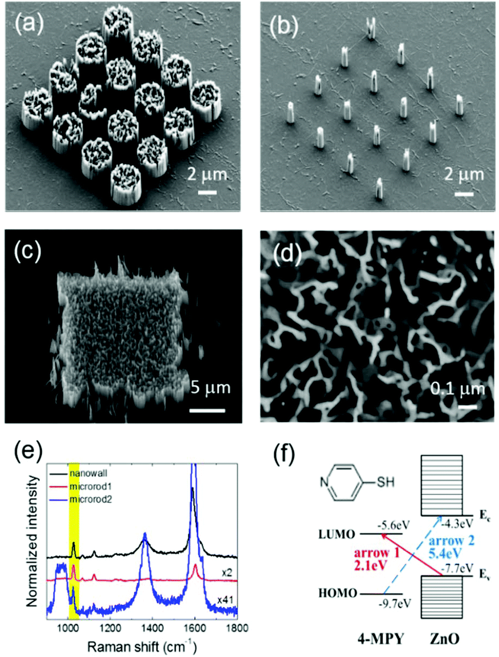 | ||
| Fig. 1 Representative SEM images of ZnO micro/nanostructures grown on CVD-graphene. (a) An ordered array of microrods (rod diameter ∼3 μm). (b) An array of nanotubes (tube diameter ∼400 nm). (c) A square mat with an inner nanowall structure. (d) A magnified view of the nanowall structure. (e) SERS spectra from microrods with different diameters and inner nanowall structures of the mat. Each SERS intensity was multiplied by some factors to show the same magnitude of the 4-MPY Raman peak at 1020 cm−1 marked by a yellow column. (f) Schematic view of energy band alignment between ZnO and 4-MPY (molecular structure is shown) and possible CT transitions (denoted by arrow 1 and arrow 2) depending on the laser excitation. | ||
The scanning electron microscopy (SEM) images in Fig. 1(a), (b), (c), and (d) show the square arrays of highly oriented and ordered ZnO microrods, nanotubes, micromats, and nanowall structures inside the mat, respectively. These types of ZnO nanostructures possess high-quality crystalline properties with little defects and display excellent optical characteristics, as shown in previous reports.23,24 ZnO microrods with large diameters (d ≥ 1000 nm) exhibit maze-like inner wall structures, presumably due to lateral diffusion and crystal growth inside the rod, whereas nanotubes with smaller diameters (d ∼ 100 nm) have void inner structures. These inner wall structures in large-diameter rods are expected to be beneficial for SERS due to the large surface area for molecular adsorption and the roughened surface morphology suitable for generating localized surface plasmon only if the ZnO surface would be coated with metallic films or nanoparticles. SERS data are acquired from the ZnO–graphene substrates as shown in Fig. 1(e) using a 514.5 nm wavelength laser. 10 μl of 10−4 mol L−1 (M) 4-MPY molecules were drop-deposited and naturally dried before performing Raman measurements. By using the Si substrate peak intensity at 520 cm−1 as a reference signal, we can normalize and compare peak intensities from different microrod structures to confirm that a nanowall forest structure gives higher Raman intensity than small-diameter microrod structures. While the overall Raman signal strengths from different microstructures vary, the characteristics of 4-MPY SERS such as peak positions and relative intensities appear quite similar for all the samples, which suggests that CM effects from ZnO materials are universal and reproducible. Note that the surface plasmon frequency of ZnO semiconductors lies in the IR range so EM-related resonance cannot take place in ZnO semiconductors with the visible wavelength laser sources. Previous studies observed similar CM results when 4-MPY was deposited on ZnO.25,26 Wang et al. proposed a CT between the valence band of ZnO and the LUMO level of 4-MPY as a plausible explanation of the SERS, by ruling out other possible factors such as molecular resonance and plasmon resonance.25 Shin et al. also reported a large enhancement of the 4-MPY Raman signal adsorbed on ZnO nanowires and explained that one of the enhancement mechanisms was due to chemical CT.26 In fact, the excitation laser wavelength of 514.5 nm (2.41 eV) used in the study is reasonably close to the energy difference (2.1 eV) between ZnO valence (−7.7 eV from vacuum) and 4-MPY LUMO (−5.6 eV) levels. A schematic explanation of the CT between molecules and the ZnO surface is illustrated in Fig. 1(f).27 We propose that the laser-induced CT from the ZnO VB to the 4-MPY LUMO is a governing factor for strong SERS results, denoted by arrow 1. This polaronic transition corresponds to the so-called “C” term in Herzberg–Teller (H–T) CT contributions.21,28 In contrast, another possible transition from the 4-MPY highest occupied molecular orbital (HOMO) to the ZnO CB corresponding to the “B” term in H–T contributions is very unlikely to happen due to the very large energy gap (∼5.4 eV) for the laser excitation energy to overcome (arrow 2). This is strong experimental evidence that proper positioning of the energy band gaps between the semiconductor surface and adsorbed molecules is important to maximize the resonant CT component for SERS.
In order to verify whether the CT from the semiconductor to molecules is indeed responsible for SERS, we coated the ZnO surface with thin HfO2 layers via an atomic layer deposition (ALD) process and measured the corresponding SERS signals because the thickening of the HfO2 layer may interfere with the CT processes between ZnO and molecules. HfO2 ALD coating on other oxide or metallic substrates has been employed to yield a smooth and uniform surface in the previous studies.29,30 We assume that the SERS signal intensity would be strongly dependent on the amount of electrons moving across the oxide layer because these electrons can affect the dipole polarization in target molecules. In Fig. 2(a), representative SERS results from ZnO rods coated with thin HfO2 layers are presented. A notable signal at 1020 cm−1 (ring-breathing mode) of 4-MPY is observed to decrease as the thickness of the oxide layer increases sufficiently. In Fig. 2(b), the Raman signal is plotted as a function of the oxide thickness or the distance between ZnO and 4-MPY. It is evident that the SERS signal vanishes exponentially as the oxide thickness increases, and it is undetectable as the oxide thickness reaches ∼4 nm, which may be assigned a CT cutoff range for the SERS CM. In order to further understand the CT process in the presence of the thin oxide layer, the characteristic exponential decaying length is estimated in terms of a simple one-dimensional (1D) tunneling formula, where the transmission probability diminishes exponentially as a function of the potential barrier width. A rough estimation of the tunneling distance can be obtained by solving a 1D quantum potential barrier problem.31
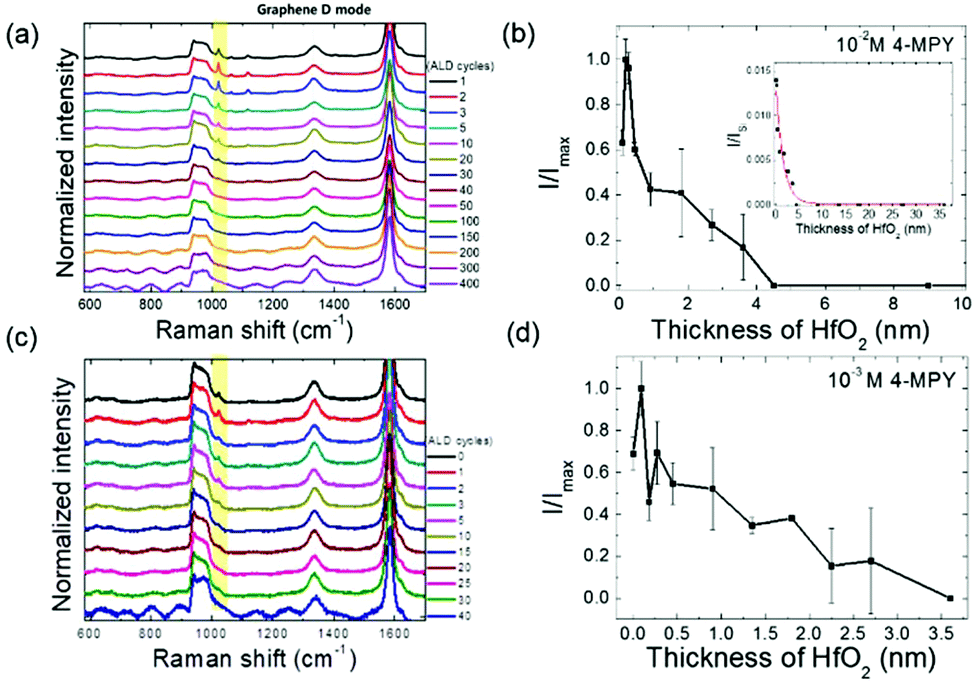 | ||
| Fig. 2 SERS spectra from a ZnO/HfO2/4-MPY system. (a) SERS of 4-MPY (10−2 M concentration) drop-deposited on ZnO coated with various thicknesses of HfO2 layers. The numbers on the right vertical axis indicate the ALD cycle repetition numbers. (b) Normalized intensities at the 1020 cm−1 mode as a function of the HfO2 coating thickness (∼0.9 Å per cycle). The inset denotes an exponential decay of 1020 cm−1 mode intensity (normalized to that of the Si 520 cm−1 mode) over a HfO2 coating thickness of 35 nm. (c) SERS of 4-MPY (10−3 M concentration) using HfO2 coating layers with atomic and nanoscale thicknesses. (d) Normalized peak intensities at 1020 cm−1 as a function of the HfO2 coating layer thickness. Note a significant oscillating behavior of the Raman intensity in the sub-nanometer thickness range. Averaged SERS intensities were obtained from randomly selected several laser spots on the samples. | ||
The exponential decaying length is calculated to be ∼0.1 nm when a potential barrier height of 1 eV and a free electron mass of ∼0.5 MeV are assumed. However, the actual decaying length estimated by the least-squares-regression data fitting over the whole range shown in the inset of Fig. 2(b) is about ∼1.5 nm, which is more than 10 times the calculated value. Note that this big discrepancy between the measured and calculated effective lengths cannot be resolved even if a much smaller effective mass of charge carrier or reduced potential barriers are used for calculation. It should also be noted that the measured cut-off distance (∼4 nm) representing the thickness limit of signal detection is greater than the decaying length (∼1.5 nm) from the exponential data fitting so that we can examine the diminishing Raman signals over the full range of exponential decaying. This result implies that a simple 1D potential barrier description would not be sufficient to reveal the underlying mechanisms of the CT process across the oxide layers.
A clue to reconcile such a large mismatch may be obtained by carefully analyzing the SERS data especially at the subnanometer range of oxide thickness (d < 1 nm). A sign of oscillating behavior of Raman intensity in the subnanometer range in Fig. 2(b) was observed, which looks like the Ramsauer–Townsend effect in quantum tunneling.32 In another set of experiments using 10−3 M concentration of 4-MPY and focusing on the subnanometer oxide thicknesses as displayed in Fig. 2(c) and (d), the oscillating behavior of SERS intensity is even more obvious. Here, we propose that the SERS intensity is maximized whenever the electron transmission probability comes close to unity. According to the quantum wave theory, in the presence of potential barriers or wells, the transmission probability (T) in quantum tunneling can reach the maximum (T = 1) whenever a certain condition (En − V = n2π2ℏ2/2md2, where V is the potential height, n is an integer, m is the electron mass, and d is the potential width) is met. When n = 1 and E1 − V = 1 eV are used for a condition of the transmission peak, the calculated potential width d (i.e., oxide thickness) is ∼0.6 nm, which is compatible with the oxide thickness range where the oscillating behavior of SERS intensity is observed in Fig. 2. In addition to the quantum oscillation, the SERS intensity increases immediately as the HfO2 coating is applied to the ZnO surface. This initial increase of SERS signals may seem unaccountable only if the tunneling electron energy is below the energy band edge of the HfO2 layer. A recent report has proved, however, that the presence of a prebarrier coating layer may actually increase the transmission probability over the uncoated case as long as the electron energy is greater than the prebarrier potential height.33 Remarkably, in the same work, oscillation in transmission probability is also observed when the prebarrier coating thickness varies. Based on all the above analyses, it can be inferred that the prebarrier HfO2 layer may yield a potential well rather than a potential barrier for photo-excited electrons tunneling from ZnO to 4-MPY layers (see Fig. S4 in the ESI†). Ongoing efforts to find detailed energy band alignments and bending at interfaces are expected to confirm our conclusion.
It should be highlighted that this is the first observation that the CT strength changes as a function of the semiconductor–molecule distance in a solid-state environment based on the quantum tunneling process. In this observation, the EM enhancement can be excluded as a possible source of SERS because the surface plasmonic resonance frequency of ZnO is far below the excitation laser frequency, and the surface plasmonic EM field, if any, can easily exceed the length scales of ∼10 nm normal to the surface. Besides the resonant nature of a CT, the nonresonant charge coupling of chemisorbed molecules on the ZnO surface may be considered another source of chemical contributions. If that is the case, however, the SERS signal must diminish significantly as soon as the first HfO2 coating applies to the ZnO surface because 4-MPY molecules cannot make good contact with ZnO to form chemical complexes as long as the thin oxide layer covers the ZnO surface. Thus, the nonresonant charge coupling can also be ruled out for our present SERS result. It is also worth mentioning that the initial increase of the Raman signal at the sub-nanometer coating thickness might be somehow related to the imperfect coverage of HfO2 on the ZnO surface. If that would be true, however, some crucial observations still cannot be understood why Raman molecules attached to the ultrathin HfO2 layer produce stronger signals than the ones on the ZnO surface and why the SERS intensity is oscillating rather than decreasing monotonously with oxide layer thickening.
We also checked whether other types of substances can be detected through CM effects using the ZnO–molecule system. Fig. 3(a) shows the SERS results when 4-aminothiophenol (ATP) instead of 4-MPY is used as Raman probe molecules on ZnO nanostructures. Apparently, no 4-ATP signal was detected except Raman peaks from the underlying graphene and Si substrate, in contrast to the 4-MPY case, which may be understood considering a very large energy gap (∼7 eV) between the LUMO level of 4-ATP and the ZnO VB in comparison with the excitation laser wavelength used (∼2.4 eV). From the band diagram shown in Fig. 3(b), however, the other CT transition from the HOMO of 4-ATP to the ZnO CB might generate SERS signals if a longer wavelength of excitation laser is selected comparable to the transition energy gap of ∼1.4 eV or 886 nm, which needs to be verified in a future study.
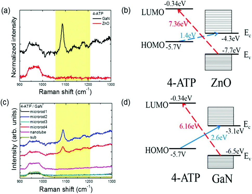 | ||
| Fig. 3 (a) Observed SERS spectra likely due to the transition from 4-ATP HOMO to GaN CB levels. Note that the 4-ATP mode is not visible when the molecules were deposited on ZnO. (b) Energy band diagram from a ZnO/4-ATP system to show possible CT routes. (c) The SERS spectra of 4-ATP from different microrods and nanotubes that have various diameters in the range from 300 nm to 4 μm. The bare substrate is CVD graphene on Si without any nanostructures. (d) Energy band diagram from a GaN/4-ATP system to show possible CT routes. Note that a transition from the 4-ATP HOMO to the GaN CB more likely occurs rather than a transition from the VB to the LUMO band in accordance with the excitation laser wavelength in use. | ||
On the other hand, it was found that 4-ATP signals can be enhanced on GaN substrates, as also shown in Fig. 3(a). It is stimulating to note that the energy levels of GaN are different from those of ZnO and then the GaN CB would be more suitable for CT effects with the HOMO level of 4-ATP molecules as demonstrated in Fig. 3(d). In fact, SERS signals from 4-ATP deposited on GaN microstructures with different diameters are clearly visible in Fig. 3(c), although it is uncertain why some microstructures work better than the others. Yet, the enhancement factor in the 4-ATP and GaN system is calculated to be ∼16.1, which is far smaller than ∼1218.7 in the 4-MPY and ZnO system. We also obtained the SERS spectra from 4-mercaptobenzoic acid (4-MBA) on ZnO, where the energy difference between the 4-MBA HOMO and the ZnO CB is ∼2 eV and that between the 4-MBA LUMO and the ZnO VB is ∼7.3 eV, and got similar results with an enhancement factor of ∼6.0 (see Fig. S3 in the ESI† for spectra. The details of the calculations are also shown in the ESI†). This is additional evidence that enhancement of the Raman signal due to CT is asymmetric: far more efficient enhancement occurs when charges are transferred from the semiconductor VB to the molecular LUMO compared to the other way. These results further support that a resonant CT process plays a critical role in SERS from semiconductor–molecule systems, and it can be inferred that using a specific excitation laser wavelength and semiconductor, some molecules can produce larger SERS signals than the others depending on different transition probabilities between semiconductor energy bands and molecular energy states.
Conclusions
In conclusion, from our report the CT effects on SERS are examined by using ZnO nanostructures/graphene hybrid substrates, and photo-excited electronic tunneling mechanisms are exploited to explain the distance-dependent CT process across thin oxide barriers. The electronic transition from the ZnO VB to the 4-MPY LUMO is primarily responsible for the SERS CM effects, and the relevant CT process is actually proved for the first time. In the combined ZnO/HfO2/4-MPY model system, the characteristic length scale to observe the quantum oscillation is less than 1 nm, whereas the tunneling electrons can reach a much longer distance of ∼5 nm through the oxide barrier, which is a cutoff length scale for the CT process. Our demonstrated ability to detect ballistic charge carriers using sensitive Raman spectroscopy may offer an innovative framework to study not only the SERS CM effects but also a variety of CT phenomena found in engineered nanoscale devices and molecular interfaces abundant in nature.Conflicts of interest
There are no conflicts to declare.Acknowledgements
This work was supported by the Basic Science Research Program (NRF-2016R1D1A1B01009032 and NRF-2018R1A6A1A03025340) through the National Research Foundation of Korea (NRF). This work was also supported by the Global Research Laboratory Program (2015K1A1A2033332) through the NRF funded by the Ministry of Science, ICT, and Future Planning.Notes and references
- M. Fleischmann, P. J. Hendra and A. J. McQuillan, Chem. Phys. Lett., 1974, 26, 163–166 CrossRef CAS.
- D. L. Jeanmaire and R. P. Van Duyne, J. Electroanal. Chem. Interface Electrochem., 1977, 84, 1–20 CrossRef CAS.
- M. Moskovits, Rev. Mod. Phys., 1985, 57, 783–826 CrossRef CAS.
- A. Otto, J. Raman Spectrosc., 1991, 22, 743–752 CrossRef CAS.
- S. Schlucker, Angew. Chem., Int. Ed., 2014, 53, 4756–4795 CrossRef.
- C. Boerigter, U. Aslam and S. Linic, ACS Nano, 2016, 10, 6108–6115 CrossRef CAS.
- J. E. Moore, S. M. Morton and L. Jensen, J. Phys. Chem. Lett., 2012, 3, 2470–2475 CrossRef CAS PubMed.
- S. K. Saikin, Y. Chu, D. Rappoport, K. B. Crozier and A. Aspuru-Guzik, J. Phys. Chem. Lett., 2010, 1, 2740–2746 CrossRef CAS.
- X. X. Han, W. Ji, B. Zhao and Y. Ozaki, Nanoscale, 2017, 9, 4847–4861 RSC.
- X. Wang, W. Shi, G. She and L. Mu, Phys. Chem. Chem. Phys., 2012, 14, 5891–5901 RSC.
- I. Alessandri and J. R. Lombardi, Chem. Rev., 2016, 116, 14921–14981 CrossRef CAS PubMed.
- S. M. Morton and L. Jensen, J. Am. Chem. Soc., 2009, 131, 4090–4098 CrossRef CAS PubMed.
- X. Ling, S. Huang, S. Deng, N. Mao and J. Kong, Acc. Chem. Res., 2015, 48, 1862–1870 CrossRef CAS.
- B. Sharma, R. R. Frontiera, A. Henry, E. Ringe and R. P. Van Duyne, Mater. Today, 2012, 15, 16–25 CrossRef CAS.
- L. Chen, Y. Gao, Y. Cheng, H. Li, Z. Wang, Z. Li and R.-Q. Zhang, Nanoscale, 2016, 8, 4086–4093 RSC.
- L. G. Quagliano, J. Am. Chem. Soc., 2004, 126, 7393–7398 CrossRef CAS PubMed.
- N. Valley, N. Greeneltch, R. P. Van Duyne and G. C. Schatz, J. Phys. Chem. Lett., 2013, 4, 2599–2604 CrossRef CAS.
- S. Hayashi, R. Koh, Y. Ichiyama and K. Yamamoto, Phys. Rev. Lett., 1988, 60, 1085–1088 CrossRef CAS.
- W. Ji, Y. Kitahama, X. Xue, B. Zhao and Y. Ozaki, J. Phys. Chem. C, 2012, 116, 2515–2520 CrossRef CAS.
- B. N. J. Persson, Chem. Phys. Lett., 1981, 82, 561–565 CrossRef CAS.
- J. R. Lombardi and R. L. Birke, J. Chem. Phys., 2007, 126, 244709 CrossRef.
- X. Zhang, Z. Yu, W. Ji, H. Sui, Q. Cong, X. Wang and B. Zhao, J. Phys. Chem. C, 2015, 119, 22439–22444 CrossRef CAS.
- S. I. Park, Y. Tchoe, H. Baek, J. Heo, J. K. Hyun, J. Jo, M. Kim, N. J. Kim and G. C. Yi, APL Mater., 2015, 3, 016103 CrossRef.
- Y. J. Kim, H. Yoo, C. H. Lee, J. B. Park, H. Baek, M. Kim and G. C. Yi, Adv. Mater., 2012, 24, 5565–5569 CrossRef CAS.
- Y. Wang, W. Ruan, J. Zhang, B. Yang, W. Xu, B. Zhao and J. R. Lombardi, J. Raman Spectrosc., 2009, 40, 1072–1077 CrossRef CAS.
- H.-Y. Shin, E.-L. Shim, Y.-J. Choi, J.-H. Park and S. Yoon, Nanoscale, 2014, 6, 14622–14626 RSC.
- J. R. Lombardi and R. L. Birke, J. Chem. Phys., 2012, 136, 144704 CrossRef PubMed.
- J. R. Lombardi, R. L. Birke, T. Lu and J. Xu, J. Chem. Phys., 1986, 84, 4174–4180 CrossRef CAS.
- S. Wang, S. Zou, S. Yang, H. Wu, J. Jia, Y. Li, Z. Zhang, J. Jiang, M. Chu and X. Wang, Sens. Actuators, B, 2018, 265, 539–546 CrossRef CAS.
- H.-L. Lu, M. Yang, Z.-Y. Xie, Y. Geng, Y. Zhang, P.-F. Wang, Q.-Q. Sun, S.-J. Ding and D. W. Zhang, Appl. Phys. Lett., 2014, 104, 161602 CrossRef.
- J. J. Sakurai and J. Napolitano, Modern Quantum Mechanics, Pearson, 2010 Search PubMed.
- A. U. Maheswari, P. C. Prema and S. Shastry, Am. J. Phys., 2010, 78, 412–417 CrossRef.
- Z. C. Zhao and D. R. McKenzie, Sci. Rep., 2017, 7, 12772 CrossRef PubMed.
Footnote |
| † Electronic supplementary information (ESI) available: Additional information including the preparation of HfO2/ZnO nanostructures onto graphene films, SEM images of HfO2 coated ZnO nanostructures with different coating thicknesses, experimental methods, and details of SERS enhancement factor calculations. See DOI: 10.1039/c8nr08389d |
| This journal is © The Royal Society of Chemistry 2019 |