
Direct Z scheme-fashioned photoanode systems consisting of Fe2O3 nanorod arrays and underlying thin Sb2Se3 layers toward enhanced photoelectrochemical water splitting performance†
Aizhen
Liao
ab,
Yong
Zhou
 *abc,
Leixin
Xiao
d,
Chunfeng
Zhang
b,
Congping
Wu
abc,
Adullah M.
Asiri
e,
Min
Xiao
b and
Zhigang
Zou
abdc
*abc,
Leixin
Xiao
d,
Chunfeng
Zhang
b,
Congping
Wu
abc,
Adullah M.
Asiri
e,
Min
Xiao
b and
Zhigang
Zou
abdc
aEco-Materials and Renewable Energy Research Center (ERERC), Jiangsu Key Laboratory for Nano Technology, Nanjing University, Nanjing 210093, China. E-mail: zhouyong1999@nju.edu.cn
bNational Laboratory of Solid State Microstructures, Collaborative Innovation Center of Advanced Microstructures, School of Physics, Nanjing University, Nanjing 210093, P. R. China
cSunlite Ltc, Kunshan Innovation Institute of Nanjing University, Kunshan, Jiangsu 215347, P. R. China
dSchool of Engineering and Applied Science, Nanjing University, Nanjing 210093, P. R. China
eKing Abdulaziz University, Chemistry Department, Faculty of Science, Jeddah 21589, Saudi Arabia
First published on 3rd December 2018
Abstract
An elegant Z-scheme-fashioned photoanode consisting of Fe2O3 nanorod arrays and underlying thin Sb2Se3 layers was rationally constructed. The photocurrent density of the Sb2Se3–Fe2O3 Z-scheme photoanode reached 3.07 mA cm−2 at 1.23 V vs. RHE, three times higher than that of pristine Fe2O3 at 1.03 mA cm−2. An obvious cathodic shift of the photocurrent onset potential of about 200 mV was also observed. The transient photovoltage response demonstrates that the suitable band edges (ECB ∼ −0.4 eV and EVB ∼ 0.8 eV) of Sb2Se3, match well with Fe2O3 (ECB ∼ 0.29 eV and EVB ∼ 2.65 eV), permitting the photoexcited electrons on the conduction band of the Fe2O3 to transfer to the valence band of Sb2Se3, and recombine with the holes therein, thus allowing a high concentration of holes to collect in the Fe2O3 for water oxidation. The transient absorption spectra further corroborate that the built-in electric field in the p–n heterojunction leads to a more effective separation and a longer lifetime of the charge carriers.
Introduction
Solar water splitting in photoelectrochemical (PEC) cells has drawn much attention for sustainable hydrogen production, owing to the limited reserve of fossil fuels and the increasing concern of environmental pollution.1–3 Photoanodes for water oxidation are the rate-limiting step for the PEC overall water splitting efficiency. Hematite (α-Fe2O3), an n-type semiconductor with a suitable narrow band gap (2.2 eV), has emerged as one of the most attractive photoanode candidates because of its low cost, (photo)-electrochemical stability, nontoxicity, and earth-abundance.4–7 However, α-Fe2O3 suffers from sluggish water oxidation kinetics, severe surface recombination, poor lifetimes of carriers, and short hole migration distance.8–10 Great efforts such as surface passivation, nanostructure engineering, selective doping, and oxygen evolution cocatalysts have been made to improve its PEC performance.11–15 However, the α-Fe2O3 photoanode developed so far still shows a lower photocurrent density relative to its theoretical maximum of 12.6 mA cm−2 at 1.23 V versus the reversible hydrogen electrode (vs. RHE) under AM 1.5G illumination (100 mW cm−2).9,16 Obviously, a single Fe2O3 component cannot satisfy the requirement of efficiently steering the spatial separation/transfer of electron–hole pairs for high PEC performance. The conjugation of coupling with other semiconductors has been proven an efficient method for solving the weaknesses above by providing a built-in electric field and optimal transportation path.17 Type II heterostructures have been commonly built, allowing photogenerated electrons (holes) to be transferred from one semiconductor with a higher conduction (lower valence) band (CB) to that with a lower conduction (higher valence) band (VB).18 However, the redox ability of this type of heterojunction is dynamically lowered after charge flowing, compared to individual components.Z-scheme photocatalyst systems by mimicking natural photosynthesis in green plants are designed to employ two semiconductors with one H2 production photocatalyst and one O2 production photocatalyst.19 The Z-scheme semiconductor heterojunction possesses a vectorial charge transfer feature, i.e. the photo-induced electrons on the semiconductor with a lower conduction band (CB) potential will combine with the holes on another semiconductor with a higher valence band (VB) potential, and leave the electrons and holes in reduction-evolving and oxidation-evolving semiconductors, respectively. It simultaneously leads to superior charge separation and perseveration of the strong redox ability of each component.18 A direct Z-scheme free of electron mediators provides energetically favorable band alignment for facile migration of charge across the interface in the heterojunction region. While many α-Fe2O3-based Z-schemes of powder systems have been established, such as with g-C3N4,20–22 scarcely have well-constructed Fe2O3 Z-scheme photoanodes been used for the PEC reaction, especially Fe2O3 nanorod array-based ones, which are beneficial for direct charge transfer to conductive substrates.
Sb2Se3 is a direct band gap (1.0–1.3 eV), low-cost, and p-type semiconductor composed of non-toxic and earth-abundant elements, which possesses wide applications in solar selective and decorative coatings, as well as optical and thermoelectric cooling devices.23,24 Sb2Se3 possesses a high absorption coefficient of 105 cm−1 in the visible range and has been selected as a promising photocathode for water splitting into H2.20,25,26
In this work, a direct Z-scheme-fashioned photoanode consisting of Fe2O3 nanorod arrays and underlying thin Sb2Se3 layers free of electron mediators was for the first time rationally constructed. The photocurrent density of the elegant Sb2Se3–Fe2O3 Z-scheme photoanode reaches 3.07 mA cm−2 at 1.23 V vs. RHE, three times higher than that of pristine Fe2O3 at 1.03 mA cm−2. An obvious cathodic shift of the photocurrent onset potential of about 200 mV is also observed. The transient photovoltage (TPV) response demonstrates that the photoexcited electrons on the CB of the Fe2O3 transfer to the VB of Sb2Se3, and recombine with the holes therein, allowing a high concentration of the holes to be collected in the Fe2O3 for water oxidation. The transient absorption (TA) spectra corroborate that the built-in electric field in the p–n heterojunction leads to a more effective separation and longer lifetimes of the charge carriers. The selection of Sb2Se3 for the construction of the present Z-scheme photoanode system has several advantages: (1) the band edges (ECB ∼ −0.4 eV and EVB ∼ 0.8 eV) of Sb2Se3 match well with Fe2O3 (ECB ∼ 0.29 eV and EVB ∼ 2.65 eV) for the Z-scheme; (2) Sb2Se3 is a promising light-absorbing material with the property of efficient charge separation; (3) the narrow bandgap allows the material to absorb as much as possible near-infrared light, extending the range of the light absorption; (4) Sb2Se3 possesses a much higher hole mobility up to 42 cm2 V−1 s−1 compared to 0.2 cm2 V−1 s−1 of Fe2O3. It allows the holes of Sb2Se3 to move fast and arrive on the interface of the Sb2Se3/Fe2O3 prior to those of Fe2O3 recombining with the electrons of the Fe2O3, thus reducing the intrinsic charge recombination of Fe2O3; (5) Sb2Se3 shows an Ohmic junction with the underlying FTO with a small interface resistance, which allows the electrons from the Sb2Se3/Fe2O3 to smoothly flow to the FTO substrate, in contrast to the high resistance of the pristine Fe2O3 with FTO due to the Schottky junction.
Experimental section
Preparation of the Fe2O3/Sb2Se3 photoanode
The fabrication of the Sb2Se3/Fe2O3 Z-scheme photoanode starts with the deposition of a thin Sb2Se3 layer on a fluorine-doped tin oxide (FTO) substrate through thermal evaporation. The evaporator source is commercially available Sb2Se3 powder (antimony(III) selenide, AR, 99.9%). The details of the process are as follows, the FTO glass (1 cm × 2 cm) was cleaned with deionized (DI) water, acetone, and ethanol, and then was placed a few cm apart from the Sb2Se3 powder, inside a quartz tube. With ∼200 sccm of high-purity Ar gas, the furnace temperature was raised to 550 °C. After 30 min of deposition, the furnace was allowed to cool to room temperature under the argon flow, resulting in a successfully uniform coating of Sb2Se3 on the FTO substrate. FeOOH nanorods were then vertically aligned on the Sb2Se3 nanosheets according to the reported methods by our group. More details were described previously.27 Finally, the Sb2Se3/FeOOH was heated at 550 °C for 120 minutes in Ar atmosphere, and subsequently at 650 °C for 15 min resulting in the formation of Sb2Se3/Fe2O3. As a comparison, the Fe2O3 nanorods were synthesized under the same growth conditions, except for the step of deposition of a thin Sb2Se3 layer on a FTO substrate through thermal evaporation.Sample characterization
A FEI NOVA NanoSEM230 scanning electron microscope is employed to investigate the morphology of the samples. The crystal structure of the samples is identified by X-ray diffraction (XRD) (Ultima III, Rigaku) with Cu Kα radiation (k = 0.154 nm). Transmission electron microscope (TEM) images are taken on a JEM 200CX TEM apparatus. X-ray photoelectron spectroscopy (XPS) is carried out on a Thermo Scientific K-Alpha instrument operating with an unmonochromatized Al Kα X-ray source, and the data are calibrated by the binding energy of the C 1s line at 283.6 eV. A Shimadzu UV-2550 spectrometer equipped with an integrating sphere is used to investigate the absorption properties of the samples. Electrochemical impedance spectroscopic (EIS) curves are measured by a PAR2273 workstation (Princeton Applied Research, USA) under a forward bias of 0.2 V and AM 1.5G illumination. Transient photovoltage (TPV) based on the lock-in amplifier measurement were carried out on a home-made system of Tengfeng Xie's group of Jilin University, which researches the separation and kinetic behaviors of photogenerated charge carriers.28,29 The TPV measurement was performed under the illumination of a 355 nm laser pulse.Photoelectrochemical property measurements
The photoelectrochemical (PEC) performance of the photoanodes is investigated in a three-electrode cell using an electrochemical analyzer (CHI-630D, Shanghai Chenhua) under AM 1.5G illumination. The electrolyte is a 1 M NaOH aqueous solution (pH 13.6). The Fe2O3 sample is used as the working electrode. A Pt foil and a saturated Ag/AgCl electrode are used as the counter and reference electrode. The RHE potential is calculated following the formula VRHE = VAg/AgCl + 0.059 pH + EAg/AgCl, where VRHE is the converted potential versus RHE, and at 25 °C. The active area of the Fe2O3 sample is fixed to 0.28 cm2 using a black mask. A cyclic voltammetry method is adopted with a scan rate of 10 mV s−1.
Results and discussion
The fabrication of the Sb2Se3/Fe2O3 Z-scheme photoanode starts with the deposition of a thin Sb2Se3 layer on a fluorine-doped tin oxide (FTO) substrate through thermal evaporation (Scheme 1). The FeOOH nanorod array was then hydrothermally grown onto the surface of the Sb2Se3/FTO, and subsequently annealed in an inert atmosphere to transfer into Fe2O3. The FE-SEM image from the top view of the FTO/Sb2Se3 film clearly shows the apparent difference of the surface of the FTO substrate before (Fig. 1a) and after (Fig. 1b and Fig. S1a†) deposition of the Sb2Se3. The formed Sb2Se3 layer consists of nanosheet-like particles with full coverage of the FTO substrate. FE-SEM elemental mapping and the EDX spectrum demonstrate the presence of Sb and Se elements (Fig. S2†). The corresponding cross-sectional FE-SEM image reveals the thickness of the Sb2Se3 layer to be approximately 120 nm (Fig. 1c). Fig. 1d and e show the cross-section and top view of the vertical growth of the Fe2O3 nanorods on the surface of the Sb2Se3 layer, respectively. No morphological differences of the Fe2O3 nanorod array were observed between the Sb2Se3/FTO and the FTO (Fig. S1b and S1c†), which indicates that the presence of the Sb2Se3 layer has no effect on the rod-like crystal growth of Fe2O3. Fig. S3† shows the UV-Vis absorption spectra of Sb2Se3, Fe2O3, and the Sb2Se3/Fe2O3 film.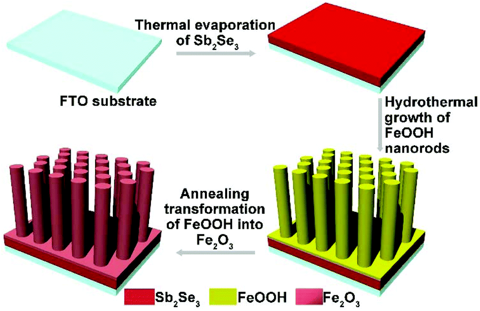 | ||
| Scheme 1 Schematic illustration of the fabrication process of Sb2Se3/Fe2O3. | ||
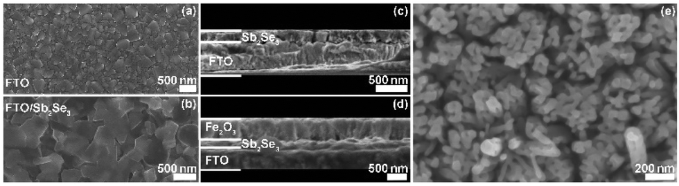 | ||
| Fig. 1 (a) FE-SEM image of FTO. (b and c) Top- and cross-sectional view FE-SEM images of Sb2Se3 with 30 min deposition on the FTO substrate, respectively. (d and e) Cross-sectional and top-view SEM images of Sb2Se3/Fe2O3, respectively. | ||
The XRD patterns clearly show the characteristic diffraction peaks of hematite (Fe2O3; JCPDS 79-0007) and FTO (Fig. S4†). No Sb2Se3 diffraction peaks are identified in the composite film, possibly due to the thinness of the Sb2Se3. The high-resolution XPS profiles of the Sb2Se3 film display the peak positions at binding energies of 530.1 and 538.5 eV, corresponding to Sb 3d5/2 and Sb 3d3/2, respectively (Fig. 2a). The Se 3d spectrum exhibits two peaks of Se 3d5/2 and Se 3d3/2 (Fig. 2b), consistent with Se2− in the case of Sb2Se3.30,31 The Fe 2p high-resolution XPS of both Fe2O3 and the Sb2Se3/Fe2O3 films can be fitted into Fe 2p1/2 and Fe 2p3/2 peaks, centered at binding energies of 723.5 eV and 711.4 eV, respectively, typical values for Fe3+ in Fe2O3.32,33 Satellite peaks at 717.2 eV indexible to Fe2+ were observed in both pristine Fe2O3 and Sb2Se3/Fe2O3, originating from the annealing process-inducing oxygen vacancy (Fig. 2c).34 The O 1s peak can be assigned to two main constituent peaks at 528.9 and 530.4 eV, corresponding to the Fe–O band and OH−, respectively (Fig. 2d).
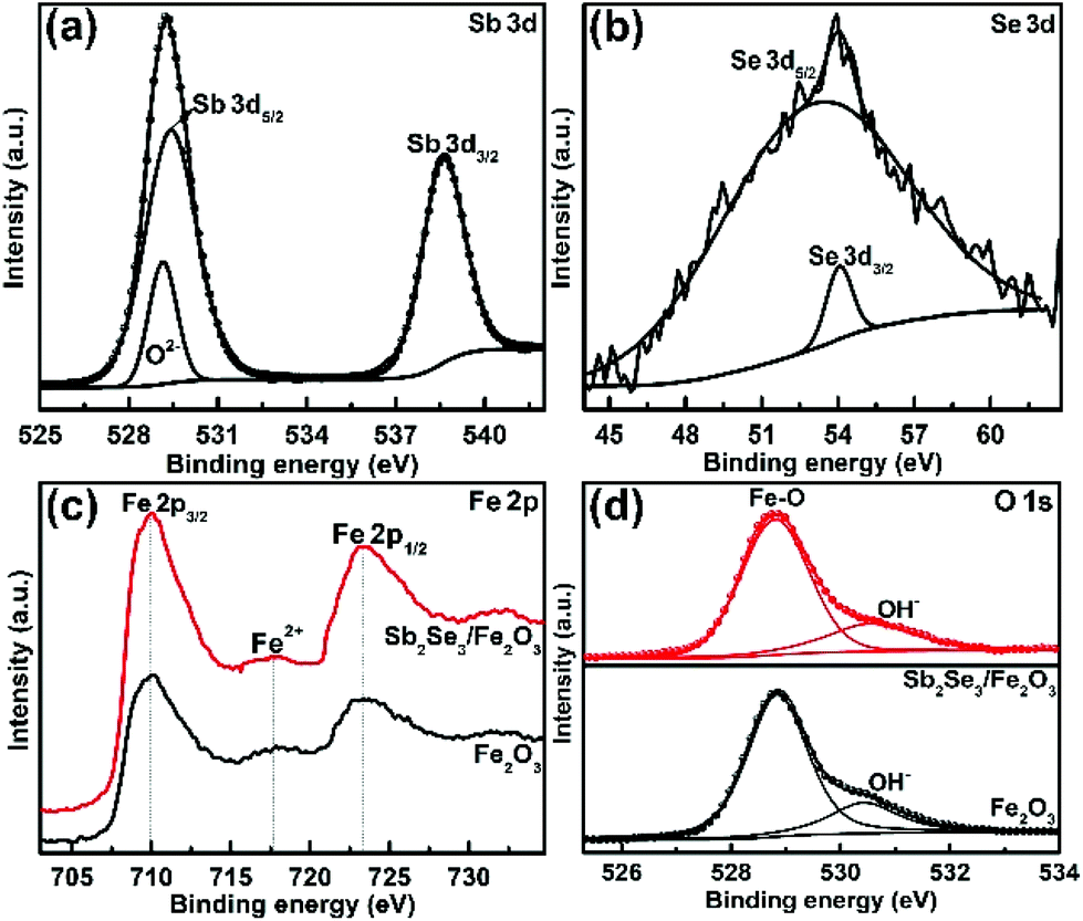 | ||
| Fig. 2 High-resolution XPS (a) Sb 3d, (b) Se 3d signal peak of Sb2Se3, (c) Fe 2p, and (d) O 1s spectra of Fe2O3 and Sb2Se3/Fe2O3. | ||
The PEC performance of the Sb2Se3/Fe2O3 photoanode is dependent on the film thickness of the Sb2Se3 layer (Fig. S5†). 15 min deposition cannot obtain an observable film due to its too thin thickness (Fig. S5b†). It may result in a non-consecutive Sb2Se3 layer, incompletely covering the FTO substrate, and subsequently leading to the reverse reaction, decreasing the PEC performance. 60 and 90 min deposition generates ∼300 nm and ∼500 nm thick Sb2Se3 films (Fig. S5d and S5e†), in which the holes need to move down a long pathway to recombine with the electrons of Fe2O3, also depressing the PEC performance. The Sb2Se3/Fe2O3 with 30 min deposition of about 120 nm thickness exhibits a maximum photocurrent density of 3.03 mA cm−2 at 1.23 V vs. RHE, about three times higher than pristine Fe2O3 (1.09 mA cm−2 at 1.23 V vs. RHE) (Fig. S5c† and Fig. 3a). The corresponding onset potential also obviously cathodically-shifts about 200 mV from 1.00 to 0.80 V. In addition, the Sb2Se3/Fe2O3 photoanode displays a significantly enhanced incident photon-to-current conversion efficiency (IPCE) of 48.5% at 380 nm, double that of pristine Fe2O3 at 22.9% (Fig. 3b). While the Sb2Se3 film alone is a p-type semiconductor which behaves as an insulator under positive bias, the increase of the PEC performance can be ascribed to the unique charge separation mechanism of the Z-scheme system. Furthermore, the Sb2Se3/Fe2O3 photoanode exhibits considerable stability, and the photocurrent only decreased by 12% after 5.6 h of continuous illumination (Fig. S6†).
 | ||
| Fig. 3 (a) Photocurrent–potential (J–V) curves of the Fe2O3 and Sb2Se3/Fe2O3 photoanodes with 30 min deposition of the Sb2Se3 layer under 1 M NaOH (pH ∼ 13.6) aqueous electrolyte under AM 1.5G illumination and in the dark and (b) corresponding IPCE plots obtained and collected at 1.23 V vs. RHE. | ||
The TPV responses for the Sb2Se3/Fe2O3 and Fe2O3 with 355 nm laser illumination were detected with a logarithmical time scale through light illumination from top to bottom electrodes (Fig. 4). The TPV spectra of both photoanodes reveal a positive sign response, implying that the holes move toward and accumulate on the top electrode,34–36i.e. the Fe2O3 side. The Sb2Se3/Fe2O3 displays an almost three-times stronger intensity of TPV signal than the pristine Fe2O3, which can be ascribed to the strong charge carrier separation ability of this structure and high concentration of holes collected in the Fe2O3 with a long surviving time. The Z-scheme mode of the Sb2Se3/Fe2O3 can be schematically illustrated (Fig. 4b). Under light illumination, both Sb2Se3 and Fe2O3 are photoexcited to generate electron–hole pairs. The electrons in the CB of the Fe2O3 shift to the VB of the Sb2Se3 and recombine with the holes therein. The depletion of the electrons of Fe2O3 restrains the intrinsic charge recombination of the Fe2O3, allowing the longer survival time of the holes, which are highly oxidative, and can readily perform oxygen evolution reactions at the electrode/electrolyte interface. Meanwhile, the concentrated electrons in the Sb2Se3 side are highly reductive, which then transfer to the counter electrode to efficiently drive hydrogen production.
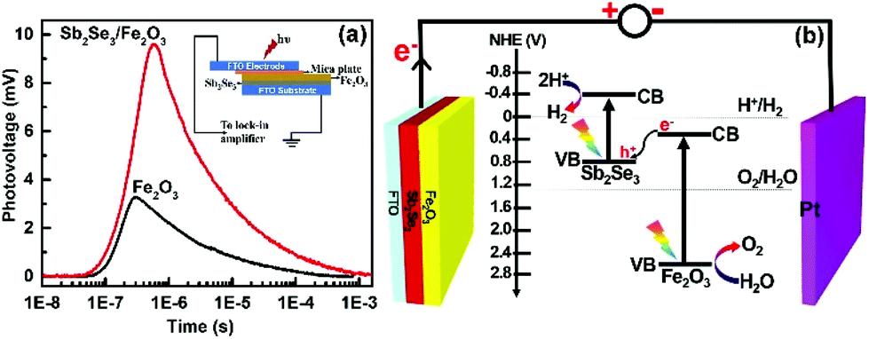 | ||
| Fig. 4 (a) TPV of Fe2O3 and Sb2Se3/Fe2O3. The wavelength and intensity of the excitation pulse are 355 nm and 100 μJ, respectively. Inset: Schematic setup of the TPV measurement. (b) Schematic illustration of the charge transfer on the Sb2Se3/Fe2O3 photoanode. | ||
To explore the impact of Sb2Se3 on the photogenerated charge carrier dynamics, the TA spectra of the pristine Fe2O3 and Sb2Se3/Fe2O3 on a 0–6393 ps time scale were probed after 350 nm laser excitation (Fig. 5a and b). Across the probed wavelength range, both the films display two excited state absorption (ESA) signal peaks, a weak one at ∼500 nm and a strong one at ∼575 nm. Two peaks showing a similar time-decay tendency derive from the absorption of photo-generated holes with different energy levels.37 The ESA signal at the latter was the main spectroscopic feature in the hematite sample, which can be attributed to the absorption of photo-generated holes.38–40 The TA spectrum of Sb2Se3/Fe2O3 exhibits a higher intensity and a slow time-dependent decay rate within the monitored time range, compared with the Fe2O3. It suggests that the Sb2Se3/Fe2O3 possesses more photogenerated holes and a lower recombination rate of carriers, further confirming the Z-scheme structure. The time profiles of the TA probed at 575 nm were fitted by a two-exponential function in Fig. 5c. The Sb2Se3/Fe2O3 shows a relatively slower decay than the Fe2O3 in the 9–18 ps windows, and the lifetimes for the Fe2O3 and Sb2Se3/Fe2O3 were detected 2.1 ps and 3.7 ps, respectively, indicating that the Z-scheme heterostructure is beneficial for separation of the photogenerated charges, and maintaining the separation long enough for the surface reaction of water oxidation. The open-circuit photovoltage (OCPV) calculated from the difference of the open-circuit potentials between dark and illumination reveals that the OCPV values of Sb2Se3/Fe2O3 was higher in comparison with the pristine Fe2O3, additionally demonstrating the improvement of the charge separation efficiency (Fig. S7†).
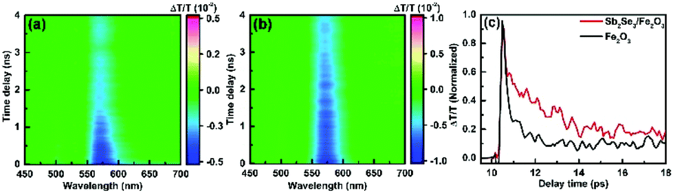 | ||
| Fig. 5 Two-dimensional color maps of the obtained transient absorption data for (a) Fe2O3 and (b) Sb2Se3/Fe2O3. (c) Normalized transient absorption vs. time curves of Fe2O3 and Sb2Se3/Fe2O3 in air atmosphere, λex = 350 nm, at 575 nm. | ||
Solid-state current–voltage (J–V) characterization was conducted. FTO and Ag were used as the front and back contacts, respectively. While the pristine Fe2O3 film displays rectifying characteristics to form a Schottky junction with FTO, the linear J–V feature of the FTO/Sb2Se3 indicates an Ohmic junction formation of the Sb2Se3 with FTO. The steep slope close to that of the FTO implies a small contact resistance at the interface of the Sb2Se3/FTO, which allows the electrons from the Sb2Se3 to smoothly flow to the FTO substrate. The increased slope of the Sb2Se3/Fe2O3 compared with pristine Fe2O3 clearly states that more electrons in the former transfer to the FTO substrate in comparison with the latter. The electrochemical impedance spectroscopy (EIS) semicircle for the Sb2Se3/Fe2O3 photoanode displays a smaller diameter than Fe2O3, also demonstrating that the interface charge transfer rate increases after combination of the thin Sb2Se3 layer (Fig. 6b).
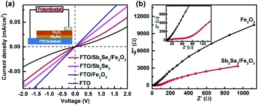 | ||
| Fig. 6 (a) Solid-state J–V characteristics of FTO, FTO/Fe2O3 and FTO/Sb2Se3/Fe2O3. (b) The EIS under AM 1.5G simulated sunlight illumination. | ||
Conclusion
A novel direct Sb2Se3/Fe2O3 Z-scheme system was successfully constructed through a vapor deposition process of a thin layer of Sb2Se3 on a FTO substrate, followed by growth of Fe2O3. The elegant Z-scheme Sb2Se3/Fe2O3 reaches a photocurrent density of 3.03 mA cm−2 at 1.23 V vs. RHE, and shows an extraordinary cathodic shift of the onset potential of about 200 mV. The enhanced PEC performance is ascribed to the unique charge separation and transfer mechanism. This study may not only inspire further development of new direct solid-state Z-scheme systems for solar water splitting with superior performance, but also could be significant in meeting the demands of environmental domains.Conflicts of interest
There are no conflicts to declare.Acknowledgements
This work was supported by 973 Programs (No. 2014CB239302), NSF of China (No. 21773114 and 21473091), NSF of Jiangsu Province (No. BK20171246). Additionally, the TPV measurement was greatly supported by Prof. Tengfeng Xie of Jilin University, China.Notes and references
- M. Gratzel, Nature, 2001, 414, 338–344 CrossRef CAS PubMed.
- M. G. Walter, E. L. Warren, J. R. McKone, S. W. Boettcher, Q. Mi, E. A. Santori and N. S. Lewis, Chem. Rev., 2010, 110, 6446–6473 CrossRef CAS PubMed.
- H. Wang, H. W. Lee, Y. Deng, Z. Lu, P. C. Hsu, Y. Liu, D. Lin and Y. Cui, Nat. Commun., 2015, 6, 7261–7269 CrossRef CAS PubMed.
- A. Fujishima and K. Honda, Nature, 1972, 238, 37–38 CrossRef CAS PubMed.
- H. G. Cha, S. J. Kim, K. J. Lee, M. H. Jung and Y. S. Kang, J. Phys. Chem. C, 2011, 115, 19129–19135 CrossRef CAS.
- J. Y. Zheng, M. J. Kang, G. Song, S. I. Son, S. P. Suh, C. W. Kim and Y. S. Kang, CrystEngComm, 2012, 14, 6957–6961 RSC.
- H. G. Cha, M. J. Kang, I. C. Hwang, H. Kim, K. B. Yoon and Y. S. Kang, Chem. Commun., 2015, 51, 6407–6410 RSC.
- G. Wang, Y. Ling, D. A. Wheeler, K. E. George, K. Horsley, C. Heske, J. Z. Zhang and Y. Li, Nano Lett., 2011, 11, 3503–3509 CrossRef CAS PubMed.
- H. G. Cha, J. Song, H. S. Kim, W. Shin, K. B. Yoon and Y. S. Kang, Chem. Commun., 2011, 47, 2441–2443 RSC.
- T. K. Van, H. G. Cha, C. K. Nguyen, S. W. Kim, M. H. Jung and Y. S. Kang, Cryst. Growth Des., 2012, 12, 862–868 CrossRef CAS.
- Y. Kuang, Q. Jia, H. Nishiyama, T. Yamada, A. Kudo and K. Domen, Adv. Energy Mater., 2016, 6, 1501645–1501652 CrossRef.
- G. Liu, J. Shi, F. Zhang, Z. Chen, J. Han, C. Ding, S. Chen, Z. Wang, H. Han and C. Li, Angew. Chem., Int. Ed., 2014, 53, 7295–7299 CrossRef CAS PubMed.
- G. Liu, S. Ye, P. Yan, F. Xiong, P. Fu, Z. Wang, Z. Chen, J. Shi and C. Li, Energy Environ. Sci., 2016, 9, 1327–1334 RSC.
- Z. Lin, J. Li, Z. Zheng, L. Li, L. Yu, C. Wang and G. Yang, Adv. Energy Mater., 2016, 6, 1600510–1600520 CrossRef.
- F. Le Formal, E. Pastor, S. D. Tilley, C. A. Mesa, S. R. Pendlebury, M. Grätzel and J. R. Durrant, J. Am. Chem. Soc., 2015, 137, 6629–6637 CrossRef CAS PubMed.
- J. Y. Kim, D. H. Youn, K. Kang and J. S. Lee, Angew. Chem., Int. Ed., 2016, 55, 10854–10858 CrossRef CAS PubMed.
- J. Schneider, M. Matsuoka, M. Takeuchi, J. Zhang, Y. Horiuchi, M. Anpo and D. W. Bahnemann, Chem. Rev., 2014, 114, 9919–9986 CrossRef CAS PubMed.
- H. Li, Y. Zhou, W. Tu, J. Ye, Y. Zhou and Z. Zou, Adv. Funct. Mater., 2015, 25, 998–1013 CrossRef CAS.
- H. Li, W. Tu, Y. Zhou and Z. Zou, Adv. Sci., 2016, 3, 1500389–1500391 CrossRef PubMed.
- Z. F. Jiang, W. M. Wan, H. M. Li, S. Q. Yuan, H. J. Zhao and P. K. Wong, Adv. Mater., 2018, 30, 1706108–1706117 CrossRef PubMed.
- X. She, J. Wu, H. Xu, J. Zhong, Y. Wang, Y. Song, K. Nie, Y. Liu, Y. Yang, M.-T. F. Rodrigues, R. Vajtai, J. Lou, D. Du, H. Li and P. M. Ajayan, Adv. Energy Mater., 2017, 7, 1700025–1700032 CrossRef.
- J. Wang, X. Zuo, W. Cai, J. Sun, X. Ge and H. Zhao, Dalton Trans., 2018, 47, 15382–15390 RSC.
- N. S. Platakis and H. C. Gatos, Phys. Status Solidi A, 1972, 13, K1–K4 CrossRef CAS.
- J. Black, E. M. Conwell, L. Sigle and C. W. Spencer, J. Phys. Chem. Solids, 1957, 2, 240–251 CrossRef CAS.
- J. Tan, W. Yang, Y. Oh, H. Lee, J. Park and J. Moon, ACS Appl. Mater. Interfaces, 2018, 10, 10898–10908 CrossRef CAS PubMed.
- L. Zhang, Y. Li, C. Li, Q. Chen, Z. Zhen, X. Jiang, M. Zhong, F. Zhang and H. Zhu, ACS Nano, 2017, 11, 12753–12763 CrossRef CAS PubMed.
- A. Liao, H. He, Z. Fan, G. Xu, L. Li, J. Chen, Q. Han, X. Chen, Y. Zhou and Z. Zou, J. Catal., 2017, 352, 113–119 CrossRef CAS.
- L. Bi, X. Gao, L. Zhang, D. Wang, X. Zou and T. Xie, ChemSusChem, 2018, 11, 276–284 CrossRef CAS PubMed.
- S. Li, L. Hou, L. Zhang, L. Chen, Y. Lin, D. Wang and T. Xie, J. Mater. Chem. A, 2015, 3, 17820–17826 RSC.
- Y. Zhou, M. Leng, Z. Xia, J. Zhong, H. Song, X. Liu, B. Yang, J. Zhang, J. Chen, K. Zhou, J. Han, Y. Cheng and J. Tang, Adv. Electron. Mater., 2014, 4, 1301846–1301854 Search PubMed.
- S. Lu, Y. Zhao, C. Chen, Y. Zhou, D. Li, K. Li, W. Chen, X. Wen, C. Wang, R. Kondrotas, N. Lowe and J. Tang, Adv. Electron. Mater., 2018, 4, 1700329–1700337 CrossRef.
- A. Z. Liao, H. C. He, L. Q. Tang, Y. C. Li, J. Zhang, J. N. Chen, L. Chen, C. F. Zhang, Y. Zhou and Z. G. Zou, ACS Appl. Mater. Interfaces, 2018, 10, 10141–10146 CrossRef CAS PubMed.
- J. J. Deng, X. X. Lv, J. Gao, A. W. Pu, M. Li, X. H. Sun and J. Zhong, Energy Environ. Sci., 2013, 6, 1965–1970 RSC.
- Y. C. Ling, G. M. Wang, H. Y. Wang, Y. Yang and Y. Li, ChemSusChem, 2014, 7, 848–853 CrossRef CAS PubMed.
- H. G. Cha, T. W. Kim and Y. S. Kang, Mater. Lett., 2014, 136, 245–250 CrossRef CAS.
- Q. Bu, S. Li, Q. Wu, L. Bi, Y. Lin, D. Wang, X. Zou and T. Xie, ChemSusChem, 2018, 11, 1–10 CrossRef PubMed.
- K. E. Knowles, M. D. Koch and J. L. Shelton, J. Phys. Chem. C, 2018, 6, 11853–11867 CAS.
- B. Liu, Y. Sun, X. Wang, L. Zhang, D. Wang, Z. Fu and T. Xie, J. Mater. Chem. A, 2015, 3, 4445–4452 RSC.
- M. Forster, R. J. Potter, Y. Ling, Y. Yang, D. R. Klug, Y. Li and A. J. Cowan, Chem. Sci., 2015, 6, 4009–4016 RSC.
- M. Barroso, S. R. Pendlebury, A. J. Cowan and J. R. Durrant, Chem. Sci., 2013, 4, 2724–2734 RSC.
Footnote |
| † Electronic supplementary information (ESI) available. See DOI: 10.1039/c8nr08292h |
| This journal is © The Royal Society of Chemistry 2019 |