
 Open Access Article
 This Open Access Article is licensed under a
 Creative Commons Attribution 3.0 Unported Licence
High performing AgNW transparent conducting electrodes with a sheet resistance of 2.5 Ω Sq−1 based upon a roll-to-roll compatible post-processing technique†
D.
Kumar
a,
V.
Stoichkov
a,
E.
Brousseau
b,
G. C.
Smith
 c and
J.
Kettle
*a
c and
J.
Kettle
*a
aSchool of Electronics, Bangor University, Dean St, Bangor, Gwynedd LL57 1UT, Wales, UK. E-mail: j.kettle@bangor.ac.uk; Fax: +44 (0)1248 382471
bDepartment of Natural Sciences, University of Chester, Thornton Science Park, Chester CH2 4NU, UK
cInstitute of Mechanical and Manufacturing Engineering, Cardiff School of Engineering, Cardiff University, Queen's buildings, The Parade, Cardiff CF24 3AA, UK
First published on 12th February 2019
Abstract
A report of transparent and conducting silver nanowires (AgNWs) that produce remarkable electrical performance, surface planarity and environmental stability is given. This research presents an innovative process that relies on three sequential steps, which are roll-to-roll (R2R) compatible: thermal embossing, infrared sintering and plasma treatment. This process leads to the demonstration of a conductive film with a sheet resistance of 2.5 Ω sq−1 and high transmittance, thus demonstrating the highest reported figure-of-merit in AgNWs to date (FoM = 933). A further benefit of the process is that the surface roughness is substantially reduced compared to traditional AgNW processing techniques. The consideration of the long-term stability is given by developing an accelerated life test process that simultaneously stresses the applied bias and temperature. Regression line fitting shows that a ∼150-times improvement in stability is achieved under ‘normal operational conditions’ when compared to traditionally deposited AgNW films. X-ray photoelectron spectroscopy (XPS) is used to understand the root cause of the improvement in long-term stability, which is related to reduced chemical changes in the AgNWs.
Introduction
The global market in flexible displays, solar energy and large area electronics is expected to boom in the next 5–10 years. For example, a number of market analysts have forecasted the flexible display industry to grow to $30–50bn by 2020 with the rise in next generation e-readers, phones, photovoltaics (PVs) and other flexible displays.1 Other immediate applications exist in touch screens, anti-statics and resistive heaters. The key component of many of these listed applications is a transparent conductor. Thus, the ability to fabricate flexible and transparent conductors is imperative for the success of many such future products. One of the primary current issues to be addressed in this field is that the incumbent technology indium tin oxide (ITO) is not flexible; upon repeated bending, the films are known to crack and lose conductivity, which is particularly prohibitive for future product emergence of flexible displays, electronics and PVs.2–4Metallic nanowires with well-defined dimensions are a promising material for electrical and optical devices, particularly as flexible transparent conducting electrodes (TCEs), and are a strong candidate for ITO substitution.5,6 When deposited from solution processing, they combine several advantages such as high optical transmittance, low sheet resistance (RSH) and mechanical flexibility.4,7–9 These properties make them a candidate for applications such as sensors and detectors, touch screens, flat panel displays, OLEDs, light emitting electrochemical cells (LECs), printed PVs and layers for heated windows.10–12 However, challenges such as long-term environmental stability,13 contact resistance to the active materials,14 high surface roughness, electrical shorting problems and scalable fabrication must be overcome to fully integrate these new electrodes into commercial devices.15 These factors limit a more extensive use of TCE films based on silver nanowires, despite the emergence of companies such as Cambrios (US), C3 Nano (US), Seashell Technology (owned by BASF), and Toppan printing, who are currently offering silver nanowire (AgNW) suspensions.
The optical/electrical properties of AgNW based transparent electrodes depend on a number of factors including the purity of nanowires, geometry, deposition process and post-treatment of samples including hot rolling and thermal annealing.9,16,17 The conductivity relies upon the use of high aspect-ratio NWs to reduce the percolation threshold and thus to obtain a conductive network. By increasing the density of the percolation network, the conductivity can be improved, but this compromises the optical transmittance of the sample.
Post-processing has been used to improve the electrical properties of AgNWs including by annealing, ‘hot rolling’ and rinsing with chemicals that remove impurities such as polyvinylpyrrolidone (PVP).16–22 Currently the best combined electrical/optical performance was reported by Preston et al.,23 who demonstrated a TCE with a transmittance of 91% and a low sheet resistance of 13 Ω sq−1. By considering the trade-off between electrical and optical performance, a figure of merit (FoM) as defined using eqn (1) is often quoted6 which can be calculated for the work of Preston et al. as 300.3. In other work, Andrés et al. have reported a FoM value of 338 without any post-processing of AgNW electrodes with an RSh of 20 Ω sq−1 electrodes and transmittance at 550 nm of 94.7%, prepared by spray deposition.4
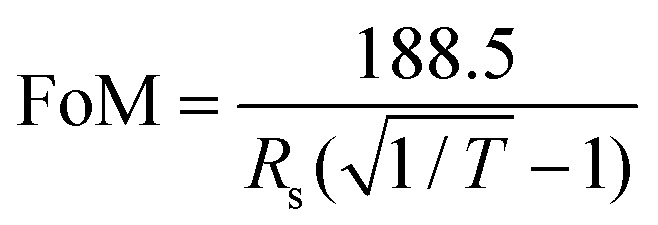 | (1) |
In this work, the application of a roll-to-roll (R2R) compatible post-processing technique is reported which is shown to lead to one of the best reported AgNW electrode performances reported to date. The AgNWs were deposited using spray coating and post-processed using a sequential combination of thermal embossing, sintering and plasma cleaning. The produced films show performances up to RSh = 2.48 Ω sq−1 with transmittances over 85.5% in the visible-SWIR spectrum (300–2000 nm) onto polyethylene naphthalate (PEN) substrates. These result in the highest FoM of 933. Furthermore, the post-processing technique is shown to substantially reduce the surface roughness to a level comparable to that of ITO while also enhancing the stability at elevated temperature and current bias levels, with failure times shown to reduce by two orders of magnitude. The AgNWs are overcoated with ZnO nanoparticles and show significantly reduced surface roughness with excellent thermal stability (∼375 °C) and flexibility while maintaining high electrical conductivity and high optical transmittance. Combining the flexible and conductive films with the scalable roll-to-roll process, we anticipate that the commercial manufacture of a large-scale transparent electrode, replacing ITO, will be realized in the near future.24–26
Experimental
Materials
Silver nanowires (AgNWs) (silver purity: 99.5%, concentration: 20 mg mL−1 in ethanol) were purchased from ACS materials. The average diameter of the AgNWs used was 60 nm and their average length was 20–60 μm. The nanowires were diluted with ethanol to a concentration of 0.4 mg mL−1 prior to spray coating. Flexible transparent substrates of planarised polyethylene-naphthalate (PEN) with a thickness of 125 μm were used for this work and were supplied by DuPont Teijin films in the UK. Zinc oxide (ZnO) nanoparticles were purchased from Sigma-Aldrich and dispersed in 10% ethanol. These had an average diameter of 40 nm, which was verified using TEM measurements. For benchmarking, indium tin oxide (ITO) samples on PET were purchased.Fabrication of AgNW TCEs
Isopropyl alcohol (IPA), ethanol (EtOH) and acetone were used to clean the PEN substrates. For this work, a PMMA buffer layer was spin coated onto the PEN substrates at 2000 rpm followed by annealing at 100 °C for 1 min. AgNW dispersions in ethanol (0.4 mg mL−1) were sonicated for 5 minutes and used just prior to spray coating to ensure that the AgNWs were dispersed in the suspension before spray coating. Spray coating was conducted using a custom-built system with an ultrasonic spray atomiser supplied by MTI in South Korea. The substrates were placed on a substrate heater at 60 °C and the AgNW dispersion was sprayed onto the heated substrates which evaporated the ethanol carrier. The deposition time for preparing the initial electrode film with RSh ≈ 40 Ω sq−1 was 1 min ± 5 seconds. Composite ZnO/AgNW transparent electrodes were manufactured by spray coating nanoparticles onto post-processed AgNWs.Post-processing of AgNW TCEs
In this work three post-processing methods were sequentially applied; thermal embossing, photonic sintering and N2 plasma treatment of electrodes. Fig. 1 shows the fabrication procedure for applying these treatment processes. All three post-processing techniques are undertaken sequentially, but these are all transferable onto a R2R system.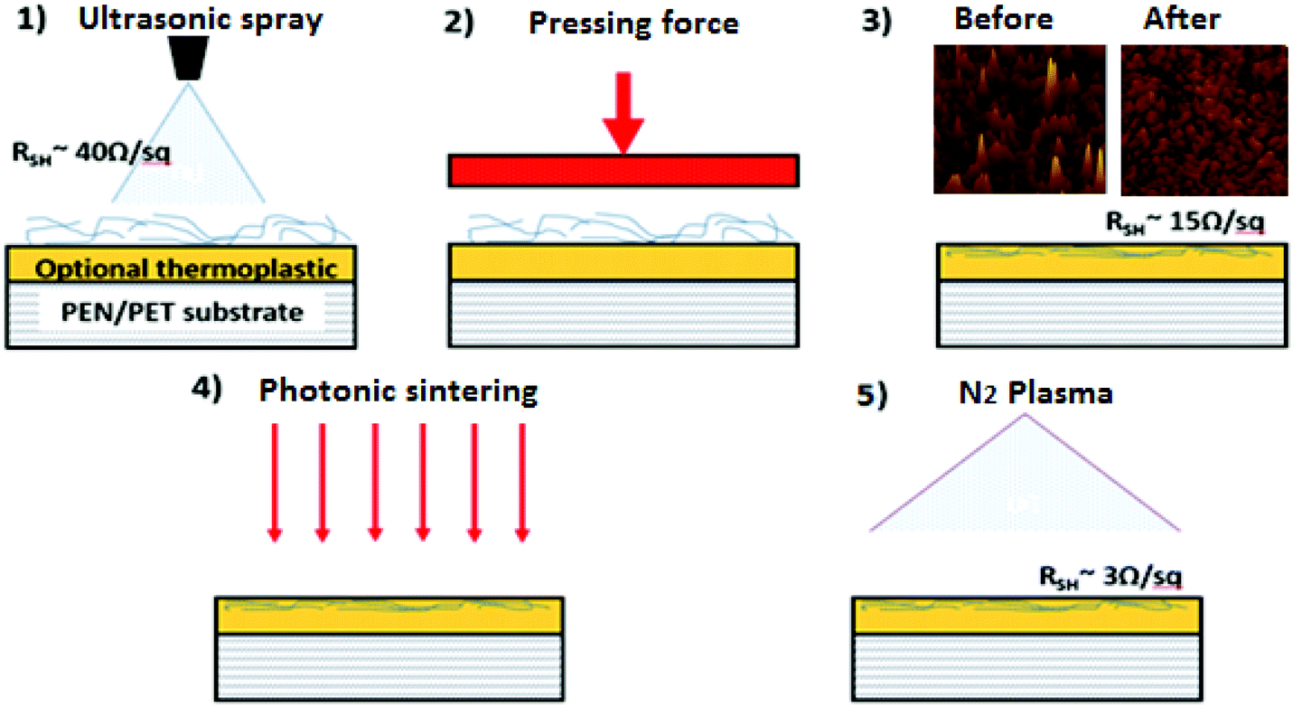 | ||
| Fig. 1 Film deposition and post-processing approach: thermal embossing, photonic sintering, and N2 plasma treatment are used for post-treatment. | ||
Thermal embossing
The AgNW-coated PEN substrates were inserted into a thermal nanoimprint lithography (NIL) system to compress the AgNW on the surface of PEN at different temperatures, times and pressure. The system used was an Obducat 2.5. The thermal-embossing process was conducted using a 2′′ nickel shim, supplied by Nanotypos in Greece, formed from a polished silicon wafer to ensure flatness. The anti-sticking layer BGL-GZ-83 was spin coated onto the nickel shims prior to use in thermal embossing to avoid sticking of the AgNWs and thermoplastic to the nickel shim during the embossing procedure. The nickel shim was cleaned thoroughly in solvents before use. The pressure, time and temperature of the embossing step were all varied, and the process was optimised using the Taguchi Parameter Design method. The optimal conditions found in this way were 5 Bar, 1 minute and 120 °C, respectively. All embossing operations were conducted under ambient pressure rather than under vacuum.Photonic sintering
NIR photonic curing was performed using a Novacentrix system to rapidly anneal the surface for enhanced electrical conductivity. The system was based at the WCPC at Swansea University. Samples were mounted to the system and exposure varied from 450 V, 400 μs to 750 μs with the single energy pulse ranging from 1488 mJ cm−2 to 2712 mJ cm−2. The process ensured that sintering occurred within the top 1 μm of the film surface, rather than the entire thickness of the substrate and therefore impacted mostly upon the AgNW film. By concentrating the sintering so close to the surface, flexible and polymeric substrates can be used, and surface damage can be minimised. The exposure time or energy pulse duration was varied to optimise the lowest sheet resistance. The optimal energy was set at 700 μs with an energy of 2549 mJ cm−2.Plasma cleaning
A plasma treatment step was also applied to AgNW-coated PEN substrates. The AgNW electrodes were nitrogen (N2) plasma treated for 2 minutes, which resulted in the reduction of sheet resistance, although no change in transmittance was noted. The treatment process was conducted using a Diener second ‘Nano’ plasma treatment system at ambient pressure after a 30 seconds nitrogen purge. In this system, a 13.56 MHz RF generator was used at 100 watts power to generate N2 plasma for 120 seconds. Further details of the experimental procedure are provided in ESI-1.†Electrical and optical measurement
The transmittance spectra of silver nanowire electrodes were recorded in the region 350 nm to 1500 nm with PEN as the reference using a HR4000CG-UV-NIR high-resolution spectrometer (Ocean Optics, Inc., USA). The optical haze was measured using a Horiba Scientific Fluoromax-4 spectrofluorometer. In this work, ‘transmittance’, T, is defined as the total transmittance, that is, the sum of direct transmittance, Td, and scattered transmittance, Ts. This enables a value for haze, H, to be defined as eqn (2), which was determined in accordance with ASTM D 1003 standards using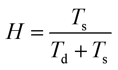 | (2) |
The sheet resistance (RSh) was measured using a four-probe setup (A & M FELL Ltd, UK). The surface roughness was estimated by white light interferometry (WLI) using a MicroXAM surface mapping microscope (KLA Tensor, USA). The roughness was measured in six positions and over two areas (3 × 2 mm) and (0.6 × 0.4 mm), with no discrepancy noted between the measurement areas. The roughness values were averaged across the six areas. Scanning electron microscopy (SEM) images were obtained using a Carl Zeiss 1540XB system equipped with a field-emission SEM.
Manufacture of demonstrator OPVs
To demonstrate the suitability of the AgNW electrode films, inverted Organic Photovoltaics (OPVs) were fabricated onto the developed substrate. To benchmark the AgNW TCEs, PSC devices were also made using ITO coated PET substrates (Rsh = 60 Ω square−1, transmittance = 84%, purchased from Sigma Aldrich) which were first cleaned using deionised water, acetone and isopropanol in an ultrasonic cleaner, and then treated in a UV-ozone reactor with oxygen plasma for 10 minutes. The remaining device fabrication procedure was the same. The AgNW and ITO substrates were coated with ZnO with a film thickness of 80 nm. The samples were transferred into a nitrogen atmosphere glovebox ([O2], <1 ppm; [H2O], <100 ppm), where the active layers and contacts were applied. The absorber was deposited inside the glovebox by spin-coating using the two-step procedure. Active layer BHJ blends using PTB7-Th (as a donor) and [6,6]-phenyl-C71-butyric acid methyl ester (C71-PCBM) (as an acceptor) with weight ratios of 1![[thin space (1/6-em)]](https://www.rsc.org/images/entities/char_2009.gif) :1.5 were prepared and mixed with chlorobenzene solvent with a concentration of 30 mg mL−1. Active layers were applied by spin-casting from a 45 °C solution. The active layer was annealed at 45 °C for 15 minutes before thermal evaporation of the cathode was performed through a shadow mask to define the device area and consisted of 8 nm of MoO3 and 100 nm of silver (Ag) to form the cathode of the device.
:1.5 were prepared and mixed with chlorobenzene solvent with a concentration of 30 mg mL−1. Active layers were applied by spin-casting from a 45 °C solution. The active layer was annealed at 45 °C for 15 minutes before thermal evaporation of the cathode was performed through a shadow mask to define the device area and consisted of 8 nm of MoO3 and 100 nm of silver (Ag) to form the cathode of the device.
The measurement system used to characterize the devices consisted of a Newport solar simulator with 100 mW cm−2 AM1.5G output (calibrated using a silicon reference cell from RERA in the Netherlands). The open circuit voltage (Voc), short-circuit current density (JSC), fill factor (FF) and PCE values are averaged from twelve cells.
Quantitative accelerated lifetime (QALT) of AgNW films
In order to evaluate the long-term effect of post-processing upon the AgNW stability, a bespoke accelerated life testing (ALT) system was constructed. This enabled high current biasing of the AgNW electrodes and repeated sheet resistance calculations every 30 minutes, during which the bias was momentarily switched off (∼5 seconds). In order to accelerate the degradation, samples were placed in an environmental chamber (Weiss UK Ltd). Simultaneous high bias and temperature degradations were conducted at various stress levels, so that the stability could be assessed under ‘normal operation conditions’, which was defined as IBias = 20 mA cm−2 and an ambient temperature of 20 °C (TAMB), which are the typical settings for an OLED or OPV.X-ray photoelectron spectroscopy (XPS) of AgNW films
XPS data were acquired using a bespoke ultra-high vacuum system fitted with a Specs GmbH Phoibos 150 mm mean radius hemispherical analyser with 9-channeltron detection, and an Al Kα twin-anode X-ray source. Survey scans were acquired with 50 eV pass energy, scans over individual photoelectron lines with 15 eV pass energy. Samples were analysed as-received with no further treatment other than removal from the glass supports. Scans were conducted over an area approximately 2 mm in diameter in the centre of the sample. Data were analysed using CasaXPS software version 3.16, with quantification using Scofield cross-sections corrected for the energy-dependence of the analyser transmission and the electron effective mean free paths.Results and discussion
Impact of the post-process technique upon electrical and optical properties
The impact of the individual post-processing techniques and their combined effect are shown in Table 1. It can be seen that the optimised individual processes of thermal embossing, sintering and N2 plasma treatment have a similar effect upon the reduction in RSH, leading to a reduction of ∼50%, when compared to the control samples. By using all three post-processing techniques sequentially, a substantial 93.4% reduction in the sheet resistance could be obtained. Optimisation of the sequence of the different processing steps was conducted and the optimum sequence was (1) NIR sintering, (2) thermal embossing and (3) N2 plasma treatment. Importantly, none of the post-processing techniques showed a compromise in the optical transmittance or the optical haze of the samples with no change observed in these parameters (see Table 1).| Process | R sh (before post-process) Ω sq−1 | R sh (after post-process) Ω sq−1 | Percentage reduction in Rsh (%) | Optical transmittance@550 nm | Optical haze | FoM (after post-process) | Average percentage change in FoM (%) |
|---|---|---|---|---|---|---|---|
| Embossing | 40.4 | 18.1 | 55.2 | 92.9 | 0.2 | 278.9 | 120.8 |
| Sintering | 42.4 | 19.1 | 55.0 | 94.0 | 0.3 | 314.1 | 97.1 |
| N2 plasma | 41.4 | 20.1 | 51.4 | 92.7 | 0.3 | 242.8 | 90.2 |
| Combined | 37.6 | 2.48 | 93.4 | 89.5 | 0.2 | 932.9 | 518.4 |
| Combined and with ZnO NP coating | 37.1 | 2.98 | 81.7 | 85.2 | 0.4 | 758.7 | 498.6 |
| ITO on PET | 40.0 | n/a | n/a | 85.0 | 0.4 | 55.7 | n/a |
| ITO on glass | 12.0 | n/a | n/a | 84.0 | 0.5 | 172.4 | n/a |
The primary reason for the increase in performance after N2 plasma treatment is related to the reduction in the impurity levels (due to the organic impurity of PVP within the AgNW being removed). This is corroborated from the data in the section titled “XPS analysis of the AgNW films”, which shows that the C 1s peak intensity decreases after N2 plasma treatment, indicating a loss of the hydrocarbon content in the AgNW material.
As discussed earlier, a FoM can often be used in transparent conducting electrodes (TCEs) to compare their performances (defined in eqn (1)). The FoM for the combined post-processing technique shows a value of 933; this is substantially higher than the highest reported value in the literature, 338, and represents the best performing TCE based upon AgNWs, or ITO-replacements. As a comparison, the performances are benchmarked against the incumbent technology (ITO) which is reported for both glass and PET substrates (Table 1). In both cases, the AgNW TCEs prepared by the post-processing technique show significantly enhanced performance over the ITO. A typical absorption profile for the AgNW film, which was used for transmission calculations, is shown in ESI-2.†
In the context of transparent conducting electrodes (TCEs), the surface roughness of the sample is important. In OLEDs and OPVs, high surface roughness can lead to AgNWs penetrating through the active regions of the devices leading to electrical shorting. This limits the application of AgNWs in large-area devices or where multiple devices are required. Changes in the surface roughness after post-processing are reported in Table 2. The data show that the root mean square surface roughness (Rq) is reduced to 3.6 nm from 6.4 nm, the average roughness (Ra) is reduced to 2.7 nm from 4.9 nm and the maximum peak-to-valley is reduced to 60.8 nm from 105.9 nm, after the post-processing techniques. The surface roughness can be benchmarked also against incumbent technology (also shown in Table 2) and it is evident that after post-processing, there is 21.5 to 45.4 percent reduction in the Ra, Rq, and Pv surface roughness parameters.
| Sample | R a (before post-process), nm | R a (after post-process), nm | % Change in RA | R q (before post-process), nm | R q (after post-process), nm | % Change in Rq | P V Peak to valley (before post-process nm) | P V Peak to valley (after post-process nm) | % Change in peak to valley PV |
|---|---|---|---|---|---|---|---|---|---|
| AgNWs combined | 6.8 | 3.7 | 45.4 | 8.5 | 4.9 | 43.0 | 101.4 | 79.6 | 21.5 |
| AgNWs and with ZnO NP coating | 4.9 | 2.7 | 44.9 | 6.4 | 3.6 | 43.8 | 105.9 | 60.8 | 42.6 |
| ITO on PET | 3.38 | n/a | n/a | 4.74 | n/a | n/a | 52.2 | n/a | n/a |
| ITO on glass | 1.1 | n/a | n/a | 2.2 | n/a | n/a | 10 | n/a | n/a |
Given the significant enhancements in electrical and surface topographic properties, it is necessary to discuss their origins. SEM images of AgNWs TCEs before and after post-processing are shown in Fig. 2(a) and (b). Based on this, it can be said that the percolating network of AgNWs after embossing possess a more uniform height as the variation in the SEM contrast is less obvious. While topography can be somewhat difficult to evaluate using SEM, the images do show that the embossing step leads to improved physical contact between percolating AgNWs and is therefore likely to increase the number of electrical connections in between AgNWs and the integrity of the contact junctions. As the embossing temperature is low, it is unlikely that there is any ‘fusing’ of AgNW electrodes. The reduction in the SEM contrast indicates reduced secondary electron emission and is likely to be as the AgNWs are partially embedded within the polymer substrate. The embedding of the AgNWs into the polymer surface is likely to contribute to the reduction in the surface roughness as the top surface topography is dominated by the smoothness of the nickel shim which determines the embossed surface smoothness, rather than the protrusions of the AgNWs. In Fig. 2(c), it is apparent that the AgNWs have compressed and are embedded into the PMMA layer and some appear to have fractured during the embossing stage. It is clear that the applied pressure and temperature need to be optimised as over-pressurising during the embossing stage can lead to fractures which will diminish the sheet resistance. The physical changes that occur as a result of photonic sintering are also shown in the SEM image in Fig. 2(c). The data in Table 1 show that the average RSH reduces by ∼50% after sintering. Based on the SEM images, the sintering process affects the AgNW by melting and moderately deforming the AgNW so that the formation of better electrical junctions between individual nanowires is achieved which leads to the enhanced conductivity in films. In previous work, high temperature processing has been shown to remove the residue polyvinyl propyl (PVP) in the AgNWs, leading to improved chemical purity,4,24 which is also likely to contribute to the improvement in the RSH. Because the changes related to N2 plasma treatment are most likely to be changes in the materials chemistry, this is better discussed in section 3.5, where XPS studies of the surface chemistry are discussed. The N2 plasma treatment is likely to also remove the PVP resulting in an improvement in the sheet resistance.
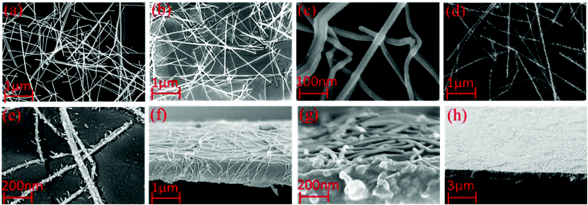 | ||
| Fig. 2 SEM images of (a) AgNWs before embossing, (b) after embossing and (c) after embossing at higher resolution, (d) after embossing and sintering, and (e) after embossing/sintering at higher resolution. Cross-sectional SEM images show AgNWs (f) before embossing, and (g) before embossing at higher resolution and (h) the sample that has been embossed and sintered. | ||
Overcoating of zinc oxide nanoparticles to further improve surface properties
After post-processing, a ZnO nanoparticle dispersion in ethanol was spray coated directly on the post-processed TCEs. The film thickness was measured using cross-sectional SEM, and was found to be 40 ± 3 mm. By spray coating the ZnO nanoparticles, a further planarization layer is deposited onto the AgNW film, without significantly impacting on either RSH or optical transmittance. This is best illustrated in the WLI data shown in Fig. 3, which shows that the surface roughness changes in the control sample, post-processed sample and post-processed sample with ZnO overcoating.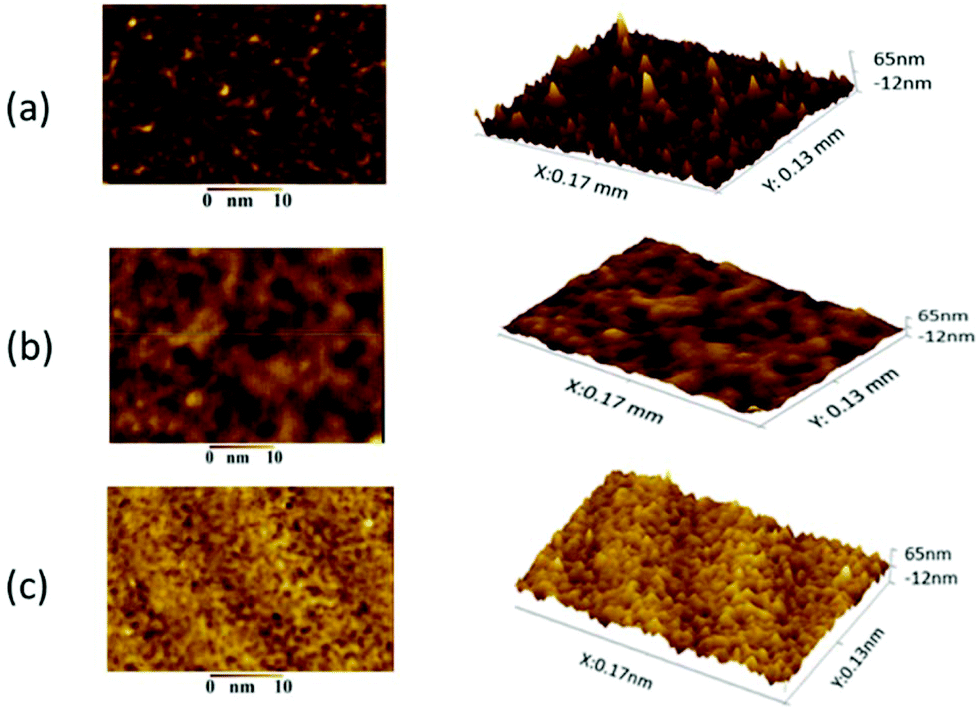 | ||
| Fig. 3 Surface topography images using white light interferometry (WLI): (a) the control sample, (b) post-processed sample and (c) post-processed sample with ZnO overcoating. | ||
The roughness is quantified in Table 2 and the combined AgNW–ZnO electrode is shown to possess a roughness much lower than the control sample and is comparable to ITO on PET. It is clear from the WLI data that the ZnO fills up the voids created by the network of AgNWs and covers any remaining AgNWs that are protruding and thus improves the surface roughness. The result is significant for a second reason; for OPVs and OLEDs, ZnO is often used as an interlayer as the energy levels are favourable for electron extraction or hole injection (for OPVs and OLEDs, respectively). Therefore, the ZnO player has a dual functionality as it planarises the AgNW electrode and ensures energy alignment between the transparent electrode and the active region.
Demonstration of an OPV device
OPVs were fabricated using the procedure discussed in the Experimental section. The performance was benchmarked against an ITO electrode manufactured upon PET. Fig. 4 shows the IV characteristics under AM1.5G illumination from a set of 12 devices made with ITO or AgNW front electrodes, with the remainder of the device structure not changing during these tests. The IV characteristics of the device which were closest to the mean in both sets of devices, the PV performance parameters and manufacturing yield are reported in Table 3.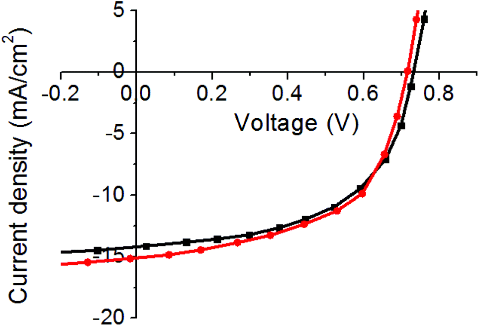 | ||
| Fig. 4 Current–voltage characteristics for the PTB7-Th:PCBM OPV using ITO-based electrodes on PET and glass substrates and a AgNW-based electrode under 100 mW cm−2 AM1.5 illumination. | ||
| V OC (V) | J SC (mA cm−2) | FF | PCE | Yield | |
|---|---|---|---|---|---|
| ITO on PET | 0.732 | −16.3 | 0.56 | 6.70 | 100% |
| AgNWs on PEN | 0.716 | −16.8 | 0.58 | 7.00 | 100% |
In terms of performance, the AgNW shows a moderately improved PV performance; this is primarily due to an increase in the short circuit current density (JSC) of around 0.6 mA cm−2 and a fill factor of 2%, compared to the sample made on an ITO substrate leading to a drop in the PCE. One would expect the AgNW device to have a higher FF than the device made on ITO-PET due to the lower RSH, but the observed differences in the FF are minor. Considering the IV characteristics reported in Fig. 4, the series resistance (RS) of the AgNW device is moderately better than that of the ITO-PET device, but there appears to be a decrease in the shunt resistance (RSH). This decreased Rsh is attributed to the increased shunts and parasitic pathways between AgNW films and the PTB7-Th:PCBM active layer as ZnO might not fully planarise the gap in-between the AgNW and the active layer. In the case of a larger device or modules, the use of AgNWs would have an even greater impact upon PV performance as the RS plays a much more significant role as the area increases. The open circuit voltage (VOC) of the AgNW electrode device is slightly lower as AgNWs possess a lower work-function and this accounts for the observed decrease of VOC.25 In addition to the slight performance increase, the AgNWs do possess a number of additional advantages over ITO including the improved mechanical robustness, no post-treatment requirements and no processing under vacuum.
The device performance has also been tested in resistive heaters and is shown in ESI-4.† The performances were demonstrated for a range of bias conditions, showing that heat can be applied very quickly and over an extended temperature range (limited by the temperature compatibility of the substrate). These data show that the post-processed electrodes can be used for a range of applications.
QALT testing of the reliability of AgNW films
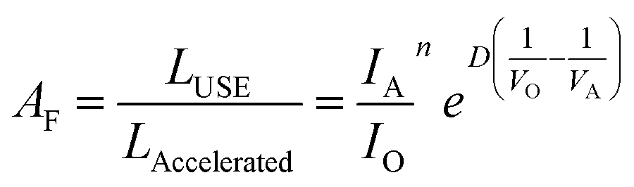
AgNW TCEs are not commonly used in OPVs or OLEDs and therefore substitution of this material into devices requires an assessment of the long-term stability. To achieve this, quantitative accelerated life testing (QALT) can be applied to relate the failure rates achieved at elevated stress levels to what might be observed under normal operational conditions. For this work, four experimental tests were conducted using a (2^2) full factorial experimental design with the following two-stress, two-level conditions; 45 °C/150 mA cm−2, 45 °C/250 mA cm−2, 65 °C/150 mA cm−2 and 65 °C/250 mA cm−2. Given the long lifetime of many TCEs, elevated temperature was applied to accelerate the degradation. When the temperature and current density are the accelerated stresses of a test, then a modified Eyring model can be developed and used as the life test model to relate degradation at an elevated stress level to that at a lower, operational level. This is shown in eqn (3), and is referred to as the temperature–current (TI) relationship. Eqn (3) can be used for predicting life under lower operational conditions, where life is shown as a function of temperature (V) and current density (I) and all other components are fitting parameters and calculation of the acceleration factor (AF) (eqn (4)). Six samples were used under each test condition and a Weibull 2-point distribution was applied for each stress level (defined in eqn (5), where β is defined as the shape parameter, η is the scale parameter, t is the time and f(t) is the probability of failure. Table 4 shows the fitting parameters of the TI model, which have been calculated for the time to increase in resistance by 10% (T10%) and 25% (T25%) of the original value.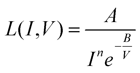 | (3) |
 | (4) |
 | (5) |
| Post-processed T10% | As used T10% | Post-processed T25% | As used T25% | |
|---|---|---|---|---|
| A | 7.79 × 10⁻⁷ | 2.0 × 10⁻⁶ | 9.51 × 10⁻⁸ | 3.20 × 10⁻⁷ |
| B | 9359 | 7824 | 10220 |
8440 |
| n | 1.74 | 1.92 | 1.68 | 1.82 |
| β | 2.47 | 2.08 | 2.42 | 2.11 |
| η | 63353 |
433 | 175002 |
1005 |
To compare the impact of post-processing, a consistent definition of failures is needed. For this work, we calculated the time for 63% of the population of AgNW electrodes tested to show a decline in a particular value [such as 10% increase in resistance (T10%) or 25% increase (T25%)]. This value is often referred to as B(63%). By considering eqn (4), when t = η, the cumulative number of failures in the population, F(t) = 63%; therefore η is equivalent to B(63%).
Based on eqn (3), life is a function of two stress conditions; therefore, life versus temperature and life versus current density can be plotted on a logarithmic scale to show how varying temperature or current density affects the life of the AgNW films, while the other variable is kept constant. This is shown in Fig. 5(a) and (b) for life model fittings from Table 4. The general trend is to be expected; as the stress level of the current density (a) or temperature (b) is increased, the anticipated life of the AgNW film decreases. It is evident from Fig. 5 that the stability of the post-processed samples is substantially higher than that of the non-post-processed samples, by around three orders of magnitude under normal operational conditions (Ibias = 20 mA cm−2 and temperature). This is because the post-processed samples possess a lower resistance due to improved electrical contact. As the power dissipated across the electrode is related to the bias current and resistance as PD = I2·R, the ‘as used’ sample will experience 16× greater power dissipation than the post-processed sample, leading to increased Joule heating, which causes the nanowires to break up and thus create an electrical discontinuity in the nanowire film.14 As more heat is created, the probability of failures increases. Furthermore, during the post-processing procedure, the AgNWs are partially embedded within the underlying polymer, which is likely to act as a barrier layer limiting the impact of oxidation and sulphidisation.
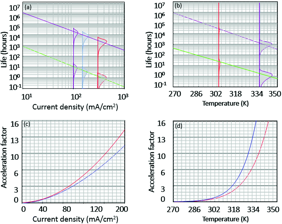 | ||
| Fig. 5 Regression line fitting of the expected time to reach T90% as a function of (a) current density (mA cm−2) and (b) temperature (K) for post-processed and ‘as-used’ AgNW films. Included in (a) and (b) are the fitted probability distribution functions for each stress level. The Acceleration Factor (AF) as a function of the current density and temperature and RH humidity are shown in (c) and (d), respectively. | ||
An important characteristic often assessed in life test models is the acceleration factor (AF), which shows the ratio of the AgNW life at the ‘operational’ stress level to its life at an accelerated stress level and is defined in eqn (3). Both the post-processed and ‘as used’ samples show similar characteristics, but the ‘as used’ samples appears to degrade quicker with increases in the current density.
To evaluate the stability fully, further experiments have been conducted by applying different interlayers onto the AgNW electrodes to observe the interaction between two layers. A single stress condition was applied (Ibias = 300 mA cm−2 and temperature = 65 °C), enabling a relative comparison of stability to be made, which is reported in Fig. 6. The least stable electrode was the ‘as used’ electrode which had no post-processing conducted. The poor stability is due to thermal oxidation of AgNWs as the sample is exposed to the environment. When AgNW films are exposed to air and water, they can be easily oxidized, leading to a sharp increase of the sheet resistance and haze of the AgNW films.26 After the post-processing, the AgNWs are moderately embedded into PMMA and this appears to act as a barrier to inhibit the level of oxidation. By applying a further overcoating the stability is enhanced, although the most significant improvement is obtained by using the ZnO interlayer. The application of PEDOT + DMSO shows the lowest stability as an overcoating layer and is likely to be related to the reactive nature of Ag to environmental S which causes sulfidation.
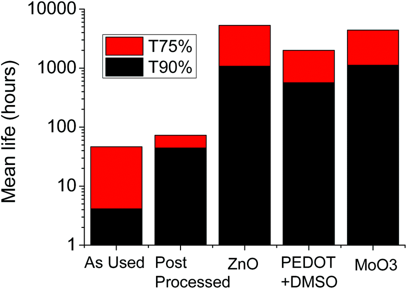 | ||
| Fig. 6 Bar chart showing the mean time to reach T10% (black) and T25% (red) for AgNW films including non-post-processed (‘as used’), post-processed, and post-processed with ZnO, PEDOT:PSS + DMSO and MoO3 transport layers. All samples were tested under the same conditions with a current density of 300 mA cm−2 and a temperature of 60 °C applied. | ||
It is worth noting that the optical properties did not change upon ageing. For example, the optical haze of the aged samples was compared to freshly prepared samples. For samples without any interlayers (i.e. ZnO/PEDOT:PSS), the optical haze of fresh samples was measured at 4.81%, which changed less than ±0.10% after ageing. This was measured from an average of three samples.
XPS analysis of the AgNW films
XPS analysis was conducted on the AgNW films to investigate the impact of embossing, N2 plasma treatment and accelerated ageing on the surface chemistry. Surface compositions as determined by XPS are shown in Table 5, after correction for the presence of small amounts of silicone found as a surface contaminant. All samples showed high levels of C and O, and in most cases relatively strong Ag signals were also observed. All samples also showed low levels of S, Cl and N. The data in Table 5 show the chemical stoichiometry of the different samples. For a deeper analysis, high-resolution scans of the individual photoelectron lines were performed and the curve fitted to known reference data for silver and polymers. In ESI-5,† the curve fitting for C 1s, O 1s, and Ag 3d for all samples is shown.| As prepared | Thermal embossing | N2 plasma treatment | Thermal embossing and N2 plasma treatment | As prepared and aged | Thermal embossing and N2 plasma treatment and aged | |
|---|---|---|---|---|---|---|
| C 1s | 66.66 | 72.92 | 61.73 | 62.31 | 67.42 | 70.95 |
| O 1s | 19.72 | 22.15 | 27.10 | 25.12 | 22.20 | 24.91 |
| Ag 3d | 7.99 | 1.58 | 7.11 | 8.19 | 5.09 | 1.01 |
| S 2p | 1.66 | 0.29 | 1.86 | 2.07 | 2.13 | 0.14 |
| Cl 2p | 1.00 | 0.17 | 0.96 | 0.91 | 0.83 | 0.22 |
| N 1s | 2.97 | 2.89 | 1.24 | 1.40 | 1.79 | 2.32 |
| Na 1s | 0.55 | 0.45 |
The C 1s spectra were typical of those obtained from a poly(methyl methacrylate) PMMA surface, with the hydrocarbon component arising from the backbone and the pendant methyl groups, and the oxygenated components arising from the two carbon–oxygen bonded components of the ester group. The variation in the presence of carbon in this form indicates that there are different levels of AgNW coverage between different samples. Samples that were embossed show higher levels of the carbon surface, indicating that they are submerged in the underlying PMMA.
The levels of Ag did not change significantly upon N2 plasma treatment; however, the embossed samples showed much lower levels of Ag (consistent with the SEM images and carbon XPS data). Nevertheless, even after thermal embossing, Ag was clearly present at the surface, indicating that Ag was not fully embedded into the substrate during this processing step. By comparison, the N2 plasma treated sample showed a decrease in the surface concentration of C and an increase in the surface concentration of O compared to the control. We speculate that the N2 plasma removes hydrocarbon impurities from the AgNW films, namely the PVP used in end-capping during the synthesis, and this leads to the reduction in C and the improved electrical properties. This is supported by the reduction in the surface concentration of N after N2 plasma treatment, which is also likely to be due to the removal of PVP. The increase in the O content after thermal embossing is likely to be because of the raised temperature in ambient air leading to increased oxidation.
On all samples, the Ag 3d5/2 – 3d3/2 doublets were sharp, intense, symmetrical in shape and typically 1.2–1.3 eV in width. In all cases the binding energy of the 3d5/2 component was found in the range 368.8–369.3 eV, somewhat higher than the internationally accepted reference value of 368.27 eV for clean metallic silver.27 In all cases, a doublet separation of 6.02 ± 0.01 eV was found. Ag is unusual among metallic elements in that its oxides tend to exhibit photoelectron peak binding energy shifts to a lower binding energy than the metallic state. Here, a shift to a higher binding energy is seen. This is occasionally seen in the presence of alloying elements, but this cannot be the case here. Instead, it is more likely that the shift is due to charge transfer between the nanowires and the (insulating) PMMA/PEN substrates. This would be consistent with the results reported by Lin & Wang28 and those from other studies of deposited Ag layers. It could alternatively be a function of a more tightly bound crystal structure of Ag in the form of nanowires compared to the bulk metal.
Ageing the as-prepared sample caused small increases in the surface concentrations of O, S and C. Ageing of the post-processed sample caused an increase in the surface concentration of C and small reductions in the surface concentrations of the other elements present, except for Ag where a significant reduction occurred from ∼8% to ∼1%, suggesting the coverage of Ag by a carbon-containing material as a consequence of the ageing process.
S was detected at low levels on all samples, with a possible correlation with the level of Ag (correlation coefficient r2 = 0.79). This is consistent with the reactive nature of Ag to environmental S and the consequent formation of silver sulphides. Inspection of the S 2p photoelectron peaks showed that the majority of S was present in a sulphide state, S2−, consistent with AgS. The thermally embossed and aged samples show low levels of S indicating why these samples remain stable. By ensuring that a greater proportion of the AgNWs are submerged in the underlying PMMA, they remain less susceptible to environmental ageing.
Adhesion and mechanical testing
The AgNW adhesion was determined through a pull-off test using TQC SP302 standard tape (width 1 cm). The procedure followed the ISO 2409 standard which is used for the determination of the adhesion of polymeric layers such as paints and varnish. Considering the AgNW films, no cracks or delamination were observed by visual inspection after the pull-off test which confirmed robust adhesion and compatibility between the PMMA and AgNWs. Measurements of the sheet resistance before and after the pull-off test showed no discernible difference in sheet resistance for the post-processed samples (<5% relative difference). In contrast, for non-processed samples, the sheet resistance increased by 65%, showing that post-processing increases the adhesion of the conductive coating also.We have included bend testing to demonstrate the enhanced mechanical performance of the post-processed AgNW-based electrodes during repeated bending. As shown in ESI-7,† under a 100-cycle test with a bending radius of 20 mm, almost no effect was observed while dramatic failure was observed in the ITO electrode in the same test. The test shows that the mechanical flexibility of the samples is not affected by the post-processing of the AgNW films.
Conclusion
The paper reports the demonstration of high performing AgNW electrodes. High performance was achieved in terms of the low sheet resistance and surface roughness and high long-term stability. The process relies upon three sequential steps: thermal embossing, infrared sintering and a nitrogen plasma treatment. This process leads to the demonstration of a conductive film with a sheet resistance of 2.5 Ω sq−1 and 85% transmittance, thus demonstrating the highest reported figure-of-merit in AgNWs to date (FoM = 933). A further benefit of the processes is that the surface roughness is substantially reduced compared to traditional AgNW techniques. Accelerated life testing has been applied to show that the process leads to enhanced long-term stability in AgNW films. X-ray photoelectron spectroscopy (XPS) is used to understand the improvement in long-term stability. The overall properties of the transparent electrodes developed show an enhancement over the incumbent technology, ITO. Furthermore, the significant improvements in performance demonstrate a significant margin of safety able to withstand further price pressures from ITO in the short to medium term.Conflicts of interest
There are no conflicts to declare.Acknowledgements
This work was supported by the UK Engineering and Physical Sciences Research Council through the EPSRC Centre for Innovative Manufacturing in Large Area Electronics (grant number EP/K03099X/1). The work was also supported by the Solar Photovoltaic Academic Research Consortium II (SPARC II) project, gratefully funded by WEFO. We would like to thank Jeremy Davis of Semitronics and Nocacentrix for their administrative and technical assistance with photonic sintering and to Dr Chris Philips of the WCPC, Swansea University for his help with photonic sintering.References
- A. Anand, Flexible Electronics and Materials Market 2018 Production Value, Gross Margin Analysis, Development Strategy, Future Plans and Comprehensive Research Study Till 2022, http://www.crossroadstoday.com/story/37326055/flexible-electronics-and-materials-market-2018.
- J. Lee, S. T. Connor, Y. Cui, P. Peumans, J. Lee, S. T. Connor, Y. Cui and P. Peumans, Nano Lett., 2008, 8, 689–692 CrossRef CAS PubMed
.
- T. Tokuno, M. Nogi, M. Karakawa, J. Jiu, T. T. Nge and Y. Aso, Fabrication of Silver Nanowire Transparent Electrodes at, Nano Res., 2011, 4, 1215–1222 CrossRef CAS
- L. José Andrés, M. Fe Menéndez, D. Gómez, A. Luisa Martínez, N. Bristow, J. Paul Kettle, A. Menéndez and B. Ruiz, Nanotechnology, 2015, 26, 265201 CrossRef PubMed
- J. H. Cho, D. J. Kang, N. Su Jang, K. H. Kim, P. Won, S. H. Ko and J. M. Kim, ACS Appl. Mater. Interfaces, 2017, 9, 40905–40913 CrossRef CAS PubMed
- H. Sohn, S. Kim, W. Shin, J. M. Lee, H. Lee, D. Yun, K. Moon, I. T. Han, C. Kwak and S. Hwang, ACS Appl. Mater. Interfaces, 2018, 10, 2688–2700 CrossRef CAS PubMed
- J. Ajuria, I. Ugarte, W. Cambarau, I. Etxebarria, R. Tena-Zaera and R. Pacios, Sol. Energy Mater. Sol. Cells, 2012, 102, 148–152 CrossRef CAS
- G. Benatto, a. B. Roth, M. Corazza, R. R. Sondergaard, S. A. Gevorgyan, M. Jorgensen and F. C. Krebs, Nanoscale, 2016, 8, 318–326 RSC
- C. F. Guo and Z. Ren, Biochem. Pharmacol., 2015, 18, 143–154 CAS
- D. Leem, A. Edwards, M. Faist, J. Nelson, D. D. C. Bradley, J. C. De Mello and A. Nws, Adv. Mater., 2011, 23, 4371–4375 CrossRef CAS PubMed
- Z. Ding, V. Stoichkov, M. Horie, E. Brousseau and J. Kettle, Sol. Energy Mater. Sol. Cells, 2016, 157, 305–311 CrossRef CAS
- C. Celle, C. Mayousse, E. Moreau, H. Basti and A. Carella, Nano Res., 2012, 5, 427–433 CrossRef CAS
- J. L. Elechiguerra, L. Larios-Lopez, C. Liu, D. Garcia-Gutierrez, A. Camacho-Bragado and M. J. Yacaman, Chem. Mater., 2005, 17, 6042–6052 CrossRef CAS
- H. H. Khaligh and I. A. Goldthorpe, Nanoscale Res. Lett., 2013, 8, 2–7 CrossRef PubMed
- C. Mayousse, C. Celle, A. Fraczkiewicz and J. Simonato, Nanoscale, 2015, 7, 2107–2115 RSC
- D. P. Langley, M. Lagrange, G. Giusti, C. Jiménez, Y. Bréchet and N. D. Nguyen, Nanoscale, 2014, 6, 13535–13543 RSC
- H. H. Khaligh and I. A. Goldthorpe, Nanoscale Res. Lett., 2014, 9, 1–5 CrossRef PubMed
- D. Diesing, J. Berndt, D. Douai and J. Winter, Thin Solid Films, 2002, 409, 243–247 CrossRef CAS
- Y. Song, J. Chen, J. Wu and T. Zhang, J. Nanosci. Nanotechnol., 2014, 2014, 1–7 Search PubMed
- S. Zhu, Y. Gao, B. Hu, J. Li, J. Su and Z. Fan, Nanotechnology, 2013, 24, 1–7 Search PubMed
- J. Jiu, T. Sugahara, M. Nogi, T. Araki, K. Suganuma, H. Uchida and K. Shinozaki, Nanoscale, 2013, 5, 11820–11828 RSC
- J. Li, Y. Tao, S. Chen, H. Li, P. Chen, M. Wei, H. Wang and K. Li, Sci. Rep., 2017, 7, 1–9 CrossRef PubMed
- C. Preston, Z. Fang, J. Murray, H. Zhu, J. Dai, J. N. Munday and L. Hu, J. Mater. Chem. C, 2014, 2, 1248–1254 RSC
- X. Hu, L. Chen, Y. Zhang, Q. Hu, J. Yang and Y. Chen, Chem. Mater., 2014, 26, 6293–6302 CrossRef CAS
- X. Meng, X. Hu, X. Yang, J. Yin, Q. Wang, L. Huang, Z. Yu, T. Hu, L. Tan, W. Zhou and Y. Chen, ACS Appl. Mater. Interfaces, 2018, 10, 8917–8925 CrossRef CAS PubMed
- X. Hu, X. Meng, J. Xiong, Z. Huang, X. Yang, L. Tan and Y. Chen, Adv. Mater. Technol., 2017, 2, 1700138 CrossRef
- M. P. Seah, I. S. Gilmore and G. Beamson, Surf. Interface Anal., 1998, 26, 642–649 CrossRef CAS
- X. Lin and S. Wang, Indian J. Chem., 2005, 44A, 1016–1018 CAS
Footnote |
| † Electronic supplementary information (ESI) available. See DOI: 10.1039/c8nr07974a |
| This journal is © The Royal Society of Chemistry 2019 |