
 Open Access Article
 This Open Access Article is licensed under a Creative Commons Attribution-Non Commercial 3.0 Unported Licence
Plasmonically-powered hot carrier induced modulation of light emission in a two-dimensional GaAs semiconductor quantum well†
Eric
Ashalley
 a,
Karol
Gryczynski
b,
Zhiming
Wang
*a,
Gregory
Salamo
c and
Arup
Neogi
*b
a,
Karol
Gryczynski
b,
Zhiming
Wang
*a,
Gregory
Salamo
c and
Arup
Neogi
*b
aInstitute of Fundamental and Frontier Sciences, University of Electronic Science and Technology of China, Chengdu, 610054, China. E-mail: zhmwang@gmail.com
bDepartment of Physics, University of North Texas, Denton, Texas 76203, USA. E-mail: Arup.Neogi@unt.edu
cDepartment of Physics, University of Arkansas, Fayetteville, Arkansas, USA
First published on 10th December 2018
Abstract
A hot-electron-enabled route to controlling light with dissipative loss compensation in semiconductor quantum light emitters has been realized for tunable quantum optoelectronic devices via a two-species plasmon system. The dual species nano-plasmonic system is achieved by combining UV-plasmonic gallium metal nanoparticles (GaNPs) with visible-plasmonic gold metal nanoparticles (AuNPs) on a near-infrared two-dimensional GaAs/AlGaAs quantum well emitter. It has been demonstrated that while hot carrier-powered charge-transfer processes can result in semiconductor doping and increased optical absorption, photo-generated carrier density in the quantum well can also be modulated by off-resonant plasmonic interaction without thermal dissipation. Merging these essential emitter-friendly optical characteristics in the two-species plasmon system, we effectively modulate the frequency of the emitted light. The wavelength of the emitted light is tuned by the plasmonically powered hot electron process induced by the AuNPs with a 10-fold emission enhancement induced by the GaNPs. The additional plasmonic element provides functionality to achieving an active plasmonic light emitter that is otherwise far from reach with conventional single plasmonic material-based semiconductors.
1 Introduction
Hot electrons generated from the resonant excitation of the collective oscillation of conduction band electrons in metal and semiconductor nanostructures are essential for a wide range of applications as a variety of effects can be stimulated.1 Photoexcited hot electrons can induce photoemission,2–4 local heating in plasmonic metals,5 photo-desorption of small surface molecules,6 electrical doping of two-dimensional materials,7–9 internal conversion with counter-electrodes10,11 and structurally tunable photochemistry.12,13 As a result, a number of optical processes benefit from hot-carrier induced effects towards more efficient photocatalysis,14–16 photodetectors17 and broadband solar cells though with a few fundamental limitations.18 Plasmonic excitation of metal nanoparticles (NPs) deposited on semiconductor surfaces generates enhanced local field which extensively alters the photoluminescence (PL) and absorption characteristics through the coupling of the recombining carriers to the surface plasmons.19,20 The generated hot electrons from the plasmon-induced process may transfer into the semiconductor to modulate the carrier density. Hot electron induced carrier modulation, as a dynamic process, may hence result in the doping or carrier photo-injection into the semiconductor21 for a broad range of applications including optically configurable transistors.22 Plasmon induced hot electron generation from single Au nanoparticles(AuNPs) has been used to dope and control both the photoluminescence and optical absorption in monolayer MoS2 supported by the confinement in the two-dimensional material.23 Also, a single-nanoparticle plasmonic electro-optic MoS2-based modulator has been designed where the narrow MoS2 exciton coupling with broad Au plasmons yielded gate-dependent deep Fano resonance.24However, due to the nonradiative nature of hot electron induced processes, resonant excitation of plasmons leads to localized and collective plasmon-induced heat dissipation which is detrimental for light emitters or optical modulators.25 Plasmon induced thermally activated nonradiative processes in semiconductor quantum wells (QWs) lead to a decrease in emission efficiency. It is due to the loss of effective carriers for radiative recombination, band-bending and carrier screening resulting in a lower recombination rate. The presence of intrinsic (ohmic) losses in plasmonic systems also limits the achievable local field factor and surface plasmon polariton propagation distance.26 As recently reported, in hot carrier devices, plasmon excitation does not influence the electronic processes. Rather, the carrier transport processes and the metal-dielectric band offset dictate hot carrier photocurrent distribution.27 This is because in noble metals such as Au and Ag the s and d bands regulate the hot carrier energy distribution and mean free path.28 Indeed, electron–phonon interaction controls the hot carrier energy loss and transport. The dissipative loss can be avoided by using off-resonant plasmonic interaction at metal–semiconductor interfaces such as for Ga NPs on GaAs/AlGaAs hybrid single quantum wells (SQWs) which results in enhanced PL emission.29 In this case, the associated electrostatic Stark effect results in blue shifted emission compared to the bare semiconductor SQW. As a result, the carrier density modulation due to off-resonant interaction of the metal NPs with the photons generated within the emitter dominates the recombination process in the absence of strong resonant plasmonic excitation. The electrostatic force induced by off-resonant metal NPs on electrons or holes in a semiconductor is a long-range effect compared to the exponentially decaying plasmonic field.
However, being a relatively slower process than the plasmonically powered process, the electrostatic effect is usually dominated by plasmonic interaction under resonant conditions. It is plausible to harness the fast response of the localized surface plasmon (LSP) induced hot carriers to control light emission30 with single metal nanoparticle plasmonic systems. However, extreme restrains must be exercised on the metal nanoparticle concentration. A higher concentration of metal nanoparticles around a plasmonic emitter can be detrimental to the plasmonically enhanced light emission process as the plasmon frequency can be detuned away from the light emission energy.31 Moreover, single-species metal nanoparticle plasmon systems have one specific bandwidth of plasmon frequency. The presence of an additional plasmon species to a plasmonic light emitter can enable the stimulation of hot carrier generation and photoexcited carrier density modulation. This can be achieved by an optical field resonant to one of the LSP modes in the two-species plasmon system comprised of distinct LSP modes.
Here, we employ a two-species plasmon system tapping into hot carrier and image charge induced hybrid effects to modulate emitted light in a single semiconductor quantum well emitter. These plasmonic NPs when excited with a source that is resonant in energy to the plasmon frequency of one species result in hot carrier generation, but if excited with a higher energy light source off-resonant to the LSP result in carrier density modulation in the semiconductor without dissipative loss.32 We demonstrate that the hot-carrier electron transfer due to resonant pumping of AuNPs can change the frequency of emitted light in the GaAs/AlGaAs quantum well, while the PL intensity is amplified from the image charge effect induced by the GaNPs. We also establish that the angle of incidence and excitation power of the laser influence the coupling between the plasmonic metal nanoparticles and the substrate. The electromagnetic field distribution, absorption spectra and extinction cross sections are calculated via a 3D finite element method (FEM).
2 Results and discussion
The samples were fabricated by depositing a 500 nm GaAs buffer layer and a 20 nm thick Al0.33Ga0.67 layer, followed by the growth of a single GaAs layer with a width of 10 nm, bound by a barrier of 10 nm Al0.33Ga0.67As. The single GaAs/AlGaAs quantum well was capped with a 5 nm layer of GaAs, followed by the deposition of Ga and the formation of Ga droplets at a substrate temperature of 550 °C with the arsenic source being fully closed. After growth, the surface morphology of the QDP samples was characterized using AFM under ambient conditions and the structural properties of the samples were characterized by TEM. Fig. 1a shows the schematic of the GaNPs/GaAs structure. Fig. 1b shows the AFM image of the epitaxially grown GaAs bulk epilayer with Ga nanodroplets (GaNPs). Local field enhancement influences the absorption and emission characteristics. Generally, the field intensity around, at the periphery and the Ga-NPs/substrate contact interface symmetrically increases with decreasing energy and even more so at the localized plasmon energy. Fig. 1c illustrates the electric field distribution at selected energies viewed from the top of the cap layer and absorption calculations due to GaNPs. The color bar applies to all field distribution calculations. We observe a plasmon peak in the visible region close to the 550 nm wavelength. Fig. 1c shows that the LSP energy of the UV plasmon mode in the GaNPs is red-shifted to the visible region with a peak at 2.3 eV due to the high dielectric constant of the substrate (GaAs). The increased electric-field intensity at the higher energy is due to plasmon hotspots originating from the upper UV plasmon mode in Ga.33–35 The d-shell configuration of Ga induces plasmon modes in the UV frequency as well as in the near-IR frequency range.34,36 Nearer to the absorption peak, the field intensity steadily increases in the near-IR range. Resonantly exciting the plasmons close to the plasmon energy induces hot electron generation. The generated hot electrons in turn induce a red shift of the PL emission relative to the bare GaAs substrate. Fig. 1d compares the PL emission from the bare GaAs with and without the GaNPs. The valley and peak refer to the spatial location of the NSOM tip on a GaAs sample with Ga nanodroplets. The valley is the position when the tip is located in between two metal GaNPs, whereas the peak refers to the emission from a position of the tip located on the Ga nanodroplet. Due to dissipation from the hot carrier effect, a slight quenching of the PL emission is observed in the far-field emission profile. A comparison of the near-field PL intensity from a GaAs sample with GaNPs around and away from the GaNPs also demonstrates a PL emission red-shift due to hot electron transfer to the GaAs substrate. Fig. 1e compares the near-field PL emission away from the GaNP(valley) and around the GaNP(peak).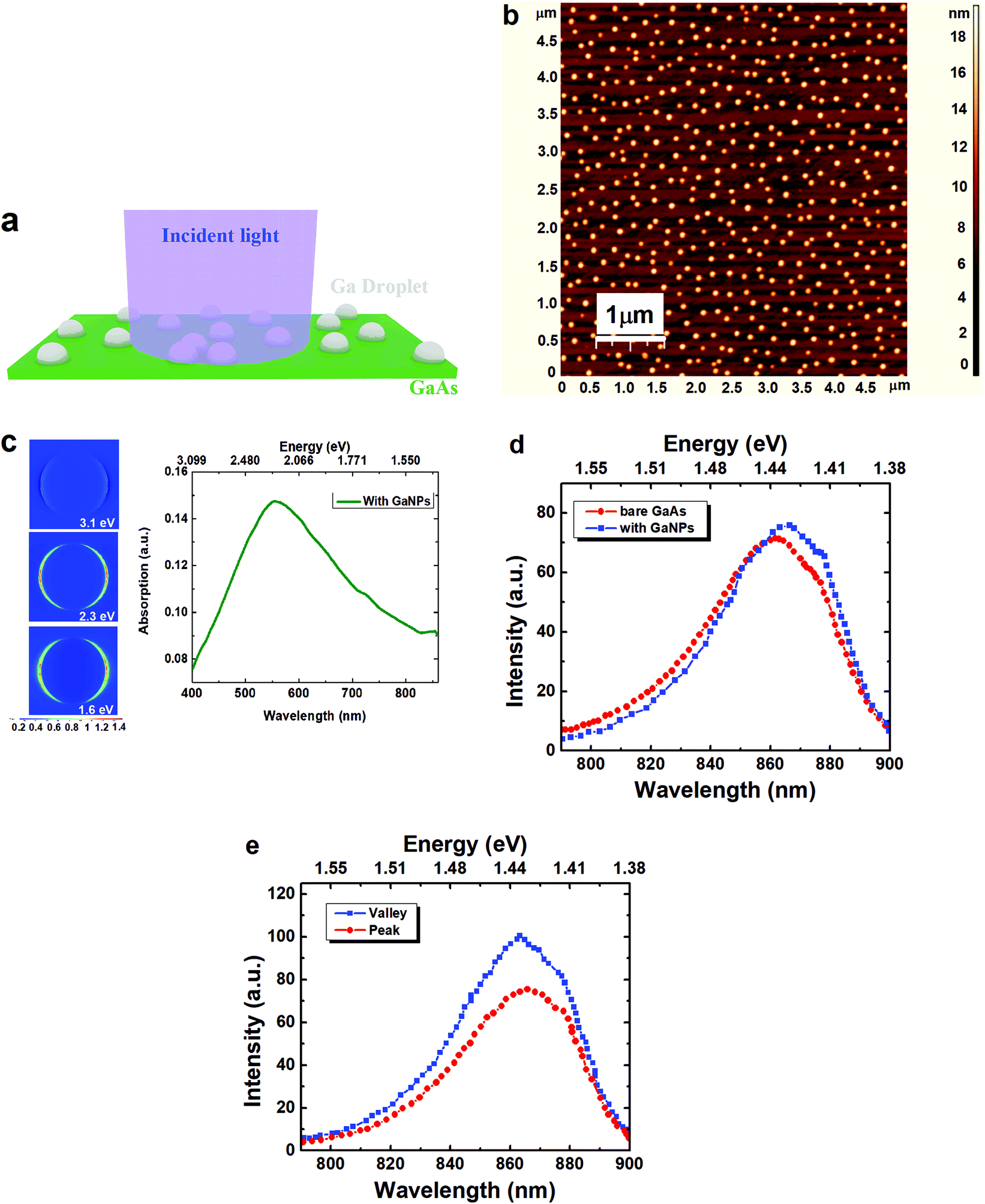 | ||
| Fig. 1 Hot carrier effect due to GaNPs on GaAs upon illumination with a 535 nm excitation laser. (a) A schematic of the the GaNPs/GaAs structure and (b) AFM image of the epitaxially grown GaAs bulk epilayer with Ga nanodroplets. (c) Simulated electric field distribution at 3.1 eV, 2.3 eV and 1.6 eV around the plasmonic GaNPs on the GaAs substrate with corresponding absorption in the visible range at θ = 0 incidence. Here, we observed a visible plasmon peak in the GaNPs/GaAs structure (d) Comparison of the PL emission from bare GaAs with (blue color) and without (red color) GaNPs. (e) Near-field PL emission comparison away from the GaNP(valley) and around the GaNP(peak) from the GaAs sample with GaNPs. Both (d) and (e) respectively illustrate a red shift of the emission due to hot electron transfer to the GaAs substrate in the presence of GaNPs. | ||
To reduce the dissipative loss due to resonant plasmons induced by the hot carriers in the single species plasmon system and increase the strength of optical transition, a two-dimensional quantum confined structure was considered as the emitter. A GaAs dielectric layer was introduced between the metal nanoparticles and AlGaAs/GaAs single quantum well (SQW) emitter. Fig. 2a shows a TEM image showing a 60 nm diameter Ga nanodroplet and details of the GaAs/AlGaAs SQW structure. Fig. 2b shows the AFM image showing the distribution of the nanoparticle sizes. The bare GaAs/AlGaAs SQW which is lattice matched to GaAs emits at 1.53 eV. By exciting these off-resonantly to both the emission of the GaAs/AlGaAs QW and the LSP of Ga with a 1.9 eV laser, the hot carrier effect is avoided. However, due to the carrier density increase around the metal nanoparticles due to the image-charge effect, the PL emission is enhanced about 25 fold. The PL emission is shifted to 1.557 eV owing to the electrostatic image charge effect30 by virtue of the modified radiative recombination. This induces modification of the emitted light as illustrated in Fig. 2c. This modification in radiative recombination is relatively slow owing to the drift and diffusion process involved in the electrostatic attraction of the carriers to the nanoparticle.30 The modified band-line up the quantum well due to the image charge effect is shown in the inset of Fig. 2c. The bandstructure (1) is the quantum well wavefunction for a symmetric GaAs QW. However, in the presence of the GaNPs, the attraction of the electron and hole leads to the electrostatic effect which results in an image charge induced Stark effect.29,31 As the image charge results in a Coulomb attraction of the carriers, the force of the attraction depends on the location of the charge carriers with respect to its distance from the metal nanoparticles. It results in a modification of the alignment of the conduction band and valence band line-up with respect to the spatial distance along the z-direction (growth direction) due to its difference in the distance from the Ga nanodroplet surface. This effect results in an asymmetric bandstructure profile as shown in bandstructure (2) in the inset of Fig. 2c, resulting in a longer PL lifetime as reported earlier30 and also depicted in Fig. 4d. To modulate the carrier density affecting the recombination process, we design an additional recombination channel via the plasmon induced charge transfer process, or exciton–plasmon coupling.
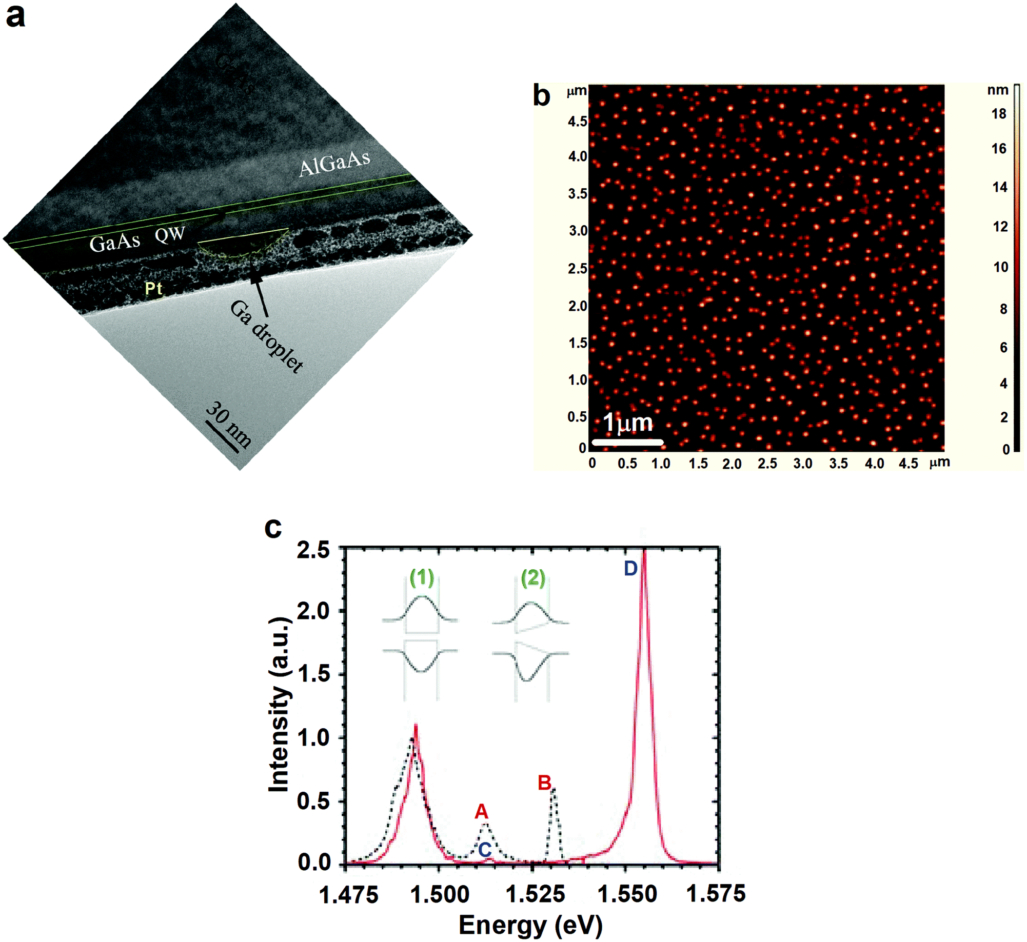 | ||
| Fig. 2 Light emission modulation with off-resonantly excited GaNPs on GaAs SQW at 633 nm. (a) TEM image of a GaAs/AlGaAs SQW with a Ga droplet on the GaAs SQW. The Pt layer was used for the electron microscopy for better conductivity of the electrons and was not present during the optical characterization. (b) AFM image of GaNPs on GaAs SQW (c) Modification of light emission from single GaAs QW due to GaNPs. Peaks A and B correspond to the emission from bare GaAs and GaAs SQW, respectively. Peaks C and D correspond to the emission from bare GaAs with GaNPs and GaAs SQW with GaNPs, respectively. The inset in (c) illustrates the modification in the GaAs quantum well without and with the GaNPs. | ||
AuNPs were deposited together with the GaNPs on the GaAs monolayer to constitute a two-species plasmon system. The AuNPs in colloidal form without any shell layer were dispersed on the surface of the GaAs substrate using a spin-coating technique. Fig. 3a shows the schematic of the two-species plasmon hybrid structure. Fig. 3b shows the AFM images of the GaAs/AlGaAs SQW with high density GaNPs and AuNPs. The AuNP sizes are averagely 120 nm in diameter. In effect, the exciton dipole oscillatory strength depends on the separation distance between the metal and the active layer as well as the exciton Bohr radius of the quantum well. In the two species plasmon system, hot electron generation is induced only when resonantly exciting the surface plasmon resonance in a specific constituent plasmonic metal NP. Such resonant plasmonic interaction in the AuNPs leads to hot carrier generation and increased carrier density. The generated high density hot electrons do not only modify the electronic charge density on the semiconductor surface but also the carrier transport within the single quantum well with Ga NPs on the surface. Hot electron induced electron transfer from Au NPs can result in charge transfer to the GaAs cap layer23,37 that will dope the semiconductor with excess electrons. The Schottky barrier height is drastically lowered at the Au–GaAs interface especially at the measurement temperature (10 K).38 Both the charge transfer and the doping of the GaAs layer can induce screening of the electrons accumulating from the off-resonant interaction, as electrostatically attracted carriers drift and diffuse towards the Ga NPs. The laser excitation energy and intensity can be used to modulate the carrier density which can then be used to tune the emission energy in the hybrid system. To better understand the plasmonic coupling in the two-species plasmon system, we model the field distribution of the two resonant plasmonic systems comprising GaNPs and AuNPs on the GaAs cap layer by solving the Maxwell's frequency dependent electromagnetic wave equations in the form
 | (1) |
| σext = σabs + σsca | (2) |
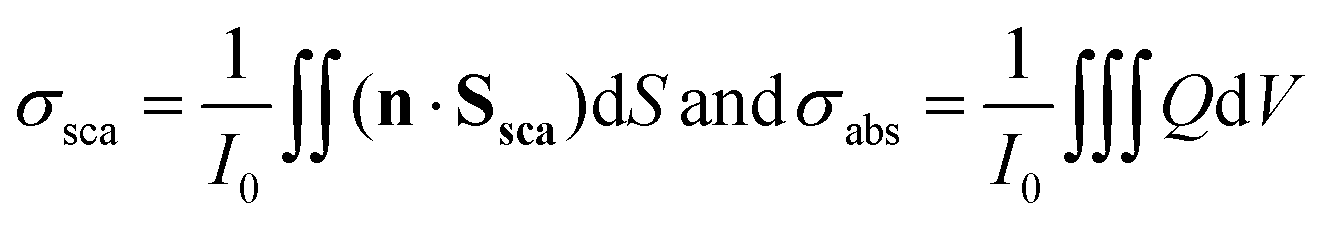
n is the normal vector pointing outwards, Ssca is the scattered intensity vector, I0 is the incident intensity and Q is the power loss density in the particles. Fig. 3c compares the absorption of the GaAs/GaNPs (in Fig. 1c) to that of GaAs/AuNPs/GaNPs on a 10 nm thick GaAs cap layer at normal incidence. Huge enhancement in the electric field and increased absorption are recorded in the presence of the AuNPs compared to the single GaNPs species case due to plasmonic coupling between the two species. At 45° incidence however, an additional peak emerges below the emission energy. Fig. 3d compares the extinction cross section calculation for the single species and dual species plasmon systems on the 10 nm thick GaAs cap layer at 45° incident angle. Peak A corresponds to the plasmon frequency of the single species system. The peak B corresponds to the plasmon energy in the dual species plasmon case. This additional peak arises from the modification of the plasmon mode energies. In the neighborhood of dielectric substrates, the energy of the plasmon modes of a metallic nanoparticle is modified and lifts the degeneracy of the dipole plasmon modes aligned parallel and perpendicular to the substrate resulting in a substrate permittivity dependent energy splitting.42 So that for the GaAs substrate with a dielectric constant of approximately 12, the interaction is sufficiently strong to induce an energy split. Peak C corresponds to the emission from the GaAs QW due to the added AuNPs. Peak D is in the neighborhood of the GaAs donor–acceptor pair emission.43As a test case, we calculate the extinction cross section for the case of the Quartz and GaN substrate in an identical simulation environment. It is observed that due to its high dielectric constant, the energy splitting occurs only in GaAs (see the ESI†).
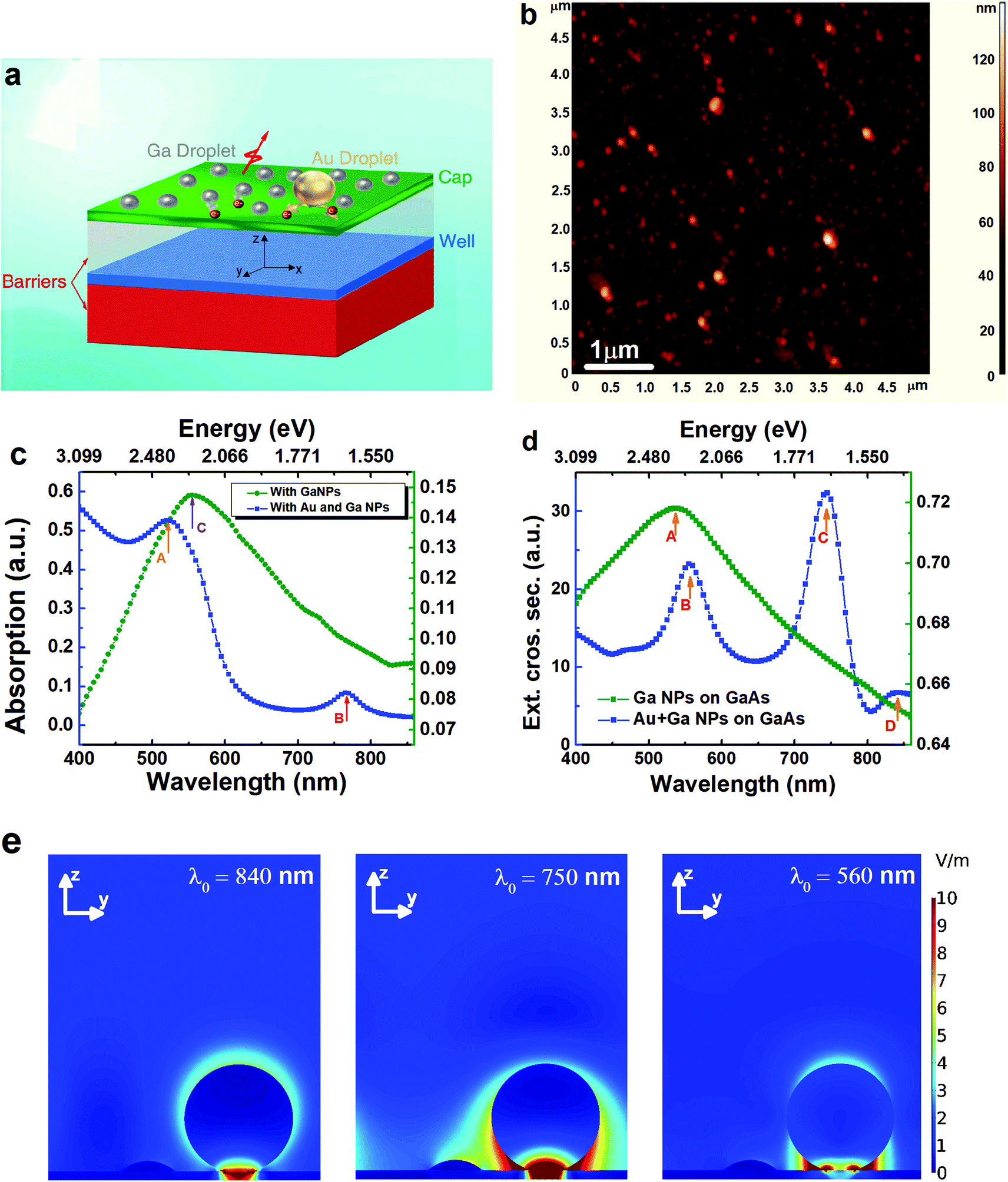 | ||
| Fig. 3 Off-resonant plasmonic interaction due to both GaNPs and AuNPs on GaAs/AlGaAs SQWs. (a) Schematic of the GaNPs and AuNPs on GaAs SQW. (b) AFM image of the GaNPs and AuNPs on the GaAs SQW. (c) Calculated absorption due to GaNPs (green) and due to both Au and Ga NPs (blue) on a 10 nm thick GaAs substrate at normal incidence and 2.3 eV excitation. Peaks A and B correspond to the excitation and emission energies, respectively. Peak C is repeated from Fig. 1c for comparison. (d) Extinction cross section comparison between the single species and two species plasmon systems revealing the resonances in the two systems at 45° incidence. (e) Electromagnetic field distribution at the three plasmonic resonances with a yz cut plane through the centres of the nanoparticles. | ||
The nanoparticle plasmon couples only to its image of surface charges screened by a factor of (ε − 1)/(ε + 1), where ε is the permittivity of the substrate. This is ascribed to the weak metallic nanoparticle–substrate interaction. The electric field intensity at the plasmon frequency increases for incident angles from 15–45 degrees. The field changes and peak shifts can be explained by the relationship between the tangential field and normal field components.44 In the single species plasmon system, although the laser energy is above the band gap of the GaAs, the low photon density originating from the thin GaAs substrate limits its absorption capacity. As such, only localized plasmons due to the GaNPs are present. The extinction peak of the single species plasmon system is therefore independent of the laser incident angle. In the two species plasmon system however, due to the presence of the AuNPs which has plasmon frequency above the GaAs bandgap, a strong local electric field is created especially at the plasmonic resonances (see Fig. 3e). The photon density resulting from the strong local electric field is therefore high enough to cause increased absorption by the GaAs substrate. This breeds a visible GaAs resonance peak which is maximum at an optimum incident angle of 45°. The incident angle has a dipolar dependence based on the position of the AuNPs. As a result, a blue shift in the extinction peak due to the GaAs substrate as a function of the incident angle is observed. See the ESI† for incident angle calculations.
Due to the plasmonically driven hot carrier induced screening,45 holes are pulled towards the high-density surface hot electrons resulting in electron transfer in the GaAs SQW. Fig. 4a describes the hot electron-QW electron/hole interaction leading to changes in the SQW band gap and subsequent red shifting of the emission as a result of the dominant hot carrier induced effect. Here, the blue and red arrows represent the electron–hole attraction and repulsion interaction. In the single plasmon case, there is increased carrier concentration around the GaNPs. In addition to the accumulated carriers, the larger AuNPs induce screening and photocarrier excitation.
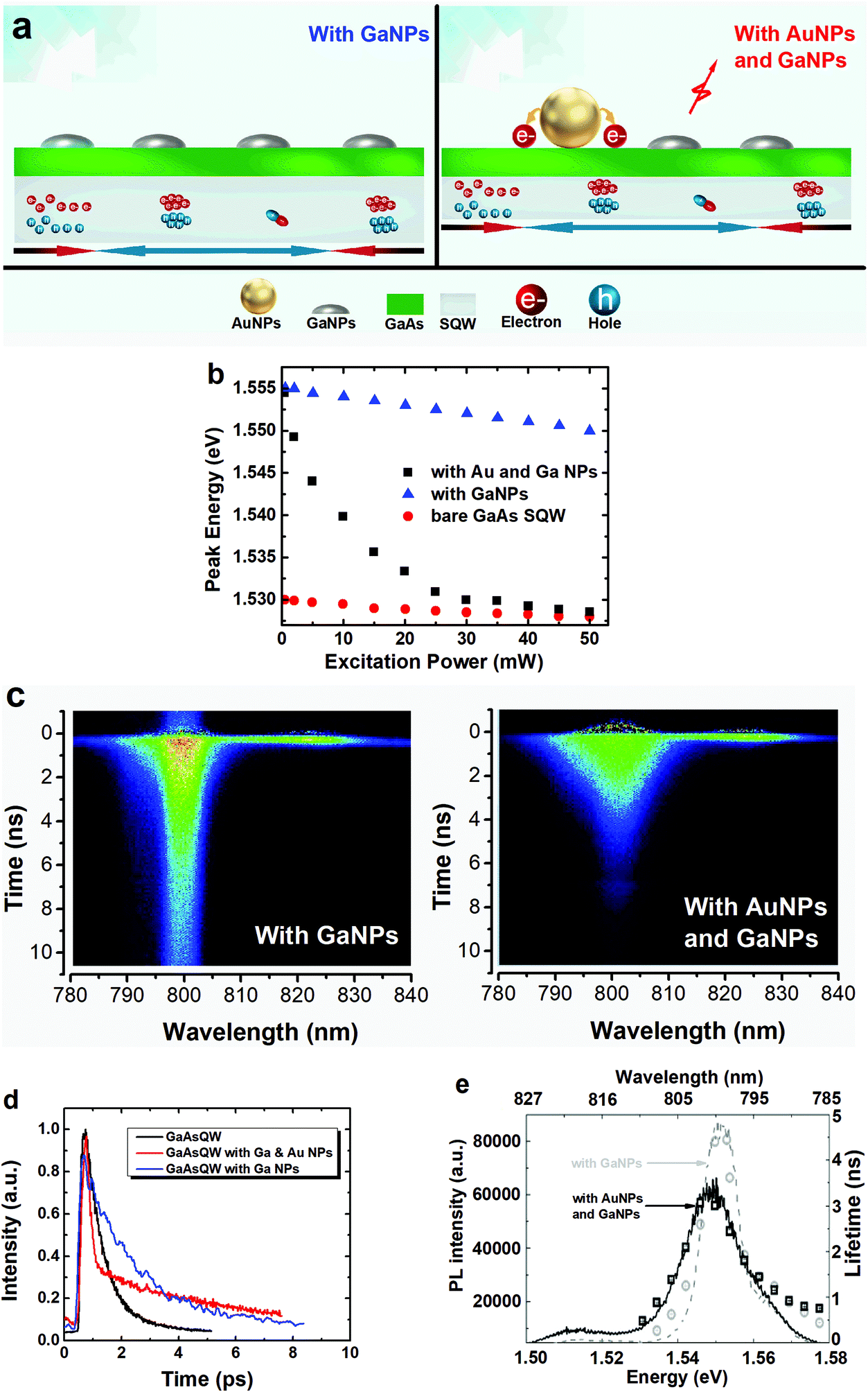 | ||
| Fig. 4 Light emission tuning due to the presence of both hot carrier and image charge induced effects. (a) Schematic describing the surface hot electron-QW electron/hole interaction. (b) Excitation power dependent PL energy tunability. (c) Time-resolved measurement of the PL emission lifetime with GaNPs and with both AuNPs and GaNPs showing shorter overall lifetime in the presence of AuNPs. (d) PL emission decay time comparison between the GaAs QW, GaAs QW with Ga NPs and GaAs QW with Ga and Au NPs. (e) A comparison of the photoluminescence recombination lifetime along with the PL emission intensity due to GaNPs (gray) and due to both AuNPs and GaNPs (black) on the GaAs SQW. | ||
By blending the resonant excitation of hot electrons from the AuNPs with off-resonant excitation of GaNPs, carrier density modulation alongside enhanced photoluminescence due to GaNPs in SQWs is concurrently achieved. The emission wavelength can be fundamentally tuned by regulating the excitation energy. Thus, laser wavelengths may be modulated via varying the frequency of the light source. In principle, this extends to changing the power of the light source. That is, based on the laser input power, the PL emission energy can be effectively tuned owing to the plasmonically powered hot carrier effect. Fig. 4b describes the power dependent PL emission energy tunability of bare GaAs SQW, GaAs SQW with only GaNPs and GaAs SQW with both GaNPs and AuNPs. The lower emission energies correspond to the emission from the bare GaAs SQW, whereas the higher emission energies correspond to the emission from the GaNPs/GaAs SQW. In the presence of hot carriers, increasing the input power results in increased electron density leading to a red shift from the emission due to the GaNPs–GaAs/AlGaAs system.
However, approaching the hot carrier effect dominated case, the image charge effect dwindles. Fundamentally, the hot carrier induced Stark effect offsets the modulation of the image charge induced Stark effect resulting in a reduced band offset. This infers intensity dependent modulation due to plasmonic interactions. We hereby propose a reversible mechanism for laser system tuning. In current solid-state lasers, changing the cavity wavelength by even a nanometer is daunting as it requires cavity redesigning. This mechanism achieves efficient and effective laser tuning via adopting hot electrons to dynamically change the shift in the wavelength without destroying the enhancement therein due to the off-resonant GaNPs. Thus, with the enhancement intact, we focus on switching the emission utilizing the modulated carrier density. Turning off the light basically reverses the system to the blue shifted frequency. Therefore, lasers requiring specific light frequencies will only need appropriate corresponding excitation wavelengths where only the photoexcited carrier mechanism will be activated. Currently, this can only be achieved by electrical or temperature induced modulation which are slow and inefficient processes. The observed red shift stems from the reduced bandgap as a result of the surface hot electron-QW electron/hole interaction. When off-resonantly exciting the LSP, there is no decay of the carriers from plasmon mediated decay as there are no excited plasmons at the emission energy. Therefore, the emission from the GaAs SQW is significantly longer in the presence of the GaNPs (the image charge dominated case) compared to the emission due to the two-species plasmons (the hot electron dominated case) as evident in the time resolved measurement of the PL spectra in the two systems (Fig. 4c). Fig. 4d shows the PL emission decay time comparison between the two-species plasmon system and the bare GaAs quantum well. The emission due to the two-species plasmon system is comparatively exponentially longer for over 2 ps. This is ascribed to the non-radiative recombination process induced by the hot electron transfer. However, the enhancement drops with the hot electron effect dominated two-species plasmon system. Fig. 4e shows the pulse measurement illustrating the reduced PL intensity. The broadening of the emission observed in the hot-electron-dominant case is due to the amount of energy being dumped from the femtosecond pulse source. Therefore, only the radiative component has been modified. The non-radiative component which is dominant at the edges is similar both with and without the AuNPs. That notwithstanding, the resulting emission intensity is significantly higher due to the induced charges from the off-resonant plasmonic interaction in the two-species plasmon system. Compared to the emission from the bare GaAs SQW, a 10-fold enhancement is achieved with the hybrid plasmonic system. Overall, our experiment and simulations demonstrate light energy enhancement and modulation by a hybrid resonant/off-resonant plasmonic system.
3 Conclusion
In summary, we have realized the modulation of light from optical sources via a two-species plasmon system comprising GaNPs and AuNPs on GaAs SQW. With reference to the laser excitation and emission energies, the resonant/off-resonant plasmonic interaction induced by the UV-plasmonic and visible-plasmonic metal NP-pair offers an excitation power dependent emission tunability. We have shown that the combination of PL emission intensity enhancement due to the off-resonant GaNPs and the active carrier density modulation leading to the PL emission red shift due to the AuNPs yields enhanced and sustained emission compared to bare GaAs/AlGaAs SQW. In effect, the SQW bandgap and thereby the light emission energy are modulated alongside increased emission intensity due to surface hot electron-QW electron/hole interactions. The wavelength of the emitted light can be modified owing to the plasmonically powered hot electron process induced by the AuNPs with its dissipative loss duly compensated by the 25-fold emission enhancement induced by the GaNPs. This accounts for a resultant 10-fold emission enhancement in comparison with the GaAs quantum well. Therefore, via activating the most dominant of the two processes through the regulation of the excitation energy or the optically pumped carrier density, the frequency of the emitted light is effectively tuned. The proposed mechanism provides an attractive and effective hot-electron-enabled route to controlling light with many-fold enhanced intensity for current and future quantum optical application devices such as lasers.4 Materials and methods
Growth and nanofabrication
GaAs Growth. GaAs/AlGaAs quantum wells with liquid Ga droplets together with Au nanoparticles having a plasmon frequency off-resonant to the emission light of the underlying quantum well are thereby chosen as a system for this study. The samples were grown by molecular beam epitaxy on a semi-insulating GaAs (100) substrate. The samples were fabricated by depositing a 500 nm GaAs buffer layer and a 20 nm thick Al0.33Ga0.67 layer, followed by the growth of a single GaAs layer with a width of 10 nm, bound by a barrier of 10 nm Al0.33Ga0.67As. The single GaAs/AlGaAs quantum well was capped with a 5 nm layer of GaAs, followed by the deposition of Ga and the formation of Ga droplets at a substrate temperature of 550 °C with the arsenic source being fully closed. The total amount of Ga deposited was equal to an amount that would normally result in 5.0–7.0 monolayers of GaAs growth. After growth, the surface morphology of the QDP samples was characterized using AFM under ambient conditions. The structural properties of the samples were also characterized by TEM. For TEM, platinum (Pt) is usually deposited on the dielectric surface for better resolution. Fig. 2b merely indicates that the interface is smooth between the Ga droplet and the GaAs cap layer facilitated by the Pt metal. This sample, coated with Pt, was not used for optical characterization. It shows only the structure of the GaAs quantum well with a Ga nanodroplet on the top. Ga nanodroplets are being increasingly used for UV plasmonic material systems. However, there is a long-wavelength IR plasmon mode in the bulk Ga metal that can shift further down in energy for Ga droplets on GaAs. Ga has a low melting point, and the transition temperature is further decreased in the case of nanodroplets. It forms an oil droplet similar to hemispherical droplets due to epitaxial droplet growth, as modeled in this section.The quantum well samples in our experiments were composed of 33% Al in the Ga1−xAlxAs alloy and are exactly lattice matched to the GaAs substrate over which the entire heterostructure quantum well was grown. The TEM image presented also clearly indicates that the quantum wells are very high quality and do not show the presence of quantum dots. The photoluminescence line width is very narrow compared to that of quantum dots, which suffer from an inhomogeneous dot size distribution, providing another indication that there was no quantum dot formation in this system. As the nucleation of the Ga metal droplet is a top down process, formed within the molecular beam epitaxy (MBE) system after the GaAs cap layer attains thermal equilibrium, there is no strain modification in the quantum well or on the surface. The interface at the Ga droplet and GaAs is atomically flat and is not expected to suffer from surface recombination or Fermi-pinning effects. The electrostatic enhancement is sensitive to the concentration of Ga nanodroplets. For too large a concentration of the droplets on the surface, the image charge effect is saturated, whereas for very few droplets on the surface, the Coulomb force is not strong enough to modify the carrier density for enhanced photoemission. The Au nanoparticles were deposited at a later stage of the experiments. Au nanoparticles in colloidal form without any shell layer were dispersed on the surface of GaAs substrate using a spin-coating technique. The localized plasmon energy of Au nanoparticles is expected to be shifted to the red compared to that in the colloidal solution due to the high dielectric constant of the GaAs substrate.
Optical characterization
The GaAs/AlGaAs quantum well has lower exciton binding energy (20 meV). So that the excitons dissociate at room temperature in the GaAs system, the emission spectra were measured at low temperatures (10–15 K). For the Ga/GaAs system, both a 535 nm laser diode and 632 nm HeNe laser were used for excitation. The photoluminescence spectra were collected on a JY Triax 550 spectrometer with a TEcooled CCD. The temperature was controlled during the temperature-dependent measurement using a closed-cycle liquid He cryostat. The power dependence was measured using the 632 nm laser. The photoluminescence from the nanodroplet-covered samples was collected in the forward scattering geometry, where the excitation light provided illumination from the side of the active layer. Excitation for the time-resolved measurements was performed using an 80 fs pulse width and an 80 MHz Ti:sapphire laser at 730 nm for Ga/GaAs. The excitation power was between 0.06 and 2.92 mW cm−2. The decay lifetime was measured using a spectrophotometer-based photon-counting Hamamatsu Streak camera system. The near-field photoluminescence spectroscopy was performed using a fiber tip scanning probe optical microscope with an avalanche photodiode based array spectrometer. A 160 nm tip was used for the scanning probe PL measurement and spatial examination of the surface by atomic-force microscopy to discern the topology of the structure. It must be noted that the aperture of the probe is larger than the dimension of the Ga droplets or GaNPs. However, the interparticle distance between the Ga NPs is larger than the probe dimension which enables us to distinguish the effect of the nanoparticle on the light emission from the GaAs/AlGaAs quantum well.Conflicts of interest
There are no conflicts to declare.Acknowledgements
This study has been carried out with financial support from the National Natural Science Foundation of China 51272038. GS would like to acknowledge the financial support from the NSF grant 1809054/QUANTUM INTERFACES.References
- A. Manjavacas, J. G. Liu, V. Kulkarni and P. Nordlander, ACS Nano, 2014, 8, 7630–7638 CrossRef CAS PubMed.
- Y. Dong, D. Parobek, D. Rossi and D. H. Son, Nano Lett., 2016, 16, 7270–7275 CrossRef CAS PubMed.
- I. G. Hossain and A. A. Yanik, Front. Opt., 2015, 2015, FW5C.5 Search PubMed.
- V. E. Babicheva, S. V. Zhukovsky, R. S. Ikhsanov, I. E. Protsenko, I. V. Smetanin and A. Uskov, ACS Photonics, 2015, 2, 1039–1048 CrossRef CAS.
- J. Yan, P. Liu, C. Ma, Z. Lin and G. Yang, Nanoscale, 2016, 8, 8826–8838 RSC.
- W. Xie and S. Schlücker, Nat. Commun., 2015, 6, 7570 CrossRef PubMed.
- L. Ju, J. Velasco, E. Huang, S. Kahn, C. Nosiglia, H.-Z. Tsai, W. Yang, T. Taniguchi, K. Watanabe, Y. Zhang, G. Zhang, M. Crommie, A. Zettl and F. Wang, Nat. Nanotechnol., 2014, 9, 348–352 CrossRef CAS PubMed.
- H. Y. Park, M. H. Lim, J. Jeon, G. Yoo, D. H. Kang, S. K. Jang, M. H. Jeon, Y. Lee, J. H. Cho, G. Y. Yeom, W. S. Jung, J. Lee, S. Park, S. Lee and J. H. Park, ACS Nano, 2015, 9, 2368–2376 CrossRef CAS PubMed.
- M. L. Brongersma, N. J. Halas and P. Nordlander, Nat. Nanotechnol., 2015, 10, 25–34 CrossRef CAS PubMed.
- C. Clavero, Nat. Photonics, 2014, 8, 95–103 CrossRef CAS.
- T. W. Kim and K.-S. Choi, Science, 2014, 343, 990–994 CrossRef CAS PubMed.
- Y. Zhang, T. R. Nelson, S. Tretiak, H. Guo and G. C. Schatz, ACS Nano, 2018, 12, 8415–8422 CrossRef CAS PubMed.
- N. C. Brandt, E. L. Keller and R. R. Frontiera, J. Phys. Chem. Lett., 2016, 7, 3178–3185 Search PubMed.
- Y. Dong, J. Choi, H. K. Jeong and D. H. Son, J. Am. Chem. Soc., 2015, 137, 5549–5554 CrossRef CAS PubMed.
- S. Zhuang, X. Xu, B. Feng, J. Hu, Y. Pang, G. Zhou, L. Tong and Y. Zhou, ACS Appl. Mater. Interfaces, 2014, 6, 613–621 CrossRef CAS PubMed.
- Y. Kang, Y. Gong, Z. Hu, Z. Li, Z. Qiu, X. Zhu, P. M. Ajayan and Z. Fang, Nanoscale, 2015, 7, 4482–4488 RSC.
- Y.-F. Lao, A. G. U. Perera, L. H. Li, S. P. Khanna, E. H. Linfield and H. C. Liu, Nat. Photonics, 2014, 8, 412–418 CrossRef CAS.
- Y. Zhang, C. Yam and G. C. Schatz, J. Phys. Chem. Lett., 2016, 7, 1852–1858 CrossRef CAS PubMed.
- R. Jiang, B. Li, C. Fang and J. Wang, Metal/semiconductor hybrid nanostructures for plasmon-enhanced applications, 2014 Search PubMed.
- A. A. Toropov and T. V. Shubina, Plasmonic Effects in Metal-Semiconductor Nanostructures, 2015, pp. 1–384 Search PubMed.
- A. O. Govorov, H. Zhang and Y. K. Gun'Ko, J. Phys. Chem. C, 2013, 117, 16616–16631 CrossRef CAS.
- A. A. Günther, M. Sawatzki, P. Formánek, D. Kasemann and K. Leo, Adv. Funct. Mater., 2016, 26, 768–775 CrossRef.
- Z. Li, Y. Xiao, Y. Gong, Z. Wang, Y. Kang, S. Zu, P. M. Ajayan, P. Nordlander and Z. Fang, ACS Nano, 2015, 9, 10158–10164 CrossRef CAS PubMed.
- B. Li, S. Zu, J. Zhou, Q. Jiang, B. Du, H. Shan, Y. Luo, Z. Liu, X. Zhu and Z. Fang, ACS Nano, 2017, 11, 9720–9727 CrossRef CAS PubMed.
- R. Kamarudheen, G. W. Castellanos, L. P. J. Kamp, H. J. H. Clercx and A. Baldi, ACS Nano, 2018, 12, 8447–8455 CrossRef CAS PubMed.
- X.-T. Kong, B. Bai and Q. Dai, Opt. Lett., 2015, 40, 1 CrossRef PubMed.
- G. Tagliabue, A. S. Jermyn, R. Sundararaman, A. J. Welch, J. S. DuChene, R. Pala, A. R. Davoyan, P. Narang and H. A. Atwater, Nat. Commun., 2018, 9, 3394 CrossRef PubMed.
- M. Bernardi, J. Mustafa, J. B. Neaton and S. G. Louie, Nat. Commun., 2015, 6, 1–9 Search PubMed.
- K. G. Gryczynski, P. Rekha Vemuri, I. Watson and A. Neogi, Appl. Phys. Lett., 2011, 99, 121905 CrossRef.
- A. Neogi, K. Gryczynski, A. Llopis, J. Lin, K. Main, R. Shimada, Z. Wang, J. Lee, G. Salamo and A. Krokhin, ACS Omega, 2016, 1, 19–28 CrossRef CAS.
- S. Karna, M. Mahat, T.-Y. Choi, R. Shimada, Z. Wang and A. Neogi, Sci. Rep., 2016, 6, 36898 CrossRef CAS PubMed.
- A. Llopis, J. Lin, S. M. S. Pereira, T. Trinidade, M. A. Martins, I. M. Watson, A. A. Krokhin and A. Neogi, Phys. Rev. B: Condens. Matter Mater. Phys., 2013, 87, 1–5 Search PubMed.
- J. M. McMahon, S. K. Gray and G. C. Schatz, Phys. Chem. Chem. Phys., 2013, 15, 5415–5423 RSC.
- C. Yi, T. H. Kim, W. Jiao, Y. Yang, A. Lazarides, K. Hingerl, G. Bruno, A. Brown and M. Losurdo, Small, 2012, 8, 2721–2730 CrossRef CAS PubMed.
- Y. Gutierrez, D. Ortiz, J. M. Sanz, J. M. Saiz, F. Gonzalez, H. O. Everitt and F. Moreno, Opt. Express, 2016, 24, 20621 CrossRef PubMed.
- P. C. Wu, M. Losurdo, T. H. Kim, M. Giangregorio, G. Bruno, H. O. Everitt and A. S. Brown, Langmuir, 2009, 25, 924–930 CrossRef CAS PubMed.
- Y. Li, Z. Li, C. Chi, H. Shan, L. Zheng and Z. Fang, Adv. Sci., 2017, 4, 1600430 CrossRef PubMed.
- M. K. Hudait and S. B. Krupanidhi, Phys. B, 2001, 307, 125–137 CrossRef CAS.
- D. E. Aspnes, S. M. Kelso, R. A. Logan and R. Bhat, J. Appl. Phys., 1986, 60, 754 CrossRef CAS.
- M. W. Knight, T. Coenen, Y. Yang, B. J. M. Brenny, M. Losurdo, A. S. Brown, H. O. Everitt and A. Polman, ACS Nano, 2015, 9, 2049–2060 CrossRef CAS PubMed.
- P. B. Johnson and R. W. Christy, Phys. Rev. B: Solid State, 1972, 6, 4370–4379 CrossRef CAS.
- M. W. Knight, Y. Wu, J. B. Lassiter, P. Nordlander and N. J. Halas, Nano Lett., 2009, 9, 2188–2192 CrossRef CAS PubMed.
- M. Kang, A. A. Al-Heji, J. E. Lee, T. W. Saucer, S. Jeon, J. H. Wu, L. Zhao, A. L. Katzenstein, D. L. Sofferman, V. Sih and R. S. Goldman, Appl. Phys. Lett., 2013, 103, 101903 CrossRef.
- S. Mubeen, S. Zhang, N. Kim, S. Lee, S. Krämer, H. Xu and M. Moskovits, Nano Lett., 2012, 12, 2088–2094 CrossRef CAS PubMed.
- L. Benedict, E. Shirley and R. Bohn, Phys. Rev. B: Condens. Matter Mater. Phys., 1998, 57, R9385–R9387 CrossRef CAS.
Footnote |
| † Electronic supplementary information (ESI) available: Description of the electromagnetic computations. Extinction and absorption plots describing the angle-dependent and substrate-dependent plasmon peaks. See DOI: 10.1039/C8NR07489E |
| This journal is © The Royal Society of Chemistry 2019 |