
A bottom-up process of self-formation of highly conductive titanium oxide (TiO) nanowires on reduced SrTiO3†
Dominik
Wrana
 *a,
Christian
Rodenbücher
b,
Benedykt R.
Jany
a,
Oleksandr
Kryshtal
c,
Grzegorz
Cempura
c,
Adam
Kruk
c,
Paulina
Indyka
d,
Krzysztof
Szot
be and
Franciszek
Krok
a
*a,
Christian
Rodenbücher
b,
Benedykt R.
Jany
a,
Oleksandr
Kryshtal
c,
Grzegorz
Cempura
c,
Adam
Kruk
c,
Paulina
Indyka
d,
Krzysztof
Szot
be and
Franciszek
Krok
a
aMarian Smoluchowski Institute of Physics, Jagiellonian University, 30-348 Krakow, Poland. E-mail: dominik.wrana@uj.edu.pl
bForschungszentrum Jülich GmbH, Peter Grünberg Institute (PGI-7) and JARA-FIT, 52425 Jülich, Germany
cInternational Centre of Electron Microscopy for Materials Science, AGH University of Science and Technology, 30-059 Krakow, Poland
dFaculty of Chemistry, Jagiellonian University, 30-387 Kraków, Poland
eAugust Chelkowski Institute of Physics, University of Silesia, 40-007 Katowice, Poland
First published on 28th August 2018
Abstract
Reduced titanium oxide structures are regarded as promising materials for various catalytic and optoelectronic applications. There is thus an urgent need for developing methods of controllable formation of crystalline nanostructures with tunable oxygen nonstoichiometry. We introduce the Extremely Low Oxygen Partial Pressure (ELOP) method, employing an oxygen getter in close vicinity to an oxide during thermal reduction under vacuum, as an effective bottom-up method for the production of nanowires arranged in a nanoscale metallic network on a SrTiO3 perovskite surface. We demonstrate that the TiO nanowires crystallize in a highly ordered cubic phase, where single nanowires are aligned along the main crystallographic directions of the SrTiO3 substrate. The dimensions of the nanostructures are easily tunable from single nanometers up to the mesoscopic range by varying the temperature of reduction. The interface between TiO and SrTiO3 (metal and insulator) was found to be atomically sharp providing the unique possibility of the investigation of electronic states, especially since the high conductivity of the TiO nanostructures is maintained after room temperature oxidation. According to the growth model we propose, TiO nanowire formation is possible due to the incongruent sublimation of strontium and crystallographic shearing, triggered by the extremely low oxygen partial pressure (ELOP). The controlled formation of conductive nanowires on a perovskite surface holds technological potential for implementation in memristive devices, organic electronics, or for catalytic applications, and provides insight into the mechanism of nanoscale phase transformations in metal oxides. We believe that the ELOP mechanism of suboxide formation is suitable for the formation of reduced suboxides on other perovskite oxides and for the broader class of transition metal oxides.
1. Introduction
Crystalline, polycrystalline, and amorphous oxides with a tailored nonstoichiometry in the oxygen sublattice have recently attracted wide interest in all fields of materials science. Among many others, particular attention is currently focused on the fabrication and investigation of titanium suboxides, where electronic properties are greatly enhanced due to the n-type self-doping induced by the formation of oxygen vacancies. Substoichiometric titanium oxides TiOx are known to exhibit high electrical conductivity1,2 and are often used as substrates for organic light emitting diodes (OLEDs) and organic thin film transistors (OTFTs) due to their easy energy-level alignment.3 The vast majority of photocatalysts is based on reduced titanium oxides, e.g. so-called black TiO2 materials.4 Most recently, the scientific community has focused also on widely known, yet not sufficiently investigated, titanium monoxide (TiO). The superconductivity of TiO films has been reported independently by two groups5,6 and has just recently been improved for core–shell TiO nanoparticles.7 Moreover, the addition of TiO resulted in great enhancement in the performance and cathode selectivity in solar cells and was beneficial for lithium–sulfur battery efficiency.8,9 Also, as a future material in electrochemical energy storage, the utilization of metal oxides is frequently discussed.10 Titanium monoxide finds application also as a support for organic films11 and for memristive devices.12 Up to now, TiO fabrication in nanotechnology is mostly based on costly top-down techniques, relying on laser,13–15 ion16 or electron beam induced formation17 or needs an enormously high temperature of 2000 °C.18 Importantly, these techniques do not provide precise control over the sizes of the formed nanostructures. A new way of controllable and scalable manufacturing of crystalline titanium monoxide is thus needed and we, in this research, introduce an alternative pathway to enable meeting these expectations.We report on a bottom-up method of crystalline TiO formation on a strontium titanate (SrTiO3) surface, based on a thermally induced crystal reduction. Although SrTiO3 is regarded stable at temperatures employed, our method of Extremely Low Oxygen Partial Pressure (ELOP) enables the creation of new phases. SrTiO3 itself as a perovskite is especially important as a substrate for the growth of functional thin films e.g. for high temperature superconductivity in FeSe/SrTiO3 or LaAlO3/SrTiO3 layers19,20 and finds many applications also as a resistive switching material.21,22 It is known for decades that annealing of SrTiO3 under different experimental conditions results in the formation of various suboxides, ranging from Sr-rich phases (oxidizing conditions) to Ti-enriched structures (reducing)23,24 and eventually to TiO nanostructures.25,26 On reduction of SrTiO3(100), which is additionally sputtered by an Ar+ ion beam, other nonstoichiometric oxides may form, e.g. Ti4O3 ordered triline nanostructures.27 Here, we present a thorough study of the formation of TiO nanowires under extremely reducing conditions revealing also their evolution with temperature, conductivity, as well as surface and interface properties, which makes the resulting TiO arrays promising for various applications. Moreover, a recipe on how to control the formation of TiO nanowires is given, together with a detailed explanation of the growth mechanism. We show that sizes, spacing and heights of TiO nanowires in a network are temperature dependent and can be therefore tuned. We prove that a necessary condition for nanowire formation is achieving an extremely low oxygen partial pressure pO2 below 10−15 mbar, which turns out to be possible locally under standard vacuum conditions by employing an oxygen getter. Importantly, our approach is low-cost and easily scalable – networks of TiO nanowires can be grown on microscopic samples as well as on big crystals. In addition, the method may be applied to SrTiO3 films grown on different substrates and for other transition metal oxides.
2. Experimental
2.1. Sample preparation
Verneuil-grown SrTiO3(100) epi-ready one side polished single crystals were annealed in an ultra-high vacuum (UHV) system by an AC current method, to temperatures ranging from 800 °C to 1300 °C, measured using a digital pyrometer. The base pressure of the system during heating was in the order of 1 × 10⁻⁹ mbar. Crystals were annealed on a pure silicon crystal, which reduced the oxygen partial pressure in the close proximity by orders of magnitude (details in the main text). Subsequent cooling was performed at a rate of 50 K min−1.2.2. Scanning probe methods
Reduced samples were investigated by use of various scanning probe techniques. In situ investigations included Scanning Tunneling Microscopy (STM) and Atomic Force Microscopy (AFM), in local conductivity mode (LC-AFM, C-AFM), all using an Omicron RT STM/AFM microscope, in the same UHV system as that used for sample preparation. Samples were also investigated ex situ using a Tapping Mode AFM (TM-AFM) Agilent 5500 microscope.2.3. Electron-based methods
Reduced STO surfaces were examined in situ using Low Energy Electron Diffraction (LEED) with a multichannel plate detector. Samples were also investigated ex situ using a field-emission Scanning Electron Microscope (SEM) FEI Quanta 3D FEG. For Transmission Electron Microscopy (TEM) measurements, thin lamella were cut using a gallium Focused Ion Beam (FIB) gun. The chemical mapping of nanowires (energy-dispersive X-ray spectroscopy, EDX) and Nano Beam Diffraction (NBD) measurements were carried out using a FEI Tecnai Osiris 200 kV Transmission Electron Microscope equipped with a Super-X EDX detector setup. All HAADF STEM and EELS investigations were performed on a Titan Cubed G2 60–300 microscope, equipped with an X-FEG Schottky high brightness source with a monochromator. Spatially resolved information on the oxidation state of Ti cations was obtained by STEM-EELS using a Gatan Image Filter Quantum 693 spectrometer. EELS spectra were acquired in diffraction mode with 0.01 s exposure time (in spectral imaging mode), 0.1 eV per pixel energy dispersion, and 1 eV energy resolution of the zero-loss peak. To fit the spectra, the EELSMODEL software package was used (software package available at http://www.eelsmodel.ua.ac.be (Verbeeck & Van Aert, 2004)), where a power-law background was combined with three Ti-L2,3 edge reference spectra components: Ti2+, Ti3+ and Ti4+.2.4. Mass spectrometry
Evolution of gaseous species was monitored using a Balzers QMG112 quadrupole mass spectrometer. Ground SrTiO3 samples were admixed with pure silicon and annealed in an alumina crucible in the vacuum system with a base pressure below 10−6 mbar.3. Results and discussion
3.1. Temperature evolution
Thermal reduction is a widely known way to dope oxide materials with electrons. In the case of SrTiO3, oxygen atoms are removed from the octahedra, which contributes to lowering the valence state of the transition metal ion to +3 and subsequently +2. Additionally, structural changes at the surface28,29 may be induced; however under “standard” vacuum conditions the terraced surface structure remains.30 Here we show that one hour high-temperature UHV annealing (at additionally reduced oxygen partial pressure) results in the emergence of a new oxide phase (Fig. 1(a)). Up to 900 °C, SrTiO3(100) has single terminated terraces with well-developed, sharp edges. Then small TiO crystallites dozens of nanometers in diameter and several nanometers in height are formed. When the annealing temperature is higher, structures grow in size and begin to be aligned along the main crystallographic substrate directions [001] and [010] (occasionally nanowires with the 45° angle are observed). A network of micrometer-long oriented nanowires is created and it gets denser and higher with the increasing annealing temperature, though at a stable homogeneous temperature a macroscale uniform nanowire network is formed (see the ESI†). The top plane of the nanowires is apparently tilted by 4.6 degrees with respect to the STO substrate surface as revealed by AFM inspection (see the inset for a 1200 °C map). The actual projected area of the nanowires is plotted in Fig. 1(b). It reaches a saturation of 45% at an annealing temperature of 1200 °C. It is noteworthy that the matrix superstructure is maintained. Since the structures do not flatten with temperature and the surface area of TiO increases, the resulting morphology holds potential for catalytic applications. | ||
| Fig. 1 Evolution of the TiO nanowire network on the SrTiO3(100) surface due to thermal reduction. (a) TM-AFM room temperature images of the resulting surface morphology. Temperatures are indicated in the upper right corner of each image. Inset: Height profile across nanowires; (b) nanowire projected area dependence on the annealing temperature; (c) Arrhenius plot of the TiO layer thickness. (d) EDX characterization of a cleaved nanowire sample with Sr and Ti concentration maps. | ||
From the plot showing TiO thickness dependence on the annealing temperature (Fig. 1(c)) the activation energy for titanium monoxide structure formation ETiO = 0.75(10) eV is estimated. For comparison, a calculated activation energy for oxygen vacancy migration in SrTiO3 accounts for 0.7 eV,31 whereas strontium is considered immobile with 3.7 eV activation energy. Hence, the structure formation could be related to the oxygen vacancy migration (leading to the decomposition described later). Recently, oxygen vacancy clustering was observed, along {001} directions, which are here the preferred directions of the nanowire growth.32 From EDX measurements of a cleaved plane one can conclude that nanowires are uniformly depleted in Sr and simultaneously enriched in Ti (see Fig. 1d).
3.2. Surface structure
Presuming that the crystal is strongly reduced, structural transitions of the surface are expected. Upon annealing under low oxygen partial pressure, the surface reconstruction is known to change from (1 × 1) through (√13 × √13)R33.7° to the ultimate (√5 × √5)R26.6° (Sqrt5) structure. Regarding the value of the transition temperature for the formation of the Sqrt5 reconstruction a considerable variation can be found in the literature – from 830 °C (ref. 33) through 1000 °C (ref. 28) to 1200 °C (ref. 34) (this discrepancy will be explained in section 3.5). Some other reconstructions may be formed at the surface sputtered by an ion beam, e.g. Ti4O3 triline ordering27 or nanolines.35 It is noteworthy that the Sqrt5 reconstruction formation on reduced SrTiO3 was reported also by Newell et al., where additional structures, presumed to be TiO-related, were reported at certain areas.25 Here we present a straight correlation of a reduced SrTiO3 Sqrt5 reconstruction and TiO nanowires, with direct observation of both surface structures.A detailed analysis of the surface morphology is presented in Fig. 2, for both TiO nanowires and the SrTiO3 substrate. A representative nanowire region is shown as a height-coloured 3D AFM topography map in Fig. 2(c). The surface of the area between nanowires adopts a (√5 × √5)R26.6° reconstruction, proved by a global LEED pattern (Fig. 2(a)) and locally by means of STM imaging (Fig. 2(b)). Bright features in the STM image correspond to the titanium atoms protruding from the surface36 and the degree of defectiveness is comparable to the Sqrt5 reconstructions previously observed.34,36 No other STO nanostructures were recognized, e.g. neither c(4 × 2) nor nanolines as seen by Castell were observed.35 This discrepancy can be explained by the different experimental conditions they applied e.g. Nb-doped, HF etched and Ar sputtered samples were used, in contrast to undoped, nonsputtered STO in the present experiments, with the purposely reduced oxygen partial pressure. Interestingly, even the surface of the TiO nanowires is periodic. Fig. 2(e) presents a STM map of a single terrace on top of the nanowire. A reconstruction tilted by 45 degrees with respect to the main crystallographic directions of STO is recognizable. The nearest-neighbour periodicity evaluated from height profiling (C–D, inset in Fig. 2f) equals x = 1.194(82) nm. The same reconstruction is present for LEED patterns obtained with a low energy of 33 eV (Fig. 2(d)). A proposed model of this new c(4 × 4) reconstruction is presented in Fig. 2(f). Since features which build up c(4 × 4) appear as bright contrast in STM, atoms coloured in blue may be either oxygen vacancies or titanium adatoms, with the latter being more possible, in comparison with the Sqrt5 reconstruction interpretation.36 We believe that this reconstruction may be similar to the c(4 × 4) structure formed on reduced BaTiO3via TiO clustering37 and thus is interesting for future catalytic applications. Since a unit cell of c(4 × 4) is simple but relatively large and TiO nanowires are conductive, this reconstruction may be further interesting for the molecular film growth.
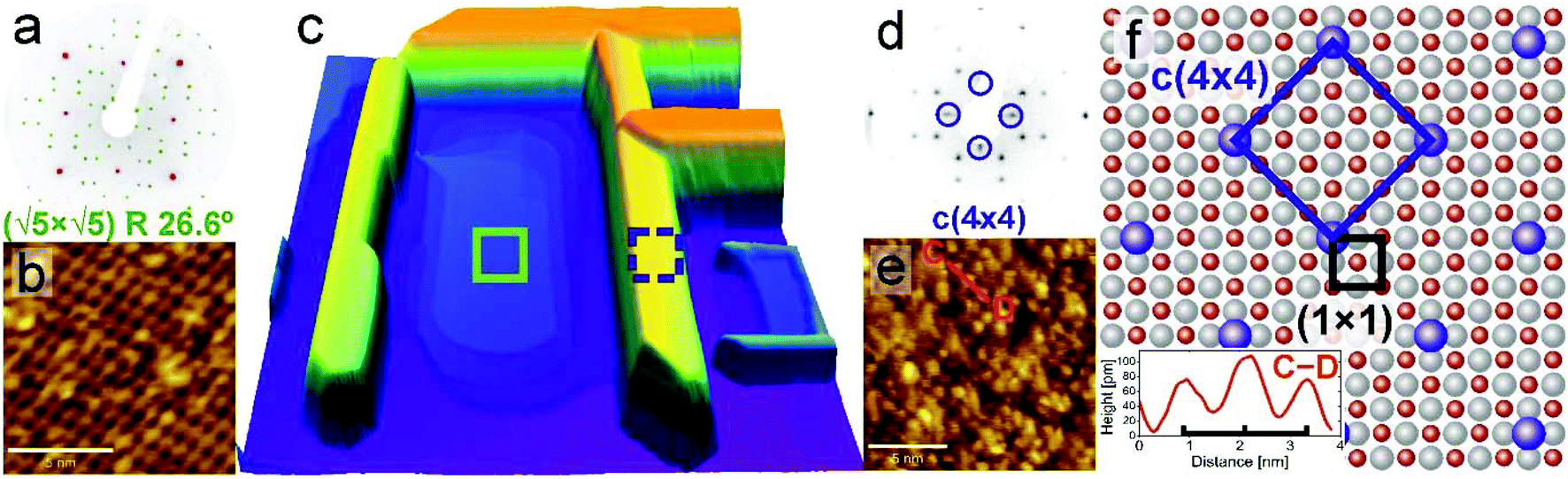 | ||
| Fig. 2 Surface structure of nanowires and the surface between them. (a) LEED pattern of a reduced SrTiO3 crystal (EBEAM = 100 eV). (1 × 1) and (√5 × √5)R26.6° reconstructions are marked in red and green respectively; (b) corresponding STM image of a (√5 × √5)R26.6° reconstruction; (c) 3D view of a TiO nanowire matrix formed on SrTiO3(100); (d) LEED pattern of the same reduced SrTiO3 crystal, with a new c(4 × 4) reconstruction marked in blue (EBEAM = 33 eV); (e) corresponding STM image of the c(4 × 4) reconstruction recorded at the top surface of the nanowire; and (f) model of the c(4 × 4) superstructure superimposed on a TiO (1 × 1) surface. | ||
3.3. Crystallography
Determining the actual surface structure is important; however the charge transfer efficiency and its mobility are greatly affected also by the interior structure and interface properties between nanowires and the substrate. According to the literature, there are four TiO phases: α, β, γ and the recently found ε-TiO.38,39 Here, TiO nanowires adopt a cubic rock salt γ-TiO structure as proved by STEM (Fig. 3, no filtering applied). A single nanowire, cut perpendicularly to its long axis, and parallel to the [001] direction of STO, is presented in Fig. 3(a). HAADF STEM imaging along the (001) zone axis reveals that nanowires are made of crystalline TiO with a lattice unit cell of 4.18 Å which is in excellent agreement with the literature value (PDF: #89-3660). Moreover, the STO substrate adopts a perovskite structure with easily distinguishable Sr and Ti + O columns and a lattice parameter of 3.9 Å. To compensate the strain induced by lattice misfit a complex zig-zag interface was formed (see also the inset in Fig. 3a) and additionally the TiO crystal structure was tilted by 4.6 degrees (also seen by EBSD analysis – see the ESI†). This tilt accounts for strain relaxation and together with the apparent zig-zag structure of the TiO/SrTiO3 interface is explained in section 3.5. High crystallographic order of both TiO and STO is additionally proven by nanodiffraction patterns (see the ESI†). Unlike previous observations,26 the presented TiO nanostructures and the SrTiO3 substrate seem to be virtually free of defects. The E–F line profile across the TiO/STO interface reveals a sharp transition, within one unit cell, from strontium titanate, with columns of Sr and Ti + O, to titanium monoxide with Ti + O atoms only (Fig. 3(c)). The atomic number Z-contrast in HAADF STEM imaging is clearly visible, since Sr (mass of 88 u) contributes to a much higher intensity than Ti and O (mass of 48 and 16 u, respectively).40 To gain deeper insight into the valence state at the interface, where for many oxide heterostructures exotic electronic states are localized,20,41 the EELS study, from the area marked in a dashed white box, was performed (Fig. 3(b)). Comparing the energy loss fine structure of the Ti L-edge with reference spectra enables tracking the actual evolution of the cation (here Ti) valence state at the TiO/SrTiO3 interface.42 In the presented case, the Ti4+ oxidation state corresponds to the titanium in octahedral coordination in SrTiO3, whereas Ti2+ are octahedrally coordinated atoms in the TiO rock-salt structure. Ti L-edge spectra from the nanowire region and the STO matrix are presented in Fig. 3(d), reflecting the changes in the near-edge structures of the Ti-L2,3 edges due to the increasing Ti valence and the effects of the crystal field. Two L3 and L2 peaks separated by 5 eV visible in the case of TiO can be attributed to the spin–orbit splitting of a Ti 2p core hole,15 whereas the SrTiO3 spectrum clearly shows further splitting of L2,3 peaks followed by a chemical shift, corresponding to the pure Ti4+ valence state. It can be explained based on the molecular orbital theory.43 Ti 2p core levels can be excited either to the 3eg or the 2t2g state, with the latter occupied in the case of TiO, resulting in two peaks instead of four for SrTiO3 (more detailed spectra and study are presented in the ESI†). From the line profile of the actual valence state (Fig. 3b) it is apparent that both Ti4+ and Ti2+ intensities change rapidly at the interface, by 60% within one unit cell. Even though the crystallographic structures of TiO and SrTiO3 have 6% lattice misfit, the interface is atomically sharp, probably due to the substantial content of Ti3+ contributing to interface stabilization. This sharp TiO/SrTiO3 interface may contribute to enhanced conductivity and magnetic properties, as postulated for polar/non-polar interfaces.44 The chemical composition of the wider area is determined using EDX mapping (Fig. 3(e)–(h)). Importantly, there is no Sr diffusion into the nanowire, meaning that the phase separation is definitive.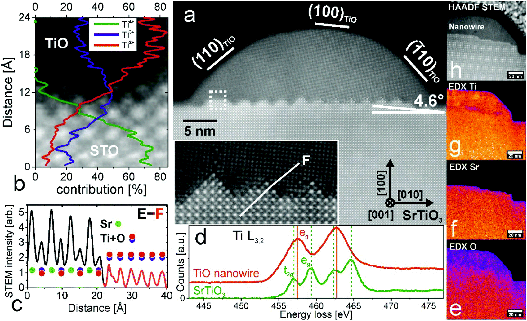 | ||
| Fig. 3 Crystallographic structure of a single TiO nanowire. (a) HAADF STEM image of a TiO nanowire grown on a SrTiO3(100) surface (for raw images see the ESI†). TiO and SrTiO3 crystallographic directions are shown. Inset: Magnified interface area showing the sharp zig-zag structure. (b) Ti valence state at the TiO/SrTiO3 interface (dashed box from (a)) measured by EELS. Ti4+, Ti3+ and Ti2+ concentrations are plotted. (c) Intensity profile across the STO (black) and TiO (red) interface (E–F line from (a) inset). (d) Ti L-edge spectra measured on the STO matrix and TiO nanowire by EELS. (e–h) EDX element mapping performed on a different TiO nanowire grown on SrTiO3; (e) EDX map of the O concentration; (f) EDX Sr concentration from the same area; (g) EDX Ti concentration; and (h) HAADF STEM image of a TiO nanowire. | ||
3.4. Conductivity
The resulting structure of the TiO nanowires could be employed as an array of nanoscale metallic electrodes e.g. for optimizing the performance of solar cells, organic devices and also for catalytic applications. To prove the excellent conductivity properties of nanowires, nanoscale current mapping was performed, in situ after reduction, using the LC-AFM method, allowing the measurement of the conductivity independently from the measurement of the topography. Local current mapping (Fig. 4(b)) indicates that the electric conductivity of the nanowires is at least 3 orders of magnitude higher than that of the STO surface between them. From the LC-AFM I/V curve (the inset to Fig. 4(b)), which shows ohmic behaviour, one can estimate the conductance of the whole system (tip + contact + TiO nanowire + interface + STO bulk) to be GLCAFM = 500 μS, which is two orders of magnitude higher than that in the case of reduced Nb-doped TiO2,45 a commonly used conducting substrate. Current maps prove that the high conductivity of the nanowires is not dependent on whether they are separated from each other (reduction temperatures around 1000 °C) or connected in the network (for higher temperatures of reduction). Moreover, conductivity properties remain virtually unchanged after oxidation, as we have demonstrated by dosing 100 Langmuir of pure O2in situ into the microscope chamber. The resulting current map of the oxidized surface is shown in Fig. 4(d). For comparison, we have proven recently that even a few Langmuir of oxygen are sufficient to switch off the conductive Sqrt5 surface of reduced SrTiO3.28 Apparently, even a higher dose does not affect the electronic properties of the TiO structures, which is crucial information for using TiO arrays in real systems, operating under ambient conditions.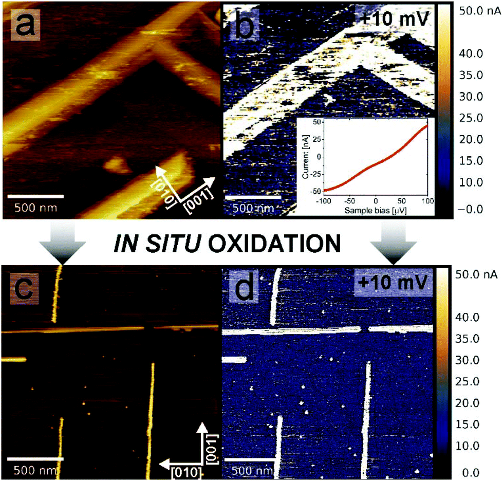 | ||
| Fig. 4 Conductivity of the TiO nanowire array. (a) LC-AFM topography of TiO nanowires grown on reduced SrTiO3; (b) corresponding current map collected with a +10 mV tip bias. Inset: I/V curve collected at one point on the nanowire's surface; (c), (d) topography and current of TiO nanowires on SrTiO3 after in situ oxidation. 100 Langmuir of pure O2 were dosed into the microscope chamber and the excellent conductivity properties of the nanowires remained. | ||
3.5. Growth mechanism
The intriguing issue is the origin of the high conductivity of nanowires placed on a nominally semiconducting/insulating substrate. In reality, even in the purest SrTiO3 crystals available on the market dislocations are present, arising from the growth limitations as well as from applied polishing and cutting procedures. When reduced, dislocations act as electrically conducting paths.21,46,47 In the present case, it is most likely that TiO nanowires are pinned to the dislocations in the STO crystal (see also the ESI†). Hence, the electric current flowing from the nanowires uses low resistance paths of reduced dislocations and the total conductance is very high. The dislocation cores of reduced crystals have up to 3 orders of magnitude less resistivity than the STO surface,47 which is in perfect agreement with our measurements of nanowire/surface conductivity. Since dislocations are easy to reduce but they are not so good in oxygen transport,48 crystal oxidation does not affect the conductance of the nanowires significantly, especially when the dislocation exits are additionally protected by a layer of TiO. This conclusion is further supported by the observation of structures formed at the edges of a crystal which was mechanically cut and thus ordered dislocations were introduced by the applied stress. There, a 1D linear structure of nanowires, which grew parallel to the cut edge, evolved (see the ESI†). It has already been proved that dislocations formed due to the plastic strain engineering have enhanced electronic properties with respect to the crystal matrix.49 In the present case it could open up the opportunity to create desired TiO nanowire patterns. Moreover, a possibility of creating dislocation bands via indentation, in both <001> and <011> crystallographic directions,50,51 allows for the precise designation of a nanowire growth site, with submicrometre precision.The creation of a new TiO phase out of a SrTiO3 single crystal requires a particular explanation. High annealing temperatures alone are not sufficient for the triggering of SrTiO3 decomposition since in many literature studies SrTiO3 proved to be stable even upon 1200 °C annealing.34 We address this issue and present a mechanism we call ELOP (extremely low oxygen partial pressure). Our recent study revealed that the use of getter materials such as Ti or TiO during reduction of perovskite crystals lowers significantly the oxygen partial pressure to values of 10−15 to 10−25 mbar, even if the base pressure of the vacuum system is much higher.52 This triggers the incongruent sublimation of strontium from the crystal. In the present case we used a SrTiO3/Si crystal sandwich, where the latter acted as a heater and as an oxygen getter simultaneously (see Fig. 5(a)). The use of an external getter proved to be a necessary condition for the formation of Ti-rich phases. When the STO crystal was annealed under exactly the same experimental conditions, but without silicon, no nanowires emerged. The influence of Si on macroscopic sublimation of SrTiO3 was checked by a separate experiment where a mass spectrometer was used to detect Sr coming from an annealed STO/Si admixture. The presence of silicon caused STO to decompose via incongruent sublimation (Fig. 5(e)) due to the enforced global oxygen deficiency. Importantly, no silicon was incorporated into the STO sample, as proven by EDX measurements. It is worth noticing that substantial Sr effusion started when the annealing temperature reached 950 °C, which is consistent with the observation of TiO nanowires starting to emerge at the same temperatures (Fig. 1).
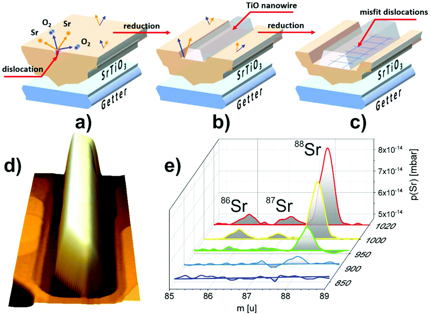 | ||
| Fig. 5 Macroscopic view of the growth of TiO nanowires on SrTiO3 at an extremely low oxygen partial pressure (ELOP). (a) Due to the lowered oxygen partial pressure, SrTiO3 decomposition starts preferentially at dislocations; (b) with prolonged reduction, due to the crystallographic shearing and surface diffusion, TiO nanowire network develops; (c) after a certain thickness is reached, strain relaxes and dislocations in the TiO are formed; (d) 3D view of the actual depression around a nanowire grown at 1100 °C (TM-AFM image); (e) strontium effusion from the SrTiO3/Si sandwich during reduction at different temperatures under extremely low oxygen partial pressure, detected using a mass spectrometer. | ||
To illustrate the first stages of the TiO nanowire growth we developed an empirical model shown in Fig. 6 (more detailed description in the ESI†). We assume that the formation of the nanowires can preferentially start on dislocation exits since it has been reported that during reduction their cores adopt a TiO nanophase.53 At first, during annealing, the Si getter triggers reduction and subsequent decomposition, which occurs over the whole surface, but is initiated first at the dislocation exits, due to the lowered enthalpy of formation of O vacancies (Fig. 5a).48 SrTiO3 decomposes locally and gaseous Sr and O2 species are released, leaving TiO6 octahedra with oxygen vacancies under the extremely low oxygen partial pressure established by the Si getter. Then, a Ti-enriched phase may form due to a crystallographic shearing mechanism, a typical process for the transformation of TiO2 into Magnéli phases (which additionally exhibit high electrical conductivity).2,54 Point defects (here oxygen vacancies) accumulate and form planar defects, e.g. Wadsley defects, which could then be annihilated via crystallographic shearing, resulting in the evolution of a new TiO phase.55 Due to the locally lowered oxygen partial pressure (higher oxygen vacancy concentration) induced by the presence of TiO, the SrTiO3 crystal decomposes further and the process continues, with more material being absorbed to the nanowire (Fig. 6 (3) and (4)). In addition to crystallographic shearing, diffusion of TiO on the surface is anticipated as a movement of a Ti–O pair, which was found to have a lower energy barrier in the case of in-channel and cross-channel diffusion in TiO2.56 This scenario is further proved by depressions around nanowires, as seen e.g. in Fig. 1a (inset, marked by red arrows) and in Fig. 5d showing a 3D view of a single nanowire. The closest vicinity of nanowires is always lowered, due to the finite diffusion length of Ti–O adspecies and the limited radius of crystallographic shearing. TiO nanowires grow, although the 6% misfit between TiO and STO lattices results eventually in relaxation in the form of dislocations formed in the TiO crystal, close to the interface (see Fig. 6 bottom row). When the TiO layer is thin enough, approx. below 10 atomic layers, the crystal is aligned according to the STO substrate (see the dashed box) although stress accumulates. Then, edge dislocations in the <001> directions are formed (see also Fig. 5c) and eventually a microscopic tilt of 4.6° appears. Formation of dislocations at the TiO/STO interface explains additionally the zig-zag shape of an interface. It is known that in oxides cation vacancies are formed preferentially in close proximity to the dislocations (e.g. in the case of MgSiO3![[thin space (1/6-em)]](https://www.rsc.org/images/entities/char_2009.gif) 57). Also in the case of the MgO–Mg system, dislocations proved to be easy paths for Mg sublimation.58 In our case, misfit dislocations can act as pipes for the Sr and O diffusion from the STO layer at the interface, enabling the transformation to rocksalt TiO and formation of the observed zig-zag intrusions.
57). Also in the case of the MgO–Mg system, dislocations proved to be easy paths for Mg sublimation.58 In our case, misfit dislocations can act as pipes for the Sr and O diffusion from the STO layer at the interface, enabling the transformation to rocksalt TiO and formation of the observed zig-zag intrusions.
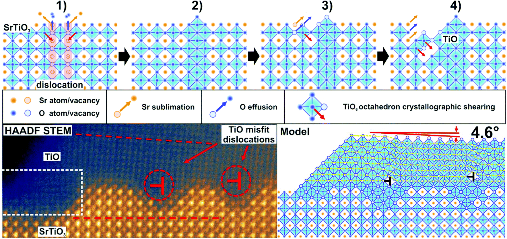 | ||
| Fig. 6 Schematic model of SrTiO3 decomposition and initial stages of TiO nanowire formation: (1) due to the heavy reducing conditions (lowered oxygen partial pressure and high temperature) Sr and O effuse from the surface and the process starts preferentially at dislocation exits, (2) due to the crystallographic shearing of TiO6 octahedra, a new TiO phase is formed, (3), (4) the process continues in the vicinity of a new phase and results in nanowire formation along <001> directions. Bottom: HAADF STEM image of a TiO nanowire formed on SrTiO3. Dislocations formed due to strain relaxation are marked. The ball-and-stick model on the right hand side depicts the actual TiO/STO interface from the HAADF STEM image. | ||
We expect that the same growth mechanism is applicable to other perovskites and analogous binary oxide structures can be created. In the study of Kolpak et al. some structures resembling nanowires, called their “precipitates”, are formed in the case of BaTiO3 UHV annealing.59 On the basis of presented research it is much likely that these structures are TiO nanowires. Hence, the ELOP mechanism of the incongruent sublimation can be employed for growth of various oxide nanostructures (depending on the actual equilibrium vapour pressures in the system).52 Moreover, we believe that unintentional lowering of the oxygen partial pressure by getter materials present in the close vicinity of the sample (e.g. sample holder, clamps) is the cause of the huge discrepancies of transition temperatures of surface reconstruction mentioned in section 3.2.
4. Conclusions
In conclusion, we have developed a way to form a crystalline TiO matrix on the surface of SrTiO3(100), an archetypal perovskite oxide. Our ELOP (extremely low oxygen partial pressure) method is based on crystal reduction under very low oxygen partial pressures, realized by use of an oxygen getter. With this, one can produce a large-scale array of titanium monoxide nanowires, with an excellent metallic conductivity, even after oxidation, on account of the connection with the dislocation network. We demonstrate that TiO and reduced SrTiO3 crystal structures are almost defect-free, with an atomically sharp zig-zag interface between them. To relate the observed electrical properties to the microstructure and chemistry on the nanoscale, using a combined TEM – EELS technique, we have succeeded in tracking the structural changes in the TiO/STO interface at the atomic scale. Due to the abrupt Ti valence state transition, exotic electronic states are expected. The actual formation of TiO nanowires is caused by the incongruent effusion of Sr, further decomposition of SrTiO3 and the crystallographic shearing of TiO6 octahedra. We propose a method of nanopatterning the crystal surface with TiO nanowires, taking advantage of their connection with the dislocation network. The use of plastic strain engineering and indentation allows for controlling the formed TiO nanowire network orientation and spacing. We finally believe that our ELOP method may be utilized in the broad class of oxide crystals and therefore improve efficiency of various catalytic and electronic devices. In addition to the intentional fabrication of suboxide structures on surfaces of transition metal oxides, our findings may also help understand huge discrepancies among literature studies on the thermal reduction process, as demonstrated for the case of SrTiO3(100) surface reconstruction evolution. Therefore, we suggest that materials for sample holders, heaters, and manipulators should be selected with utmost care, bearing in mind that in most cases they may affect the preparation procedure and, as a consequence, experimental results.Conflicts of interest
There are no conflicts to declare.Acknowledgements
We gratefully acknowledge P. Meuffels and R. Waser for fruitful discussions. We would like to additionally thank M. Castell for his valuable comments and support. Support by the Polish National Science Center (2017/24/T/ST5/00427 and 2015/19/B/ST5/01841) and the Deutsche Forschungsgemeinschaft (SFB 917 “Nanoswitches”) is acknowledged. We would like to express our gratitude to A. Budkowski and J. Rysz for providing access to AFM equipment.Notes and references
- V. Adamaki, F. Clemens, P. Ragulis, S. R. Pennock, J. Taylor and C. R. Bowen, J. Mater. Chem. A, 2014, 2, 8328–8333 RSC.
- A. F. Arif, R. Balgis, T. Ogi, F. Iskandar, A. Kinoshita, K. Nakamura and K. Okuyama, Sci. Rep., 2017, 7, 3646 CrossRef PubMed.
- M. T. Greiner and Z.-H. Lu, NPG Asia Mater., 2013, 5, e55 CrossRef CAS.
- X. Chen, L. Liu and F. Huang, Chem. Soc. Rev., 2015, 44, 1861–1885 RSC.
- D. Wang, C. Huang, J. He, X. Che, H. Zhang and F. Huang, ACS Omega, 2017, 2, 1036–1039 CrossRef CAS.
- C. Zhang, F. Hao, G. Gao, X. Liu, C. Ma, Y. Lin, Y. Yin and X. Li, NPJ Quantum Mater., 2017, 2, 2 CrossRef.
- J. Xu, D. Wang, H. Yao, K. Bu, J. Pan, J. He, F. Xu, Z. Hong, X. Chen and F. Huang, Adv. Mater., 2018, 30, 1706240 CrossRef PubMed.
- A. Guerrero, S. Chambon, L. Hirsch and G. Garcia-Belmonte, Adv. Funct. Mater., 2014, 24, 6234–6240 CrossRef CAS.
- Z. Li, J. Zhang, B. Guan, D. Wang, L.-M. Liu and X. W. D. Lou, Nat. Commun., 2016, 7, 13065 CrossRef CAS PubMed.
- J. Jiang, Y. Li, J. Liu, X. Huang, C. Yuan and X. W. D. Lou, Adv. Mater., 2012, 24, 5166–5180 CrossRef CAS.
- M. Paßens, M. Moors, R. Waser and S. Karthäuser, J. Phys. Chem. C, 2017, 121, 2815–2821 CrossRef.
- E. Verrelli, D. Tsoukalas, P. Normand, A. H. Kean and N. Boukos, Appl. Phys. Lett., 2013, 102, 022909 CrossRef.
- N. G. Semaltianos, S. Logothetidis, N. Frangis, I. Tsiaoussis, W. Perrie, G. Dearden and K. G. Watkins, Chem. Phys. Lett., 2010, 496, 113–116 CrossRef CAS.
- P. Simon, B. Pignon, B. Miao, S. Coste-Leconte, Y. Leconte, S. Marguet, P. Jegou, B. Bouchet-Fabre, C. Reynaud and N. Herlin-Boime, Chem. Mater., 2010, 22, 3704–3711 CrossRef CAS.
- C.-N. Huang, J.-S. Bow, Y. Zheng, S.-Y. Chen, N. Ho and P. Shen, Nanoscale Res. Lett., 2010, 5, 972 CrossRef CAS PubMed.
- B. M. Pabón, J. I. Beltrán, G. Sánchez-Santolino, I. Palacio, J. López-Sánchez, J. Rubio-Zuazo, J. M. Rojo, P. Ferrer, A. Mascaraque and M. C. Muñoz, et al. , Nat. Commun., 2015, 6, 6147 CrossRef PubMed.
- Y. Lin, J. Wen, L. Hu, J. A. McCarthy, S. Wang, K. R. Poeppelmeier and L. D. Marks, Micron, 2015, 68, 152–157 CrossRef CAS PubMed.
- F. Cardarelli, Materials handbook: a concise desktop reference, Springer Science & Business Media, 2008 Search PubMed.
- J.-F. Ge, Z.-L. Liu, C. Liu, C.-L. Gao, D. Qian, Q.-K. Xue, Y. Liu and J.-F. Jia, Nat. Mater., 2015, 14, 285 CrossRef CAS PubMed.
- N. Reyren, S. Thiel, A. D. Caviglia, L. F. Kourkoutis, G. Hammerl, C. Richter, C. W. Schneider, T. Kopp, A.-S. Rüetschi and D. Jaccard, et al. , Science, 2007, 317, 1196–1199 CrossRef CAS PubMed.
- K. Szot, W. Speier, G. Bihlmayer and R. Waser, Nat. Mater., 2006, 5(4), 312 CrossRef CAS PubMed.
- R. Waser and M. Aono, Nat. Mater., 2007, 6, 833 CrossRef CAS.
- B. Rahmati, W. Sigle, J. Fleig, M. Konuma, U. Eigenthaler, C. Koch, P. A. Van Aken, J. Maier and M. Rühle, J. Phys.: Conf. Ser., 2008, 94, 12013 CrossRef.
- K. Szot and W. Speier, Phys. Rev. B: Condens. Matter Mater. Phys., 1999, 60, 5909 CrossRef CAS.
- D. T. Newell, A. Harrison, F. Silly and M. R. Castell, Phys. Rev. B, 2007, 75(20), 205429 CrossRef.
- S. B. Lee, F. Phillipp, W. Sigle and M. Rule, Ultramicroscopy, 2005, 104, 30–38 CrossRef CAS PubMed.
- M. S. J. Marshall, A. E. Becerra-Toledo, L. D. Marks and M. R. Castell, Phys. Rev. Lett., 2011, 107(8), 086102 CrossRef PubMed.
- D. Wrana, C. Rodenbücher, W. Bełza, K. Szot and F. Krok, Appl. Surf. Sci., 2018, 432, 46–52 CrossRef CAS.
- I. Arnay, J. Rubio-Zuazo and G. R. Castro, Appl. Surf. Sci., 2018, 427, 561–565 CrossRef CAS.
- A. Biswas, C.-H. Yang, R. Ramesh and Y. H. Jeong, Prog. Surf. Sci., 2017, 92, 117–141 CrossRef CAS.
- J. Hanzig, M. Zschornak, E. Mehner, F. Hanzig, W. Münchgesang, T. Leisegang, H. Stöcker and D. C. Meyer, J. Phys.: Condens. Matter, 2016, 28, 225001 CrossRef.
- K. Eom, E. Choi, M. Choi, S. Han, H. Zhou and J. Lee, J. Phys. Chem. Lett., 2017, 8, 3500–3505 CrossRef CAS.
- M. S. M. González, M. H. Aguirre, E. Morán, M. Á. Alario-Franco, V. Perez-Dieste, J. Avila and M. C. Asensio, Solid State Sci., 2000, 2, 519–524 CrossRef.
- T. Kubo and H. Nozoye, Phys. Rev. Lett., 2001, 86, 1801 CrossRef CAS PubMed.
- M. R. Castell, Surf. Sci., 2002, 516, 33–42 CrossRef CAS.
- J. M. P. Martirez, E. H. Morales, W. A. Saidi, D. A. Bonnell and A. M. Rappe, Phys. Rev. Lett., 2012, 109, 256802 CrossRef.
- E. H. Morales, J. M. P. Martirez, W. A. Saidi, A. M. Rappe and D. A. Bonnell, ACS Nano, 2014, 8, 4465–4473 CrossRef CAS PubMed.
- J. L. Murray and H. A. Wriedt, J. Phase Equilib., 1987, 8, 148–165 CrossRef CAS.
- S. Amano, D. Bogdanovski, H. Yamane, M. Terauchi and R. Dronskowski, Angew. Chem., Int. Ed., 2016, 55, 1652–1657 CrossRef CAS PubMed.
- W. Xu, P. C. Bowes, E. D. Grimley, D. L. Irving and J. M. LeBeau, Appl. Phys. Lett., 2016, 109, 201601 CrossRef.
- Y. Z. Chen, F. Trier, T. Wijnands, R. J. Green, N. Gauquelin, R. Egoavil, D. V. Christensen, G. Koster, M. Huijben and N. Bovet, et al. , Nat. Mater., 2015, 14, 801 CrossRef CAS.
- L. Fitting, S. Thiel, A. Schmehl, J. Mannhart and D. A. Muller, Ultramicroscopy, 2006, 106, 1053–1061 CrossRef CAS.
- Y. Zhang, C. Guerra-Nuñez, I. Utke, J. Michler, P. Agrawal, M. D. Rossell and R. Erni, Chem. Mater., 2017, 29, 2232–2238 CrossRef CAS.
- L. Yu and A. Zunger, Nat. Commun., 2014, 5, 5118 CrossRef CAS.
- D. Wrana, C. Rodenbücher, M. Krawiec, B. R. Jany, J. Rysz, M. Ermrich, K. Szot and F. Krok, Phys. Chem. Chem. Phys., 2017, 19(45), 30339–30350 RSC.
- R. Wang, Y. Zhu and S. M. Shapiro, Phys. Rev. Lett., 1998, 80, 2370 CrossRef CAS.
- R. Waser, R. Dittmann, G. Staikov and K. Szot, Adv. Mater., 2009, 21, 2632–2663 CrossRef CAS.
- D. Marrocchelli, L. Sun and B. Yildiz, J. Am. Chem. Soc., 2015, 137(14), 4735–4748 CrossRef CAS.
- K. K. Adepalli, J. Yang, J. Maier, H. L. Tuller and B. Yildiz, Adv. Funct. Mater., 2017, 27(22), 1700243 CrossRef.
- F. Javaid, A. Stukowski and K. Durst, J. Am. Ceram. Soc., 2017, 100, 1134–1145 CrossRef CAS.
- F. Javaid, E. Bruder and K. Durst, Acta Mater., 2017, 139, 1–10 CrossRef CAS.
- C. Rodenbücher, P. Meuffels, W. Speier, M. Ermrich, D. Wrana, F. Krok and K. Szot, Phys. Status Solidi RRL, 2017, 11(9), 1700222 CrossRef.
- H. Du, C.-L. Jia, L. Houben, V. Metlenko, R. A. De Souza, R. Waser and J. Mayer, Acta Mater., 2015, 89, 344–351 CrossRef CAS.
- M. Fujimoto and M. Watanabe, J. Mater. Sci., 1985, 20, 3683–3690 CrossRef CAS.
- C. R. A. Catlow, Nonstoichiom. Oxides, 1981, 61–98 CAS.
- M. Kolmer, A. A. Zebari, M. Goryl, F. B. de Mongeot, F. Zasada, W. Piskorz, P. Pietrzyk, Z. Sojka, F. Krok and M. Szymonski, Phys. Rev. B: Condens. Matter Mater. Phys., 2013, 88, 195427 CrossRef.
- P. Hirel, P. Carrez, E. Clouet and P. Cordier, Acta Mater., 2016, 106, 313–321 CrossRef CAS.
- Q. Yu, M.-M. Mao, Q.-J. Li, X.-Q. Fu, H. Tian, J.-X. Li, S. X. Mao and Z. Zhang, Nano Lett., 2016, 16, 1156–1160 CrossRef CAS.
- A. M. Kolpak, D. Li, R. Shao, A. M. Rappe and D. A. Bonnell, Phys. Rev. Lett., 2008, 101, 36102 CrossRef.
Footnote |
| † Electronic supplementary information (ESI) available. See DOI: 10.1039/c8nr04545c |
| This journal is © The Royal Society of Chemistry 2019 |