
Mechanochemical preparation of piezoelectric nanomaterials: BN, MoS2 and WS2 2D materials and their glycine-cocrystals†
Viviana Jehová
González
 a,
Antonio M.
Rodríguez
*a,
Ismael
Payo
b and
Ester
Vázquez
*ac
a,
Antonio M.
Rodríguez
*a,
Ismael
Payo
b and
Ester
Vázquez
*ac
aInstituto Regional de Investigación Científica Aplicada (IRICA), UCLM, 13071 Ciudad Real, Spain. E-mail: antoniom.rodriguez@uclm.es
bEscuela de Ingeniería Industrial y Aeroespacial de Toledo, UCLM, Avenida Carlos III s/n, Real Fábrica de Armas, 45071, Toledo, Spain
cFacultad de Ciencias y Tecnologías Químicas, UCLM, Avda. Camilo José Cela S/N, 13071, Ciudad Real, Spain
First published on 7th October 2019
Abstract
Different 2D-layered materials of transition metal dichalcogenides (TMDCs) such as boron nitride (BN) or molybdenum disulphide (MoS2) have been theorised to have piezoelectric behaviour. Still, the procedures to obtain these nanomaterials, with the right quality and quantity to observe the piezoelectric performance, are enormously expensive, halting their possible applications. Here, we show the mechanochemical exfoliation of 2D nanomaterials (FLG, BN, MoS2 and WS2) with glycine. We have also successfully synthesised the cocrystals for these nanomaterials, which makes it possible to enhance their piezoelectric responses.
New concepts2D nanomaterials have grown to include isolators (boron nitride, BN) and semiconductors (molybdenum and tungsten disulphide, MoS2 and WS2). Together with other different properties, the practical piezoelectricity of single-atomic layers of BN, MoS2 and WS2 has been underexplored in the last few years, especially regarding wide spread exploration to integrate these materials on ‘bio-friendly’ force sensors or solving problems with energy harvesting related applications. We believe that these materials could bridge the gap with other piezoelectric materials under mechanical stress situations out of their optimal frequencies. In this context, an efficient method for the exfoliation of these transition metal dichalcogenides (TMDCs) and the formation of their cocrystals is presented. Nanomaterial cocrystals are a novel concept within the Materials Sciences community, and we have obtained a cocrystal with enhanced piezoelectric properties from their starting materials. These could have an essential role in biological sensors or be imbedded in paints or inks to cover mobile devices, tablets, keyboards, or other large surfaces. In this case, the exfoliating agent is a biomolecule, glycine, which could also solve significant problems with biological integration in piezoelectric sensors or actuators. We have also experimentally proved the piezoelectric response of these materials with a simple setup. |
Piezoelectric materials have a unique property that converts mechanical energy into electrical energy or vice versa.1 Barium titanate was the first piezoelectric ceramic ever discovered, but the ceramic lead zirconate titanate, also known as PZT, is the most commonly used material for piezoelectric harvesting.2 Nevertheless, the extremely fragile nature of PZT ceramic and the incorporation of lead create issues such as the reliability, durability, and safety of this material for long-term sustainable operation.
2D materials and the possibility to modulate their composition in a well-controlled manner offer a platform that allows the creation of different heterostructures for a large variety of applications. Starting with graphene, 2D nanomaterials have grown to include insulators (boron nitride, BN), semiconductors (molybdenum disulphide, MoS2) and metals (Niobium diselenide, NbSe2).3 Together with other different properties, the theoretical piezoelectricity of single-atomic layers of boron nitride (BN), molybdenum disulfide (MoS2) and tungsten disulfide (WS2) as a function of strain-induced lattice distortion and ionic charge polarisation has been studied.4,5 The future prospects of these nanomaterials have been covered in the literature.6 Experimentally, some applications of this nanomaterial behaviour have been explored in energy conversion,7 voltage generators,8 pressure sensors,9 nonlinear energy harvesters,10 and transducers.11 The methodologies currently used in the production of these nanomaterials for nano-electromechanical applications are mainly based on chemical vapour deposition (CVD). This technique presents some problems, such as the high cost and necessity to deposit on other materials, which can lead to compatibility issues. Additionally, in real-world applications, the environmental impact of producing any device should always be considered beforehand, and one fundamental problem is to scale up experiments in a safe, secure and efficient way. In that sense, mechanochemical exfoliation of 2D materials has gained increasing importance in the last few years.12–15 These protocols have many advantages over their liquid-phase counterparts, including processes with shorter reaction times, higher product yields and the elimination of (harmful) organic solvents, which make this approach more sustainable and cheaper. Some examples have seen molecules such as sucrose, urea and boric acid used as exfoliating agents.16–18 Nowadays, there are no examples of the application of TMDC nanomaterials in piezoelectric paint, coatings or adhesive matrices which could be easily applied to heterogeneous surfaces paving the way for applications such as sensors,19 or power sensors20 and nanosystems for energy harvesting applications.21,22
On the other hand, in the past 60 years, piezoelectricity has been confirmed in a variety of biological materials; for example, fibrous protein collagen,23 elastin,24 bone25 (calcified collagen), wood,26 and some viruses27 exhibit relatively modest piezoelectricity (0.1–10 pm V−1). Classical piezoelectric principles have also been applied to similar uniaxially orientated, bioactive polymers, such as poly(L-lactic acid) (PLLA), poly (γ-benzyl glutamate) (PBG), and cellulose.28 The only non-chiral amino acid, glycine, has been known to crystallize in three distinct polymorphs (α)-alpha,29 (β)-beta,30 and (γ)-gamma glycine31 under ambient conditions.32 The crystallization of α-glycine occurs in the centrosymmetric space group P21/c, which precludes piezoelectricity. On the other hand, β-glycine and γ-glycine belong to the non-centrosymmetric space groups P21 and P32, respectively, and so should exhibit a non-zero piezoelectric response. A modest ‘effective' shear and longitudinal piezoelectricity have been measured for β-glycine (6 pm V−1) and γ-glycine (10 pm V−1), respectively,33,34 using piezo response force microscopy (PFM).35
In our previous work, we have investigated the exfoliation procedures of graphite to graphene using ball milling techniques in the presence of carbohydrates.36 We could also prepare glucose–graphene cocrystals as biocompatible systems. In this work, we have explored the exfoliation of 2D nanomaterials using the amino acid glycine. In a second step, the formation of glycine-nanomaterial cocrystals has proven to enhance the piezoelectric properties of the exfoliated material. The relative ease of production of these materials through our mechano-chemical process would significantly impact their presence in future applications. In this study, we proposed a mechanochemical exfoliation of TMDCs and other 2D nanomaterials, such as BN and FLG, and the study of their intrinsic piezoelectricity. Furthermore, our objective aims to integrate the nanomaterials in supramolecular organic matrices, such as cocrystals that would enhance their piezoelectricity.
Based on our previous experience on mechanochemical exfoliation of graphite, we performed the ball-milling treatment in solvent-free conditions adding glycine as the exfoliant agent and graphite in a 250 mL stainless-steel grinding bowl with 15 stainless steel balls (2 cm diameter each) at 250 rpm. The detailed experimental procedure is described in the ESI.† Since no precipitate was observed in the resulting dispersions, they were entirely lyophilised after the dialysis. The best experimental conditions for obtaining graphene materials of two different sizes and the yields are represented in Table S1 (ESI†).
Fig. S1 (ESI†) displays the Raman spectra of FLG1 and FLG2, showing the different characteristic bands present in carbon nanomaterials (D, G and 2D).37,38 It is possible to observe that the ID/IG value between the different peaks in sample FLG1 is 0.39 in comparison with FLG2, 1.63. This data correlates with the minor size of FLG2 flakes (Table S1 and Fig. S2, ESI†) which shows a direct relation with the time of mechanochemical treatment. Thermogravimetrical analysis (TGA) of these materials is collected in Fig. S3 (ESI†). Our analysis showed a minor presence of nitrogen attached on the graphene layer with a minor presence of oxygen and organic groups on the surface of graphene (2% loss in TGA). We can draw similar conclusions regarding the TGA loss for both FLG1 and FLG2 nanomaterials as in our previous works.36
Based on these good results, the high-quality exfoliation with very high yields and the smooth, sustainable and low-cost procedure, we decided to extrapolate these experimental procedures to the exfoliation of other 2D-layered materials such as BN, MoS2 and WS2. The experimental conditions for the 2D nanomaterial exfoliation are collected in Table S1 (ESI†). Powder X-ray Diffraction (PXRD) of the exfoliated materials and the raw nanomaterials are all shown in Fig. S4 (ESI†). In all cases, the X-ray diffraction patterns show a clear decrease in the number of counts on the 002-diffraction pattern. For the example of BN, which has the lowest reduction, it is known that the intensity ratio of (BNraw)002/(BNexfo)002 of approximately 2.5 already indicates thin BN layers and much weaker stacking at the c-direction in the exfoliated sample.39,40
Fig. S5 (ESI†) shows the Raman spectra of the MoS2 system, although both WS2 and MoS2 have similar patterns. Both nanomaterials possess two primary Raman modes, one in-plane mode of Mo or W–S bond (E2g) another out-of-plane mode (A1g) at around 380 and 405 cm−1 (MoS2), and 350 and 415 cm−1 (WS2).41 It is possible to observe a blueshift and a redshift in A1g mode for MoS2 and WS2, respectively, which corresponds to a decrease in the number of layers (Table S2, ESI†). According to the diagrams of Terrones et al. for WS2 nanomaterials,42 we have a relation of IE2g/IA1g of 0.69, which corresponds to a value of 3 layers for our WS2 exfoliated nanomaterial. With respect to MoS2,43 according to the distance between the bands E12g and A11g, the average number of layers is around 3. Finally, BN exhibits a characteristic Raman peak for the E2g phonon mode (B–N vibration mode) around 1365 cm−1‚44 which is analogous to the E2g mode (G band) in graphene. Moreover, a slight blue shift in the E2g peak is consistent with the exfoliation of BN.45 TEM images (Fig. 1) show the exfoliated dichalcogenide with the corresponding distribution of lateral size in Table S1 (ESI†). As shown in Fig. S6 (ESI†), the TGA curves of exfoliated nanomaterials show a reduced weight loss compared with those of the pristine 2D nanomaterial because of the small residue of the exfoliant agent. Also, a wide scan XPS spectrum has been included in the ESI† to rule out the presence of other impurities (Fig. S7 and Table S3, ESI†). The atomic content (in %) corresponding to C, N, H and O also correlates with the small quantities of exfoliant agent. Raw and exfoliated materials are not expected to contain C and O. However around 10% of the undesired C and O content probably arises from CO and CO2 species in air, adsorbed on the substrates.46 Nevertheless, further analysis of the samples has shown that the sample BNexfo has a residue amount of glycine around 20%, which also corresponds to our TGA analysis (in Fig. S6, ESI†).
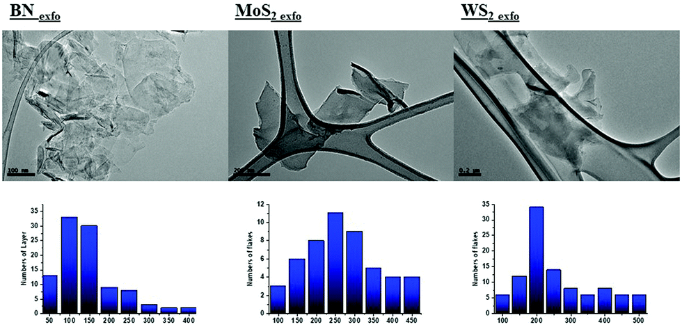 | ||
| Fig. 1 TEM images and distributions of sizes for the different 2D nanomaterial samples. | ||
These results are similar to those observed in the literature.47
After demonstrating the exfoliation of 2D nanomaterials, we studied the formation of glycine cocrystals following a similar procedure of lyophilization (ESI†). The PXRD study for all the different materials indicated that the cocrystal structures differed wildly from the original nanomaterials or the initial glycine crystal structure (Fig. 2 for the BN). The appearance of some new peaks (between 20 and 65°) corresponds to the different reflections of α, β, and γ-glycine phases in the cocrystal sample and other new peaks are observed in that same region, which do not correspond to any raw material. Those new peaks can be attributed to new cocrystal structures. Similar results are observed for other nanomaterials (Fig. S8, ESI†). It seems that the presence of the nanomaterial in dispersion together with the crystallization of water while freezing, “pressed out” glycine forcing the appearance of different polymorphisms. This is a process known from the literature,48,49 and it correlates well with our understanding of the important interactions between water molecules, exfoliating agents and 2D materials.50 The TGA for the 2D nanomaterial cocrystals shows a similar loss to glycine, which might be due to the high content of such a molecule. The 3 wt% difference between glycine and the cocrystal measurement, corresponds to the presence of the nanomaterial in the cocrystal structure. The structure of glycine cocrystals has been investigated, showing the presence of γ and β-glycine. Commercial glycine was similarly ground as the benchmark sample, resulting in β-glycine majority and with similar piezoelectric response to initial glycine. A comparison of the powder X-ray diffraction results of these samples can be found in Fig. S9 (ESI†). Further study of the Raman spectra of 2D nanomaterial glycine cocrystals pointed to modifications on the vibrational mode frequencies of the intermolecular and intramolecular bonds in the samples. This could correspond to the appearance of new crystal forms and it also gives information on the quality of the exfoliated nanomaterials (Fig. S10, ESI†).
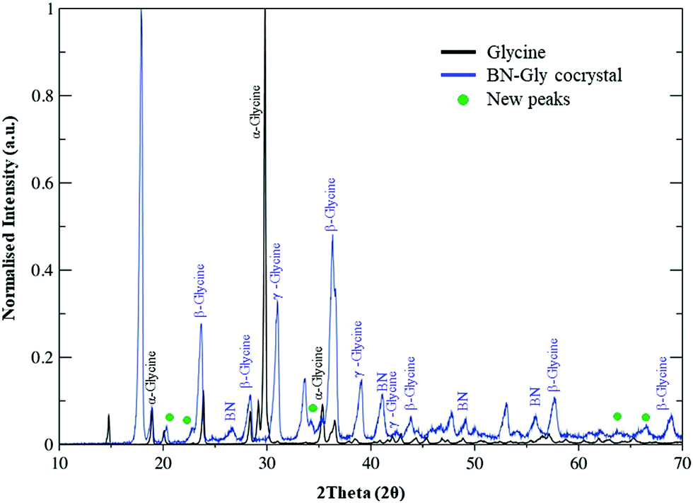 | ||
| Fig. 2 Powder X-ray diffraction results for glycine and BN–glycine cocrystals. | ||
Finally, preliminary studies on the piezoelectricity of the exfoliated nanomaterials and the glycine cocrystal forms were performed. Fig. 3 shows the experimental setup used for dynamic testing of the piezoelectricity. Results were amplified with an electronic circuit as shown in Fig. S11 (ESI†). The nanomaterials were placed in a simple system, sandwiched between electrodes of area 1 cm2, under a force of 10 N. This experimental setup mimics those described in the literature for the experimental corroboration of the piezoelectricity of different materials in powder form.51
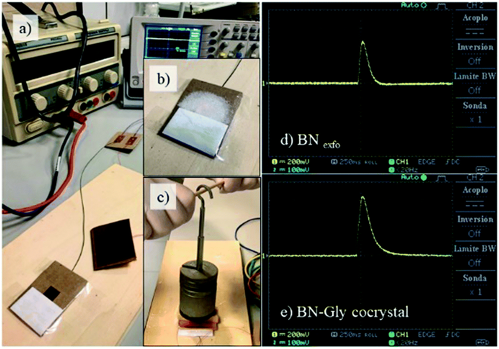 | ||
| Fig. 3 (a) Experimental set up for piezoelectricity measurements. (b) Layer of cocrystals on a square copper electrode (10 mm × 10 mm), insulated with paper. (c) Manual compression of a 2D nanomaterial crystal layer. (d) Piezoelectric response of exfoliated BN nanomaterials. (e) Measured piezoelectric response with exfoliated BN cocrystals. | ||
The piezoelectricity behaviour is better in the cocrystal form than in the exfoliated material or with unpolarized PZT powders (Table 1, Fig. S12 and S13, ESI†) or other organic piezoelectric materials. We obtained similar results for all nanomaterials in their cocrystal forms, with a maximum open-circuit voltage of 150 mV N−1 for the MoS2–Glycocrystal. Similar results could be observed with the MoS2 and WS2 at the same range of induced strain (Table 1). For comparison purposes, we also mixed thoroughly the samples of the exfoliated samples and the glycine cocrystal separately (Table 1 samples: 2D nanomaterial + Glymix), but it showed less piezoelectric response.
| Sample | Piezoelectric response (mV N−1) |
|---|---|
| a These nanomaterials can’t be properly measured because their relatively high conductivity short-circuited the electronic circuit. b Given the semiconductor behaviour of MoS2, the materials could be working as a super-capacitor in the measurement. The corresponding figures can be found in the ESI. | |
| PZT | 16 |
| Polyvinylidene fluoride (PVDF) | 48 |
| Glycine (Gly) | 12 |
| Glygrinded | 15 |
| Glylyophilized | 36 |
| BNraw | 8 |
| BNexfo | 48 |
| BN–Gly cocrystal | 64 |
| BNexfo + Gly-mix | 37 |
| WS2raw | —a |
| WS2exfo | —b |
| WS2–Gly cocrystal | 88 |
| WS2exfo + Gly-mix | 60 |
| Graphite | —a |
| FLGexfo | —a |
| FLG–Gly cocrystal | 95 |
| FLGexfo + Gly-mix | 60 |
| MoS2raw | —b |
| MoS2exfo | —b |
| MoS2–Gly cocrystal | 150 |
| MoS2exfo + Gly-mix | 78 |
Also, both BN and WS2 cocrystals showed outstanding responsiveness under lower ranges of forces (around 1 N) and produced good recovery cycles and maintained in time (Fig. S14, ESI†). The remarkable piezoelectric character of these nanomaterials has all been measured without polarisation, while the standard procedure uses polarized materials for this sort of measurement.
Conclusions
We describe an easy and scalable method to enhance the piezoelectric responses of 2D nanomaterials. The process includes the preparation of glycine- 2D cocrystals in which the proportion of different polymorphisms of glycine is readily changed. These powder samples, with different 2D materials, can be used in the development of matrices with piezoelectric character. These materials could be imbedded in paints or inks to cover large surfaces, either in mobile devices, tablets, or keyboards, with improved piezoelectric properties. Future uses in sensors, power sensors or harvesting energy applications can be predicted.Conflicts of interest
There are no conflicts to declare.Acknowledgements
Financial support from the EU Graphene-based disruptive technologies, Graphene Flagship core 2 (785219) and the Spanish Ministerio de Economía y Competitividad (Project CTQ2017-88158-R) are gratefully acknowledged. Raman spectra were collected using a Spectrometer confocal Renishaw InVia Reflex (FEDER-JCCM funding, UNCM13-1E-1663), included in the facilities of the Instituto Regional de Investigación Científica Aplicada (IRICA), which is also acknowledged for technical support.Notes and references
- K. Uchino, Advanced Piezoelectric Materials, 2017, pp. 1–92, DOI:10.1016/b978-0-08-102135-4.00001-1.
- D. Damjanovic, Rep. Prog. Phys., 1998, 61, 1267–1324 CrossRef CAS.
- A. K. Geim and I. V. Grigorieva, Nature, 2013, 499, 419–425 CrossRef CAS.
- K. A. N. Duerloo, M. T. Ong and E. J. Reed, J. Phys. Chem. Lett., 2012, 3, 2871–2876 CrossRef CAS.
- A. A. M. Noor, H. J. Kim and Y. H. Shin, Phys. Chem. Chem. Phys., 2014, 16, 6575–6582 RSC.
- M. Samadi, N. Sarikhani, M. Zirak, H. Zhang, H.-L. Zhang and A. Z. Moshfegh, Nanoscale Horiz., 2018, 3, 90–204 RSC.
- W. Wu, L. Wang, Y. Li, F. Zhang, L. Lin, S. Niu, D. Chenet, X. Zhang, Y. Hao, T. F. Heinz, J. Hone and Z. L. Wang, Nature, 2014, 514, 470–474 CrossRef CAS.
- S. Yu, K. Eshun, H. Zhu and Q. Li, Sci. Rep., 2015, 5, 12854 CrossRef CAS.
- S. Wagner, C. Yim, N. McEvoy, S. Kataria, V. Yokaribas, A. Kuc, S. Pindl, C. P. Fritzen, T. Heine, G. S. Duesberg and M. C. Lemme, Nano Lett., 2018, 18, 3738–3745 CrossRef CAS.
- M. Lopez-Suarez, M. Pruneda, G. Abadal and R. Rurali, Nanotechnology, 2014, 25, 175401 CrossRef.
- F. Zhao, Y. Yao, X. Li, L. Lan, C. Jiang and J. Ping, Anal. Chem., 2018, 90, 11658–11664 CrossRef CAS.
- V. León, A. M. Rodríguez, P. Prieto, M. Prato and E. Vazquez, ACS Nano, 2014, 8, 563–571 CrossRef.
- V. Leon, J. M. Gonzalez-Dominguez, J. L. Fierro, M. Prato and E. Vazquez, Nanoscale, 2016, 8, 14548–14555 RSC.
- M. Buzaglo, E. Ruse, I. Levy, R. Nadiv, G. Reuveni, M. Shtein and O. Regev, Chem. Mater., 2017, 29, 9998–10006 CrossRef CAS.
- J. M. Gonzalez-Dominguez, V. Leon, M. I. Lucio, M. Prato and E. Vazquez, Nat. Protoc., 2018, 13, 495–506 CrossRef CAS.
- W. Lei, V. N. Mochalin, D. Liu, S. Qin, Y. Gogotsi and Y. Chen, Nat. Commun., 2015, 6, 8849 CrossRef CAS.
- S. Chen, R. Xu, J. Liu, X. Zou, L. Qiu, F. Kang, B. Liu and H. M. Cheng, Adv. Mater., 2019, 31, e1804810 CrossRef.
- C. Cao, Y. Xue, Z. Liu, Z. Zhou, J. Ji, Q. Song, Q. Hu, Y. Fang and C. Tang, 2D Mater., 2019, 6, 035014 CrossRef.
- J. R. White, B. de Poumeyrol, J. M. Hale and R. Stephenson, J. Mater. Sci., 2004, 39, 3105–3114 CrossRef CAS.
- M. J. Ramsay and W. W. Clark, Smart Structures and Materials 2001: Industrial and Commercial Applications of Smart Structures Technologies, 2001, vol. 4332, pp. 429–438 Search PubMed.
- Z. L. Wang, Nano Res., 2008, 1, 1–8 CrossRef CAS.
- Z. L. Wang, Nano Today, 2010, 5, 512–514 CrossRef.
- E. Fukada and I. Yasuda, Jpn. J. Appl. Phys., 1964, 3, 117–121 CrossRef CAS.
- Y. Liu, H. L. Cai, M. Zelisko, Y. Wang, J. Sun, F. Yan, F. Ma, P. Wang, Q. N. Chen, H. Zheng, X. Meng, P. Sharma, Y. Zhang and J. Li, Proc. Natl. Acad. Sci. U. S. A., 2014, 111, E2780–2786 CrossRef CAS.
- E. Fukada and I. Yasuda, J. Phys. Soc. Jpn., 1957, 12, 1158–1162 CrossRef.
- E. Fukada, J. Phys. Soc. Jpn., 1955, 10, 149–154 CrossRef.
- B. Y. Lee, J. Zhang, C. Zueger, W. J. Chung, S. Y. Yoo, E. Wang, J. Meyer, R. Ramesh and S. W. Lee, Nat. Nanotechnol., 2012, 7, 351–356 CrossRef CAS.
- E. Fukada, IEEE Trans. Electr. Insul., 1992, 27, 813–819 CrossRef CAS.
- G. Albrecht and R. B. Corey, J. Am. Chem. Soc., 1939, 61, 1087–1103 CrossRef CAS.
- Y. Iitaka, Nature, 1959, 183, 390–391 CrossRef CAS.
- Y. Iitaka, Acta Crystallogr., 1958, 11, 225–226 CrossRef CAS.
- A. Dawson, D. R. Allan, S. A. Belmonte, S. J. Clark, W. I. F. David, P. A. McGregor, S. Parsons, C. R. Pulham and L. Sawyer, Cryst. Growth Des., 2005, 5, 1415–1427 CrossRef CAS.
- R. Ashok Kumar, R. Ezhil Vizhi, N. Vijayan and D. Rajan Babu, Phys. B, 2011, 406, 2594–2600 CrossRef CAS.
- A. Heredia, V. Meunier, I. K. Bdikin, J. Gracio, N. Balke, S. Jesse, A. Tselev, P. K. Agarwal, B. G. Sumpter, S. V. Kalinin and A. L. Kholkin, Adv. Funct. Mater., 2012, 22, 2996–3003 CrossRef CAS.
- N. Balke, I. Bdikin, S. V. Kalinin and A. L. Kholkin, J. Am. Ceram. Soc., 2009, 92, 1629–1647 CrossRef CAS.
- V. J. González, A. M. Rodríguez, V. León, J. Frontiñán-Rubio, J. L. G. Fierro, M. Durán-Prado, A. B. Muñoz-García, M. Pavone and E. Vázquez, Green Chem., 2018, 20, 3581–3592 RSC.
- A. C. Ferrari, Solid State Commun., 2007, 143, 47–57 CrossRef CAS.
- A. C. Ferrari and D. M. Basko, Nat. Nanotechnol., 2013, 8, 235–246 CrossRef CAS.
- D. Fan, J. Feng, J. Liu, T. Gao, Z. Ye, M. Chen and X. Lv, Ceram. Int., 2016, 42, 7155–7163 CrossRef CAS.
- D. Lee, B. Lee, K. H. Park, H. J. Ryu, S. Jeon and S. H. Hong, Nano Lett., 2015, 15, 1238–1244 CrossRef CAS.
- G. Liu and N. Komatsu, ChemNanoMat, 2016, 2, 500–503 CrossRef CAS.
- A. Berkdemir, H. R. Gutiérrez, A. R. Botello-Méndez, N. Perea-López, A. L. Elías, C.-I. Chia, B. Wang, V. H. Crespi, F. López-Urías, J.-C. Charlier, H. Terrones and M. Terrones, Sci. Rep., 2013, 3, 1755 CrossRef.
- R. Shahzad, T. Kim and S.-W. Kang, Thin Solid Films, 2017, 641, 79–86 CrossRef CAS.
- L. Cao, S. Emami and K. Lafdi, Mater. Express, 2014, 4, 165–171 CrossRef CAS.
- R. B. Baig and R. S. Varma, Chem. Soc. Rev., 2012, 41, 1559–1584 RSC.
- E. Er, H.-L. Hou, A. Criado, J. Langer, M. Möller, N. Erk, L. M. Liz-Marzán and M. Prato, Chem. Mater., 2019, 31, 5725–5734 CrossRef CAS.
- X. Wang and P. Wu, ACS Appl. Mater. Interfaces, 2018, 10, 2504–2514 CrossRef CAS.
- N. V. Surovtsev, S. V. Adichtchev, V. K. Malinovsky, A. G. Ogienko, V. A. Drebushchak, A. Y. Manakov, A. I. Ancharov, A. S. Yunoshev and E. V. Boldyreva, J. Chem. Phys., 2012, 137, 065103 CrossRef CAS.
- Z. Liu, L. Zhong, P. Ying, Z. Feng and C. Li, Biophys. Chem., 2008, 132, 18–22 CrossRef CAS.
- A. M. Rodriguez, A. B. Munoz-Garcia, O. Crescenzi, E. Vazquez and M. Pavone, Phys. Chem. Chem. Phys., 2016, 18, 22203–22209 RSC.
- S. Guerin, A. Stapleton, D. Chovan, R. Mouras, M. Gleeson, C. McKeown, M. R. Noor, C. Silien, F. M. F. Rhen, A. L. Kholkin, N. Liu, T. Soulimane, S. A. M. Tofail and D. Thompson, Nat. Mater., 2018, 17, 180–186 CrossRef CAS.
Footnote |
| † Electronic supplementary information (ESI) available. See DOI: 10.1039/c9nh00494g |
| This journal is © The Royal Society of Chemistry 2020 |