
Controlling exciton transport in monolayer MoSe2 by dielectric screening†
Shengcai
Hao
ab,
Matthew Z.
Bellus
b,
Dawei
He
a,
Yongsheng
Wang
*a and
Hui
Zhao
 *b
*b
aKey Laboratory of Luminescence and Optical Information, Ministry of Education, Institute of Optoelectronic Technology, Beijing Jiaotong University, Beijing 100044, China. E-mail: yshwang@bjtu.edu.cn
bDepartment of Physics and Astronomy, The University of Kansas, Lawrence, Kansas 66045, USA. E-mail: huizhao@ku.edu
First published on 23rd August 2019
Abstract
Due to their atomic thinness with reduced dielectric screening, two-dimensional materials can possess a stable excitonic population at room temperature. This is attractive for future excitonic devices, where excitons are used to carry energy or information. In excitonic devices, controlling transport of the charge-neutral excitons is a key element. Here we show that exciton transport in a MoSe2 monolayer semiconductor can be effectively controlled by dielectric screening. A MoSe2 monolayer was partially covered with a hexagonal boron nitride flake. Photoluminescence measurements showed that the exciton energy in the covered region is about 12 meV higher than that in the uncovered region. Spatiotemporally resolved differential reflection measurements performed at the junction between the two regions revealed that this energy offset is sufficient to drive excitons across the junction for about 50 ps over a distance of about 200 nm. These results illustrate the feasibility of using van der Waals dielectric engineering to control exciton transport and contribute to understanding the effects of the dielectric environment on the electronic and optical properties of two-dimensional semiconductors.
New conceptsWe introduce and demonstrate a concept of controlling exciton transport in 2D semiconductors by dielectric environment engineering. The concept of excitonic devices has been proposed for several decades; however, its implementation has been hindered by the lack of materials suitable for room-temperature operations. The recently discovered 2D semiconductors offer a promising system for such devices due to their stable excitonic states at room temperature. One challenge in excitonic devices is to control the transport of excitons, which are neutral quasiparticles and thus less responsive to an electric field. Using monolayer MoSe2 as a model system, we demonstrate an approach to control exciton transport by altering the local dielectric environment with thin BN layers. The method is based on the fact that in 2D materials the Coulomb interaction between charged particles extends to the environment, which provides opportunities to control the electronic and optical properties of 2D materials by manipulating their surroundings. The results illustrate the feasibility of using dielectric engineering to control exciton transport and help understand the effects of the dielectric environment on excitons and charge carriers. |
1 Introduction
Current generation of electronic devices use electrons to carry energy or information. Their small de Broglie wavelength allows nanoscale device sizes and thus high-density integration. However, as charged particles, electrons interact strongly with their environment, leading to fast decoherence and strong inhomogeneity. Photonic devices, on the other hand, can harness the excellent coherent properties of light. However, they demand micrometer-scale dimensions and thus are challenging for high-density integration. Excitons, formed by electrons and holes, are neutral quasi-particles with a nanometer size. Thus, they can potentially combine the advantages of electrons and photons. Indeed, excitonic devices have been previously proposed and demonstrated.1,2 However, their application has been hindered because in most semiconductors the excitons are unstable at room temperature.The recently discovered two-dimensional (2D) semiconductors3,4 offer a promising system for excitonic devices. Due to the enhanced Coulomb interaction, the exciton binding energies in these materials are much larger than the room-temperature thermal energy, making excitons stable at room temperature.5,6 Excitons in 2D semiconductors also showed novel transport properties even at room temperature.7 Hence, excitons in 2D semiconductors can be used to couple electronic and photonic systems, or even in future room-temperature excitonic devices.8 For such applications, controlling transport of the electric-neutral excitons in 2D semiconductors is a key requirement.
Here we demonstrate an approach to control exciton transport by altering the local dielectric environment. The method is based on the fact that in 2D materials the Coulomb interaction between charged particles extends to the environment, which provides opportunities to control the electronic and optical properties of 2D materials by manipulating their surroundings.9–15 Specifically, we control exciton transport in a MoSe2 monolayer by using a hexagonal boron nitride (h-BN) top layer. We show that the h-BN layer increases the optical bandgap of MoSe2, and thus creates an energy offset at the junction to drag excitons across the junction. Very recently, lateral homojunctions with controllable charge currents have been achieved by local gating,16–19 chemical doping,20 and strain engineering.21 However, control of neutral exciton transport has been rarely demonstrated. Our results illustrate the feasibility of using dielectric engineering to control exciton transport. They also contribute to understanding the effects of the dielectric environment on excitons and charge carriers in general. With industry trends beginning to move towards 3D device integration, it is likely that future applications of 2D materials will also involve multilayer structures. Thus, understanding the effect of neighboring materials on excitons and charge carriers is important.
2 Experimental
2.1 Sample fabrication
Fig. 1(a) shows schematically the structure of the sample studied, where a MoSe2 monolayer on a Si/SiO2 substrate is partially covered with an h-BN multilayer. The sample was fabricated by mechanical exfoliation followed by a dry transfer process. First, MoSe2 flakes were exfoliated from a bulk crystal to a polydimethylsiloxane (PDMS) substrate. A monolayer flake was identified according to its optical contrast, by using previously established relations between the green channel contrast and the thickness for thin layers on transparent substrates.22,23 The monolayer flake was then transferred onto a Si/SiO2 (90 nm) substrate and annealed at 200 °C in a H2/Ar environment for 2 hours. To further confirm its monolayer thickness, Raman spectrum was measured (see ESI†) and the result is consistent with previously reported Raman spectra of monolayer MoSe2.24,25 A relatively thick h-BN flake (about 5–10 nm, estimated by optical contrasts26) was obtained by the same exfoliation procedure and was transferred on top of the MoSe2 monolayer. The actual sample is shown in Fig. 1(b).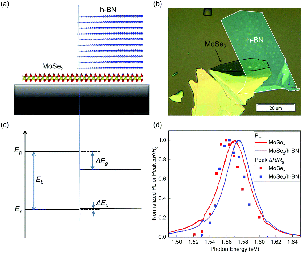 | ||
| Fig. 1 (a) Schematics of the sample structure. (b) Optical microscope image of one of the samples used in this study. (c) Energy diagram of the sample showing the bandgap (Eg) and exciton energy (Ex) of the uncovered (left) and covered regions of the MoSe2 monolayer (right). (d) Normalized photoluminescence (curves) and peak differential reflection signal (symbols) measured from the uncovered (red) and covered (blue) regions of MoSe2. | ||
Due to the screening effect of the h-BN top layer, the electronic structure of the MoSe2 monolayer is expected to be modified.10,27–29Fig. 1(c) shows the transport bandgap (Eg), the optical bandgap (or exciton energy, Ex), and the exciton binding energy (Eb) of the uncovered (left) and covered (right) regions of the MoSe2 monolayer, where Eg = Ex + Eb. Due to the screening effect of h-BN, Eg is reduced by an amount of ΔEg. Previous studies have revealed that the screening effect on the electron–hole interaction also reduces Eb by a similar amount. As a result, the change of Ex, ΔEx = ΔEg−ΔEb, can be very small.10,27–29
2.2 Photoluminescence spectroscopy
In photoluminescence (PL) measurements, a 405 nm continuous-wave laser beam was focused through a microscope objective lens to a size of about 1 μm. The resulting PL emission spectra are shown in Fig. 1(d) for the uncovered (red curve) and covered regions (blue curve) of MoSe2, respectively. Both spectra are normalized for better comparison. In both regions, the PL is dominated by the radiative recombination of the A-excitons in MoSe2.30 The PL peak energy of the covered region is about 12 meV larger than that of the uncovered region. Furthermore, the PL peak of the covered region is higher by a factor of about 2.4 than that from the uncovered region. The small change of the PL energy can be attributed to the near-perfect cancellation of the changes in Eg and Eb by h-BN.10,27–29 It is interesting to note that the sign of ΔEx shows that the change in Eb is slightly larger than that of Eg. We note that the optical measurements performed here can only obtain ΔEx. However, it has been reported that the change of Eg could be on the order of a fraction of 1 eV.10 In addition, the h-BN of 5–10 nm is expected to be thick enough to screen the majority part of the field, producing the nearly maximum effect.2.3 Spatially resolved transient absorption measurements
The spatiotemporally resolved differential reflection measurements were performed with a transient absorption microscope. A Ti-doped sapphire laser produces 100 fs pulses near 790 nm, with a repetition rate of 80 MHz. Part of this output was directly used as the probe pulse. The rest of it was used to pump an optical parametric oscillator to produce a 1400 nm signal output, which is frequency-doubled to 700 nm, serving as the pump pulse. The two beams are combined by a beamsplitter and are send to a microscope objective lens. The reflected probe is sent to a silicon photodiode, the output of which is measured by a lock-in amplifier referenced to a chopper that modulates the pump intensity at about 2 kHz. The spatial scan is achieved by tilting a mirror in the pump arm with a motorized mirror mount. The time scan is done by controlling the length of the pump arm by a linear stage. Differential reflection of the probe is measured, which is defined as ΔR/R0 = (R − R0)/R0. Here, R and R0 are the probe reflection with and without the pump beam, respectively. We confirm that under the experimental conditions used here, the differential reflection is approximately proportional to the injected carrier density.31,32 Hence, its spatial and temporal variations reflect the spatiotemporal dynamics of the photocarriers.3 Results and discussion
We first measured the peak differential reflection on each side of the junction as a function of the probe photon energy. The 1.75 eV pump pulse with a fluence of about 14 μJ cm−2 injects a peak carrier density of about 4.8 × 1011 cm−2, based on an absorption coefficient of 1.37 × 10⁷ m−1 in MoSe2 for this pump energy.33 The normalized peak differential reflection at each probe energy is shown in Fig. 1(d) as the red and blue symbols for the uncovered and covered regions, respectively. In these measurements, the probe delay is close to zero such that the differential reflection signal is the maximum. The spectral shape of the peak differential reflection signal is similar to the PL line shape. In each region, the peak differential reflection spectrum appears to be red-shifted with respect to the PL peak. Similar to the PL results, there is a noticeable blue shift (about 10 meV) of the peak when covered with h-BN.We next time-resolved the photocarrier dynamics by measuring the differential reflection signal as a function of probe delay. The red symbols in Fig. 2 show the signal obtained with the 1.75 eV-pump and 1.57 eV-probe spots overlapped and located in the uncovered region. The same pump fluence of 14 μJ cm−2 was used in this measurement. The inset of Fig. 2 shows the data at early probe delays. The rapid drop of the signal before 1 ps can be attributed to the formation of excitons from the injected electron–hole pairs.34,35 The rest of the decay can be fit by a bi-exponential function with a background, ΔR/R0 = A0 + A1e−t/τ1 + A2e−t/τ2, as shown by the light-gray curve over the red symbols in the main panel. The two decay constants are 16 ± 2 and 114 ± 4 ps, respectively. According to previous studies, the fast time constants could reflect the impact of multi-exciton processes, while the slow time constant can be attributed to the nonradiative recombination lifetime of excitons.32 Moving the laser spots to the h-BN covered region, we studied the photocarrier dynamics in that region (blue symbols in Fig. 2). The peak signal is 2.33 times higher. This factor is close to the ratio of the PL intensities of the two regions, suggesting that the difference is mainly caused by the difference in the pump powers delivered to the MoSe2 layers. The two time constants are 16 ± 2 and 88 ± 4 ps, respectively. The decreased exciton lifetime when covered with h-BN could be attributed to the decreased exciton binding energy from the dielectric screening.
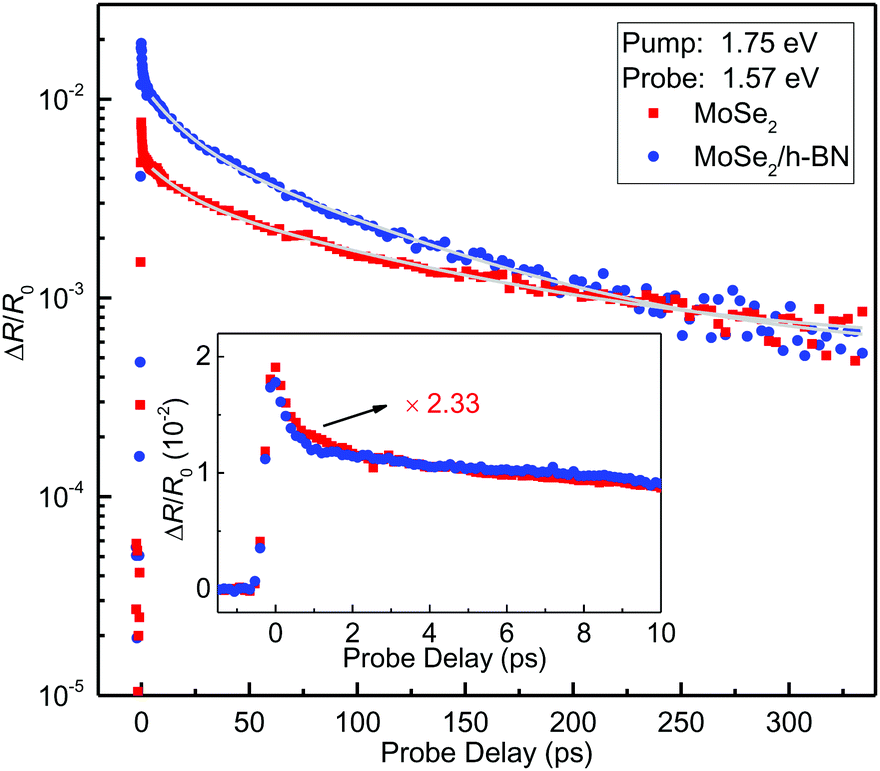 | ||
| Fig. 2 Differential reflection signal of a 1.57 eV probe measured from the uncovered (red squares) and covered (blue circles) regions of the MoSe2 monolayer sample, under the pump of 1.75 eV. The light-gray curves are bi-exponential fits. The inset provides a closer view of the data in early probe delays, with the data from the uncovered region scaled by a factor of 2.33. | ||
We now show the results of spatiotemporally resolved differential reflection measurements to reveal the transfer of excitons across the junction between the two regions. For these measurements, the 1.57 eV probe spot with a full-width at half maximum of about 0.6 μm is centered near the junction. A 1.68 eV pump spot of a similar size was used to inject carriers with a peak density of about 1012 cm−2. The pump spot is scanned across the probe spot along the direction normal to the junction. At each pump position, the differential reflection signal was measured as a function of the probe delay. The results are shown in Fig. 3(a). The vertical black line represents the estimated position of the junction between the covered and uncovered regions. Clearly, the peak of the measured spatial profile shifts towards the direction of the uncovered region over time. This suggests that excitons formed in the covered region of the sample move across the junction into the uncovered region, driven by the energy offset. The corresponding profiles for various probe delays are plotted in Fig. 3(b) as the symbols, from which the peak shift is also clearly visible.
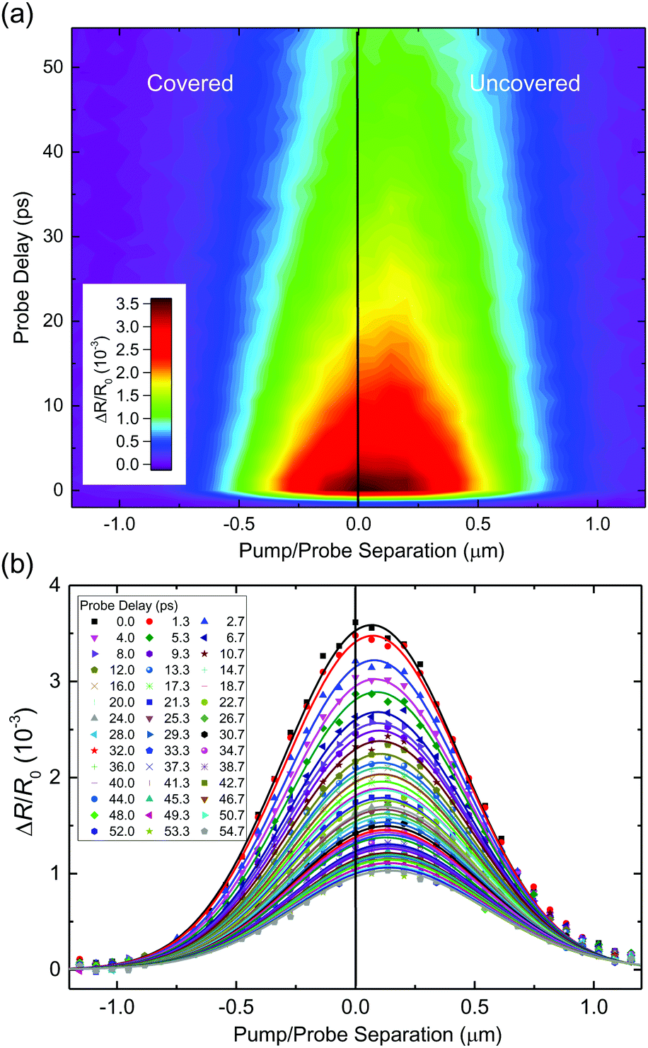 | ||
| Fig. 3 (a) Spatiotemporally resolved differential reflection measurements on a junction between covered and uncovered monolayer MoSe2. (b) Spatial profiles at each probe delay for the data in (a). | ||
Although the shift of the peak position is a clear indication of the exciton transport across the junction, to quantify this process, it is necessary to deconvolute the measured profiles with the finite probe spot, since the shift is much smaller than the spot sizes used in the measurement. For this purpose, we used a rigid-shift model: the exciton spatial profile at zero time was represented by the sum of two half Gaussian functions that are connected at the junction. The heights of the two halves are adjusted to match the excitation density difference of the covered and uncovered regions. For each probe delay, the half-Gaussian function of the covered side was shifted across the junction by a certain displacement. The resulted profile (that is, the sum of the two halves) is convoluted with the profile spot. The result is compared with the data and when needed, the displacement was adjusted to fit the data. Details of this procedure are given in the ESI.† As shown by the curves in Fig. 3(b), this procedure produced profiles that reasonably agree with the data. The peak position extracted by the model is plotted in Fig. 4(a). We note that the shift of the peak position of several tens of nanometers is smaller than the laser spots of 0.6 μm. However, since the shift is determined by the fit of the entire profile, it is not limited by the laser spot. Fig. 4(b) summarizes the displacement of the profile deduced from the model. The exciton profile in the covered region moves with an initial speed of about 10 nm ps−1, which drops to about a quarter of this value in about 30 ps. Due to the simple rigid shift model used, the speed extracted should be viewed as an order-of-magnitude estimate. Understanding the exciton transport at a quantitative level as well as the dependence on the energy offset requires a more sophisticated model, which is beyond the scope of this experimental work.
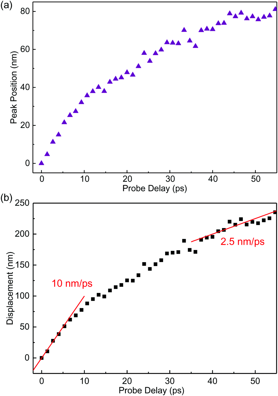 | ||
| Fig. 4 (a) Peak position of the spatial profile from the model shown in Fig. 3(b) as a function of probe delay. (b) The displacement of the profile deduced from the model as a function of the probe delay. | ||
4 Conclusions
In summary, we have demonstrated control of exciton transport through the dielectric screening effect. Photoluminescence and differential reflection measurements showed that covering monolayer MoSe2 with h-BN increases its optical bandgap by about 12 meV. Spatiotemporally resolved differential reflection measurements performed at the junction between the uncovered and h-BN-covered regions revealed that such an offset can drive excitons from the covered to the uncovered regions, with an initial speed on the order of 10 nm ps−1. These results illustrate the feasibility of using van der Waals dielectric engineering to control exciton transport and contribute to understanding the effects of the dielectric environment on the electronic and optical properties of two-dimensional semiconductors.Conflicts of interest
There are no conflicts to declare.Acknowledgements
We are grateful for the financial support of the National Key R&D Program of China (2016YFA0202302), the National Natural Science Foundation of China (61527817, 61875236), the National Science Foundation of USA (DMR-1505852), and the KU Research GO project.References
- A. A. High, E. E. Novitskaya, L. V. Butov, M. Hanson and A. C. Gossard, Science, 2008, 321, 229–231 CrossRef CAS.
- G. Grosso, J. Graves, A. T. Hammack, A. A. High, L. V. Butov, M. Hanson and A. C. Gossard, Nat. Photonics, 2009, 3, 577–580 CrossRef CAS.
- E. Gibney, Nature, 2015, 522, 274–276 CrossRef CAS.
- Q. H. Wang, K. Kalantar-Zadeh, A. Kis, J. N. Coleman and M. S. Strano, Nat. Nanotechnol., 2012, 7, 699–712 CrossRef CAS.
- A. Chernikov, T. C. Berkelbach, H. M. Hill, A. Rigosi, Y. L. Li, O. B. Aslan, D. R. Reichman, M. S. Hybertsen and T. F. Heinz, Phys. Rev. Lett., 2014, 113, 076802 CrossRef.
- K. He, N. Kumar, L. Zhao, Z. Wang, K. F. Mak, H. Zhao and J. Shan, Phys. Rev. Lett., 2014, 113, 026803 CrossRef.
- M. Kulig, J. Zipfel, P. Nagler, S. Blanter, C. Schuller, T. Korn, N. Paradiso, M. M. Glazov and A. Chernikov, Phys. Rev. Lett., 2018, 120, 207401 CrossRef CAS.
- D. Unuchek, A. Ciarrocchi, A. Avsar, K. Watanabe, T. Taniguchi and A. Kis, Nature, 2018, 560, 340 CrossRef CAS.
- J. He, N. Kumar, M. Z. Bellus, H. Y. Chiu, D. He, Y. Wang and H. Zhao, Nat. Commun., 2014, 5, 5622 CrossRef CAS.
- A. Raja, A. Chaves, J. Yu, G. Arefe, H. M. Hill, A. F. Rigosi, T. C. Berkelbach, P. Nagler, C. Schuller, T. Korn, C. Nuckolls, J. Hone, L. E. Brus, T. F. Heinz, D. R. Reichman and A. Chernikov, Nat. Commun., 2017, 8, 15251 CrossRef.
- S. M. Cui, H. H. Pu, S. A. Wells, Z. H. Wen, S. Mao, J. B. Chang, M. C. Hersam and J. H. Chen, Nat. Commun., 2015, 6, 8632 CrossRef CAS.
- Z. B. Song, T. Schultz, Z. J. Ding, B. Lei, C. Han, P. Amsalem, T. T. Lin, D. Z. Chi, S. L. Wong, Y. J. Zheng, M. Y. Li, L. J. Li, W. Chen, N. Koch, Y. L. Huang and A. T. S. Wee, ACS Nano, 2017, 11, 9128–9135 CrossRef CAS.
- J. H. Kim, J. Lee, J. H. Kim, C. C. Hwang, C. Lee and J. Y. Park, Appl. Phys. Lett., 2015, 106, 251606 CrossRef.
- Y. Li, C. Y. Xu and L. Zhen, Appl. Phys. Lett., 2013, 102, 143110 CrossRef.
- P. Bolshakov, P. Zhao, A. Azcatl, P. K. Hurley, R. M. Wallace and C. D. Young, Appl. Phys. Lett., 2017, 111, 032110 CrossRef.
- J. S. Ross, P. Klement, A. M. Jones, N. J. Ghimire, J. Yan, D. G. Mandrus, T. Taniguchi, K. Watanabe, K. Kitamura, W. Yao, D. H. Cobden and X. Xu, Nat. Nanotechnol., 2014, 9, 268–274 CrossRef CAS.
- A. Pospischil, M. M. Furchi and T. Mueller, Nat. Nanotechnol., 2014, 9, 257–261 CrossRef CAS.
- B. W. H. Baugher, H. O. H. Churchill, Y. Yang and P. Jarillo-Herrero, Nat. Nanotechnol., 2014, 9, 262–267 CrossRef CAS.
- Y. Katagiri, T. Nakamura, C. Ohata, S. Katsumoto and J. Haruyama, Appl. Phys. Lett., 2017, 110, 143109 CrossRef.
- M. S. Choi, D. Qu, D. Lee, X. Liu, K. Watanabe, T. Taniguchi and W. J. Yoo, ACS Nano, 2014, 8, 9332–9340 CrossRef CAS.
- L. Meng, Y. H. Zhang, S. Hu, X. F. Wang, C. S. Liu, Y. D. Guo, X. R. Wang and X. H. Yan, Appl. Phys. Lett., 2016, 108, 263104 CrossRef.
- F. Ceballos, P. Zereshki and H. Zhao, Phys. Rev. Mater., 2017, 1, 044001 CrossRef.
- M. Z. Bellus, M. Li, S. Lane, F. Ceballos, Q. Cui, X. C. Zeng and H. Zhao, Nanoscale Horiz., 2016, 2, 31–36 RSC.
- S. Tongay, J. Zhou, C. Ataca, K. Lo, T. S. Matthews, J. B. Li, J. C. Grossman and J. Q. Wu, Nano Lett., 2012, 12, 5576–5580 CrossRef CAS.
- P. Tonndorf, R. Schmidt, P. Bottger, X. Zhang, J. Borner, A. Liebig, M. Albrecht, C. Kloc, O. Gordan, D. R. T. Zahn, S. M. de Vasconcellos and R. Bratschitsch, Opt. Express, 2013, 21, 4908 CrossRef CAS.
- M. Z. Bellus, Z. Yang, P. Zereshki, J. Hao, S. P. Lau and H. Zhao, Nanoscale Horiz., 2018, 4, 236 RSC.
- G. Gupta, S. Kallatt and K. Majumdar, Phys. Rev. B: Condens. Matter Mater. Phys., 2017, 96, 081403 CrossRef.
- K. T. Winther and K. S. Thygesen, 2D Mater., 2017, 4, 025059 CrossRef.
- Y. S. Cho and T. C. Berkelbach, Phys. Rev. B: Condens. Matter Mater. Phys., 2018, 97, 041409 CrossRef CAS.
- Y. Li, A. Chernikov, X. Zhang, A. Rigosi, H. M. Hill, A. M. van der Zande, D. A. Chenet, E.-M. Shih, J. Hone and T. F. Heinz, Phys. Rev. B: Condens. Matter Mater. Phys., 2014, 90, 205422 CrossRef.
- N. Kumar, Q. Cui, F. Ceballos, D. He, Y. Wang and H. Zhao, Phys. Rev. B: Condens. Matter Mater. Phys., 2014, 89, 125427 CrossRef.
- F. Ceballos and H. Zhao, Adv. Funct. Mater., 2017, 27, 1604509 CrossRef.
- H.-L. Liu, C.-C. Shen, S.-H. Su, C.-L. Hsu, M.-Y. Li and L.-J. Li, Appl. Phys. Lett., 2014, 105, 201905 CrossRef.
- F. Ceballos, Q. Cui, M. Z. Bellus and H. Zhao, Nanoscale, 2016, 8, 11681–11688 RSC.
- P. Steinleitner, P. Merkl, P. Nagler, J. Mornhinweg, C. Schuller, T. Korn, A. Chernikov and R. Huber, Nano Lett., 2017, 17, 1455–1460 CrossRef CAS.
Footnote |
| † Electronic supplementary information (ESI) available: Raman spectrum of monolayer MoSe2 and discussion of the rigid-shift model. See DOI: 10.1039/c9nh00462a |
| This journal is © The Royal Society of Chemistry 2020 |